DOI:
10.1039/C6RA07037J
(Communication)
RSC Adv., 2016,
6, 48319-48323
Enhancing performance of ZnO/NiO UV photodetector by piezo-phototronic effect†
Received
17th March 2016
, Accepted 9th May 2016
First published on 11th May 2016
Abstract
In this work, a UV photodetector based on a ZnO/NiO core/shell nanorods array is fabricated by hydrothermal growth processes and thermal oxidation. Compressive strain is applied to enhance the Ilight and sensitivity of the UV photodetectors. Under a 1 N compressive strain at −3.5 V, the enhancement in Ilight and sensitivity of the UV photodetector is about 74% and 78.7%, respectively. The possible working principle is that the negative piezo-polarization at the ZnO/NiO interface shifts the depletion region to the ZnO side leading to an increase of the photon-absorption volume. This work may provide a potential approach to enhance the performance of the ZnO/NiO UV photodetector.
Introduction
Nowadays, ultraviolet (UV) photodetectors (PDs) of different materials and mechanisms are widely used in various applications such as solar-blind detectors, environmental monitoring, and chemical analysis.1–3 In order to improve the performance, a lot of semiconductor materials have been synthesized and used to fabricate UV photodetectors such as SiC,4 GaN,5,6 and AlGaN.7 ZnO is a potential absorber material with low-cost processing and simple synthesis, making it an alternative to GaN or SiC.8 It has thus attracted significant research interest.9–16 The heterojunction photodetectors based on ZnO are becoming some of the most suitable building blocks for future optoelectronic applications due to the low dark current and fast responding speed. So far, various materials have been used to enhance the performance of ZnO photodetectors such as PEDOT![[thin space (1/6-em)]](https://www.rsc.org/images/entities/char_2009.gif) :PSS,17 Ag,18 NiO,19,20 Al2O3,21 ZnS.22,23 Among these materials, NiO has been under investigation for the fabrication of p-NiO/n-ZnO heterojunction based UV photodetectors due to its wide direct band gap (3.7 eV) and it is intrinsically p-type semiconductor. Particularly, alternative and inexpensive fabrication techniques are usually needed to realize large scale, mass production and low cost UV photodetectors with high performance. In addition, the unique coupled piezoelectric and semiconducting properties of ZnO have been forming a new field of piezotronics, which has been demonstrated as an effective approach to enhance the performance of solar cells,24 light emitting diodes,25 pressure sensors26 and photodetectors22,27–30 by modulating the charge carrier transport, separation, or recombination across the local surface/interface through strain-induced piezoelectric polarization charges.31–34 However, compared with the relatively simple cases in Schottky junctions, piezo-phototronics effect in p–n junction induces much more complicated change in the depletion region and the band gap. Thus, the different morphologies of the oxides at the interface will obviously influence device performance. For example, in the previous work,26 the p-NiO/n-ZnO heterojunction is used to fabricate the pressure sensors. In the pressure sensor, the NiO layer is about 10 nm, and the electrons pass through the potential barrier at the ZnO/NiO interface mainly by tunneling effect. The device is more sensitive to pressure than UV light. The UV light is used to weaken the influence of bulk resistance and create more electrons tunnelling through the barrier layer.
:PSS,17 Ag,18 NiO,19,20 Al2O3,21 ZnS.22,23 Among these materials, NiO has been under investigation for the fabrication of p-NiO/n-ZnO heterojunction based UV photodetectors due to its wide direct band gap (3.7 eV) and it is intrinsically p-type semiconductor. Particularly, alternative and inexpensive fabrication techniques are usually needed to realize large scale, mass production and low cost UV photodetectors with high performance. In addition, the unique coupled piezoelectric and semiconducting properties of ZnO have been forming a new field of piezotronics, which has been demonstrated as an effective approach to enhance the performance of solar cells,24 light emitting diodes,25 pressure sensors26 and photodetectors22,27–30 by modulating the charge carrier transport, separation, or recombination across the local surface/interface through strain-induced piezoelectric polarization charges.31–34 However, compared with the relatively simple cases in Schottky junctions, piezo-phototronics effect in p–n junction induces much more complicated change in the depletion region and the band gap. Thus, the different morphologies of the oxides at the interface will obviously influence device performance. For example, in the previous work,26 the p-NiO/n-ZnO heterojunction is used to fabricate the pressure sensors. In the pressure sensor, the NiO layer is about 10 nm, and the electrons pass through the potential barrier at the ZnO/NiO interface mainly by tunneling effect. The device is more sensitive to pressure than UV light. The UV light is used to weaken the influence of bulk resistance and create more electrons tunnelling through the barrier layer.
In contrast, in this work, the device as a UV photodetector is more sensitive to the UV light than pressure due to the thickness of the NiO layer and the bulk resistance of the sample. The influence of piezo-charges is mainly changing the depletion region, leading to increase the photon-absorption volume. For the UV photodetector, there are two back-to-back and opposite ZnO/NiO barriers, which is helpful for the improvement of sensitivity due to the lower dark current compared with the device with a single ZnO/NiO barrier.35 Under a 1 N loading, the sensitivity of the photodetector can be further improved about 78.7% by piezo-phototronic effect. These results indicate that the piezo-phototronic effect can effectively enhance the performance of the ZnO/NiO UV photodetector.
Experimental
The design of the photodetector based on the ZnO/NiO core/shell nanorods array is shown in Fig. 1. ZnO nanorods were grown on c-plane sapphire substrates using the hydrothermal method. The c-plane sapphire substrate is cut as 0.5 cm × 1.5 cm pieces. Before the growth of ZnO NRs, the substrates were cleaned ultrasonically in acetone, ethanol and deionized water. Then, a 20 nm thick ZnO seed layer was deposited on the substrates by room temperature radio frequency (RF) magnetron sputtering. The background pressure of the vacuum chamber was 1 × 10⁻⁴ Pa and argon was used as the sputtering gas with a pressure of 3.5 Pa. After that the ZnO NRs were grown from the ZnO seeds by a simple and low-cost hydrothermal process.36,37 The aqueous solution used here was composed of a 30 mmol L−1 1:1 ratio of zinc acetate dehydrate and hexamethylenetetramine (HMTA). The aqueous solution was fully and evenly stirred and then transferred into a Teflon reaction kettle in which the sample was suspended vertically. The reaction was carried out at 95 °C for 4 h. After the reaction, the samples were taken out of the solution, rinsed with deionized water and then air-dried. The next step was depositing Ni on ZnO nanorods array by mask thermal evaporation in a vacuum chamber with a pressure of 2 × 10⁻⁴ Pa. The Ni was oxidized in a furnace at 900 °C for 1 h under an air atmosphere. The NiO/ZnO core/shell heterojunctions are formed at the two ends of the substrate about 0.5 cm × 0.5 cm, as shown in Fig. 1(c). Then, two pieces of ITO glass covered on the as-prepared sample as electrode. Testing wires were connected to ITO glasses by silver paste. A piece of glass covered on the sample for applying compressive strain. Finally, the whole device was fully packaged with a flexible polymer film.
 |
| | Fig. 1 (a)–(d) Schematic illustration of the ZnO/NiO core/shell nanorods photodetector fabrication process. | |
Characterization
The structural and morphological properties of the photodetector were examined by X-ray diffraction (XRD), field emission scanning electron microscope (FESEM). The photoelectric properties of the photodetectors were characterized using a semiconductor characterization system (Keithley 4200) under UV (365 nm) illumination (17 mW).
Results and discussion
Fig. 2(a) and (b) show the SEM images of the ZnO and ZnO/NiO core/shell nanorods, respectively, which show the ZnO nanorods are hexagonal prismatic in shape with diameter of 400–500 nm and length of ∼1.5 μm. The formation of NiO shell layer on the ZnO nanorods is evidenced by Fig. 2(b). After coating, the diameter of the ZnO/NiO core/shell nanorods is larger than ZnO nanorods because of the NiO coating. Fig. 2(c) shows the EDS spectrum of the ZnO/NiO core/shell nanorods in which Zn, O and Ni are detected. Fig. 3 shows the XRD patterns of the ZnO and ZnO/NiO core/shell nanorods grown on sapphires. Diffraction peaks characteristic of ZnO, such as ZnO (002), (101), are still observed after NiO coating. However, the (101) peak is almost negligible compared with the (002) peak. And the NiO diffraction peak almost can not be found due to the high intensity of the ZnO (002) peak, which indicates that the ZnO nanorods are highly oriented and exhibit good crystallinity. To observe the NiO diffraction peak, the enlarged view of the XRD patterns of the ZnO and ZnO/NiO core/shell nanorods is shown in Fig. 3(b). The typical diffraction peaks (111) and (200) of NiO are clearly observed, which agree with those of standard NiO of cubic structure. These results confirm that ZnO/NiO core/shell nanorods are synthesized by hydrothermal growth processes and thermal oxidation.
 |
| | Fig. 2 (a) and (b) SEM images of ZnO and ZnO/NiO core/shell nanorods. (c) EDX spectrum from (b). | |
 |
| | Fig. 3 (a) XRD patterns of ZnO and ZnO/NiO core/shell nanorods. (b) The enlarged view of the XRD patterns of the ZnO and ZnO/NiO core/shell nanorods. | |
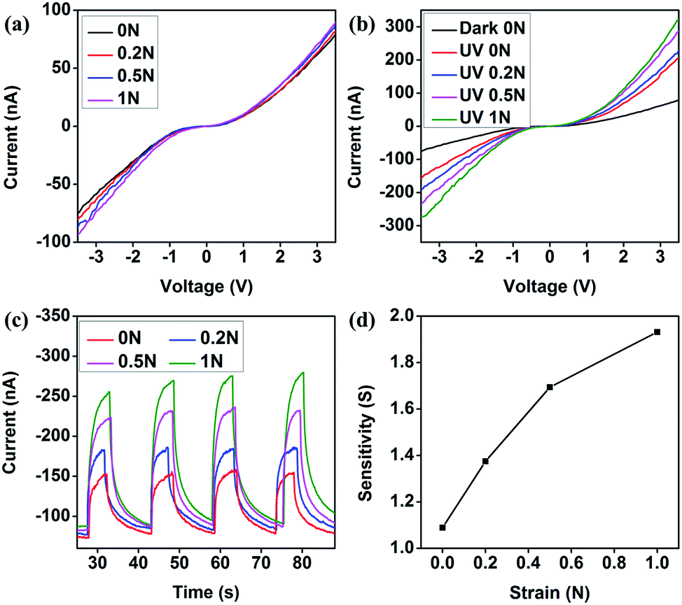
As shown in Fig. 5(a), there is a ZnO/NiO junction at each of the two electrodes. The I–V characteristics of the device under different external strain conditions and without any illumination are first measured and plotted in Fig. 4(a). The symmetric rectifying I–V curves indicate that there were two back-to-back PN junctions in the device. It can be seen that the piezoelectric effect on the I–V curve in the dark is not obvious due to the bulk resistance of the sample.26,35 In the dark, the surface of the ZnO NRs is depleted by absorbed oxygen molecules which increase the bulk resistance of ZnO NRs. The current is controlled by both the bulk resistance of the sample and the two back-to-back PN junctions at ZnO/NiO interface. Under UV illumination, electron–hole pairs are photo-generated and holes are readily trapped at the surface, leaving behind unpaired electrons, which increase the conductivity of the ZnO nanorods and weaken the influence of bulk resistance. Therefore, the two back-to-back PN junctions play a crucial role in determining the electrical transport property. Fig. 4(b) shows the I–V curves of the device under different strains with UV light. At −3.5 V bias condition, the absolute value of the photocurrent (Ilight) rises, from 157 nA to 191 nA, to 235 nA, to 273 nA, about 74% with the strain increasing from 0 N, to 0.2 N, to 0.5 N, to 1 N. Fig. 4(c) shows the response behaviors of the devices with and without strain at bias of −3.5 V. The current can fully recover and has no drift even after repeated cycles, which demonstrates that this photodetector has good stability and repeatability. The performance of the ZnO-only photodetector is also investigated and the result is shown in Fig. S1 (ESI†). It can be found that the decay time of 10 s for the ZnO/NiO device is nearly 2 times shorter than that of the ZnO device (20 s). The sensitivity (S) defined as (Ilight − Idark)/Idark is shown in Fig. 4(d). With the strain increasing from 0N, to 0.2 N, to 0.5 N, to 1 N, the sensitivity (S) of −3.5 V bias rises step by step, from 1.08 to 1.37, to 1.69, to 1.93, nearly 78.7%, indicating the piezo-phototronic effect can enhance performance of the ZnO/NiO UV photodetector.
 |
| | Fig. 4 (a) The I–V characteristic curves of the photodetector under different strains without UV light. (b) The I–V characteristic curves of the photodetector under different strains with UV light. (c) Time dependence of the photocurrent with/without strains. (d) The plots of sensitivity (S) at a fixed bias of −3.5 V as a function of compressive strain. | |
 |
| | Fig. 5 (a) Schematic illustration of the photodetector under compressive strain. (b) Schematic energy band structure of ZnO/NiO heterojunction with and without compressive strain, shown in red and black curves, respectively. | |
The performance enhancing of the UV photodetector by the piezo-phototronic effect can be understood from the shift of depletion region.31,34 For the NiO/ZnO/NiO (PNP) structure, there are two back-to-back and opposite PN junctions, as shown in Fig. 5(a). Thus, when a fixed bias voltage V is applied across the photodetector, the voltage drop occurs mainly at the reversely biased PN junction.38,39 As shown in Fig. 5(b), under compressive strain, the negative piezoelectric charges distribute at the ZnO/NiO interface. When piezo-charges are present, the depletion width can be described as:39
| | |
NAWDp = NDWDn + ρpiezoWpiezo
| (1) |
NA is the p-type doping density in the p-type region,
ND is the n-type doping density in the n-type region,
WDp is the depletion width in the p-type region,
WDn is the depletion width in the n-type region,
Wpiezo is the width of piezo-charges distributing at the interface of p–n junction, and
ρpiezo is the density of polarization charges.
According to eqn (1), under compressive strain, the depletion width on the p-NiO side is reduced and the depletion width on the n-ZnO side is increased by negative piezo-polarization charges present at local interface of the ZnO/NiO.34,39 The depletion region expands and shifts toward the n-ZnO side, and shrinks on the p-NiO side. Under UV light, this expansion of the depletion region on the ZnO side will effectively increase the photon-absorption volume and thus lead to an enhancement in Ilight. This is the working principle of piezo-phototronic effect enhanced UV photodetector based on ZnO/NiO core/shell nanorods array.
Conclusion
In summary, we have successfully fabricated the UV photodetector based on ZnO/NiO core/shell nanorods array by hydrothermal growth processes and thermal oxidation. Due to the coupled semiconducting and piezoelectric properties of ZnO, the performance of the UV photodetector could be enhanced by introducing strain. Under a 1 N compressive strain at −3.5 V, the enhancement in Ilight and sensitivity of the UV photodetector is about 74% and 78.7%, respectively. The working principle is that the negative piezo-polarization charges at the ZnO/NiO interface shifts the depletion region to ZnO side, leading to increase the photon-absorption volume. This work may provide a potential approach to enhance the performances of ZnO UV photodetectors.
Acknowledgements
This work was supported by the NSFC (Project No. 61504018), the Fundamental Research Funds for the Central Universities (DUT14LK35), Foundation of Key laboratory for Micro/Nano Technology and System of Liaoning and Province (20140405), the Fundamental Research Funds for the Central Universities (DUT15LAB15), the Doctoral Scientific Research Foundation of Liaoning Province (Project No. 201501193), and General Project of Scientific Research of the Education Department of Liaoning Province (L2015040).
References
- W.-D. Li and S. Y. Chou, Opt. Express, 2010, 18, 931–937 CrossRef CAS PubMed.
- M. Razeghi and A. Rogalski, J. Appl. Phys., 1996, 79, 7433–7473 CrossRef CAS.
- E. Monroy, F. Omnès and F. Calle, Semicond. Sci. Technol., 2003, 18, R33 CrossRef CAS.
- N. Naderi and M. R. Hashim, J. Alloys Compd., 2013, 552, 356–362 CrossRef CAS.
- N. Vanhove, J. John, A. Lorenz, K. Cheng, G. Borghs and J. E. M. Haverkort, Appl. Surf. Sci., 2006, 253, 2930–2932 CrossRef CAS.
- W. Y. Weng, T. J. Hsueh, S. J. Chang, S. B. Wang, H. T. Hsueh and G. J. Huang, IEEE J. Sel. Top. Quantum Electron., 2011, 17, 996–1001 CrossRef CAS.
- I.-S. Seo, I.-H. Lee, Y.-J. Park and C.-R. Lee, J. Cryst. Growth, 2003, 252, 51–57 CrossRef CAS.
- D.-C. Perng, H.-P. Lin and M.-H. Hong, Appl. Phys. Lett., 2015, 107, 241113 CrossRef.
- B. Yin, Y. Qiu, H. Zhang, J. Ji and L. Hu, CrystEngComm, 2014, 16, 6831–6835 RSC.
- B. Liu, J. Xu, S. Ran, Z. Wang, D. Chen and G. Shen, CrystEngComm, 2012, 14, 4582–4588 RSC.
- W. Cheng, L. Tang, J. Xiang, R. Ji and J. Zhao, RSC Adv., 2016, 6, 12076–12080 RSC.
- A. A. Chaaya, M. Bechelany, S. Balme and P. Miele, J. Mater. Chem. A, 2014, 2, 20650–20658 CAS.
- Z. Zhang, Q. Liao, Y. Yu, X. Wang and Y. Zhang, Nano Energy, 2014, 9, 237–244 CrossRef CAS.
- X.-W. Fu, Z.-M. Liao, J. Xu, X.-S. Wu, W. Guo and D.-P. Yu, Nanoscale, 2013, 5, 916–920 RSC.
- J. Dai, C. Xu, X. Xu, J. Guo, J. Li, G. Zhu and Y. Lin, ACS Appl. Mater. Interfaces, 2013, 5, 9344–9348 CAS.
- M. Ding, D. X. Zhao, B. Yao, Z. P. Li and X. J. Xu, RSC Adv., 2015, 5, 908–912 RSC.
- P. Lin, X. Yan, Z. Zhang, Y. Shen, Y. Zhao, Z. Bai and Y. Zhang, ACS Appl. Mater. Interfaces, 2013, 5, 3671–3676 CAS.
- X. Zhao, F. Wang, L. Shi, Y. Wang, H. Zhao and D. Zhao, RSC Adv., 2016, 6, 4634–4639 RSC.
- J. R. n. D. n. Retamal, C.-Y. Chen, D.-H. Lien, M. R. Huang, C.-A. Lin, C.-P. Liu and J.-H. He, ACS Photonics, 2014, 1, 354–359 CrossRef CAS.
- D. Y. Kim, J. Ryu, J. Manders, J. Lee and F. So, ACS Appl. Mater. Interfaces, 2014, 6, 1370–1374 CAS.
- R. Aga Jr, D. Jowhar, A. Ueda, Z. Pan, W. Collins, R. Mu, K. Singer and J. Shen, Appl. Phys. Lett., 2007, 91, 232108 CrossRef.
- S. C. Rai, K. Wang, Y. Ding, J. K. Marmon, M. Bhatt, Y. Zhang, W. Zhou and Z. L. Wang, ACS Nano, 2015, 9, 6419–6427 CrossRef CAS PubMed.
- X. Fang, Z. Wei, R. Chen, J. Tang, H. Zhao, L. Zhang, D. Zhao, D. Fang, J. Li and F. Fang, ACS Appl. Mater. Interfaces, 2015, 7, 10331–10336 CAS.
- X. N. Wen, W. Z. Wu and Z. L. Wang, Nano Energy, 2013, 2, 1093–1100 CrossRef CAS.
- Q. Yang, Y. Liu, C. Pan, J. Chen, X. Wen and Z. L. Wang, Nano Lett., 2013, 13, 607–613 CrossRef CAS PubMed.
- B. Yin, H. Zhang, Y. Qiu, Y. Chang, J. Lei, D. Yang, Y. Luo, Y. Zhao and L. Hu, Nano Energy, 2016, 21, 106–114 CrossRef CAS.
- X. W. Fu, Z. M. Liao, J. Xu, X. S. Wu, W. L. Guo and D. P. Yu, Nanoscale, 2013, 5, 916–920 RSC.
- P. Gao, Z. Z. Wang, K. H. Liu, Z. Xu, W. L. Wang, X. D. Bai and E. G. Wang, J. Mater. Chem., 2009, 19, 1002–1005 RSC.
- F. Zhang, S. Niu, W. Guo, G. Zhu, Y. Liu, X. Zhang and Z. L. Wang, ACS Nano, 2013, 7, 4537–4544 CrossRef CAS PubMed.
- Y.-Y. Chen, C.-H. Wang, G.-S. Chen, Y.-C. Li and C.-P. Liu, Nano Energy, 2015, 11, 533–539 CrossRef CAS.
- Z. N. Wang, R. M. Yu, X. N. Wen, Y. Liu, C. F. Pan, W. Z. Wu and Z. L. Wang, ACS Nano, 2014, 8, 12866–12873 CrossRef CAS PubMed.
- Y. F. Hu, Y. L. Chang, P. Fei, R. L. Snyder and Z. L. Wang, ACS Nano, 2010, 4, 1234–1240 CrossRef CAS PubMed.
- Y. Zhang, Y. Liu and Z. L. Wang, Adv. Mater., 2011, 23, 3004–3013 CrossRef CAS PubMed.
- Y. Liu, Y. Zhang, Q. Yang, S. Niu and Z. L. Wang, Nano Energy, 2015, 14, 257–275 CrossRef CAS.
- Q. Yang, X. Guo, W. H. Wang, Y. Zhang, S. Xu, D. H. Lien and Z. L. Wang, ACS Nano, 2010, 4, 6285–6291 CrossRef CAS PubMed.
- Z. X. Wang, X. Y. Zhan, Y. J. Wang, S. Muhammad, Y. Huang and J. He, Nanoscale, 2012, 4, 2678–2684 RSC.
- Q. W. Li, J. M. Bian, J. C. Sun, J. W. Wang, Y. M. Luo, K. T. Sun and D. Q. Yu, Appl. Surf. Sci., 2010, 256, 1698–1702 CrossRef CAS.
- Q. Liao, M. Mohr, X. Zhang, Z. Zhang, Y. Zhang and H.-J. Fecht, Nanoscale, 2013, 5, 12350–12355 RSC.
- Z. Wang, R. Yu, X. Wen, Y. Liu, C. Pan, W. Wu and Z. L. Wang, ACS Nano, 2014, 8, 12866–12873 CrossRef CAS PubMed.
Footnote |
| † Electronic supplementary information (ESI) available. See DOI: 10.1039/c6ra07037j |
|
| This journal is © The Royal Society of Chemistry 2016 |
Click here to see how this site uses Cookies. View our privacy policy here.