
Random nanocrack, assisted metal nanowire-bundled network fabrication for a highly flexible and transparent conductor†
Young D. Suh‡
a,
Sukjoon Hong‡a,
Jinhwan Leea,
Habeom Leea,
Seongmin Junga,
Jinhyeong Kwona,
Hyunjin Moona,
Phillip Wona,
Jaeho Shina,
Junyeob Yeo*b and
Seung Hwan Ko*a
aApplied Nano and Thermal Science Lab, Department of Mechanical Engineering, Seoul National University, 1 Gwanak-ro, Gwanak-gu, Seoul 151-742, Korea. E-mail: maxko@snu.ac.kr
bDepartment of Physics, Kyungpook National University, 80 Daehak-ro, Pook-gu, Daegu 41566, Korea. E-mail: junyeob@knu.ac.kr
First published on 3rd June 2016
Abstract
The most viable flexible and transparent conductor alternative to indium tin oxide (ITO) is metal mesh on plastic including metal micro-lines at regular spacing and metal nanowire percolation networks. Applications in flexible and transparent devices have been hampered by either moiré pattern problems caused by regular patterning or low mechanical robustness of the nanowire network. In this study, we demonstrate a novel class of flexible transparent conductor based on metal nanowire micro-bundled networks at random patterns. Original random patterns are prepared from controlled random cracking of high-stress silicon nitride on the silicon substrate, and employed as repetitively usable master molds with independently controllable pattern density and linewidth. Silver nanowires are subsequently placed in the random crack channels through a facile solution process and transferred to the polymer substrate with UV curable epoxy resin. The resultant flexible and transparent conductor, spanning over wafer scale at high reproducibility, not only exhibits enhanced mechanical robustness upon repeated bending or scratching, which often occurs when used as touch-screen panel, but also is free from the moiré pattern problem due to the random nature of nanowire bundle patterns. Further application of the resultant flexible transparent conductor as a touch-screen panel confirms easy large-scale fabrication of this robust and flexible transparent conductor.
1. Introduction
Recently interest in electrically conductive and optically transparent materials has increased in optoelectronics for applications in solar cells1 and touch-screen displays2 as well as thermo-electronical devices.3,4 Indium tin oxide (ITO) and fluorine tin oxide (FTO) have been abundantly used in the aforementioned fields; however, scarcity of materials and difficulties in the film deposition process5–7 have led to development of alternatives such as metal networks.8,9 Compared to doped metal oxide films, ductility of the metallic networks is advantageous in terms of mechanical stability against deformation such as bending and stretching.10,11Among various metal networks, nanowire percolation networks have been studied widely as a substitute for doped metal oxide film due to its good electrical conductivity, environmentally friendly fabrication process that does not necessitate a high temperature or vacuum environment, and compatibility with a solution process that enables a large-area or roll-to-roll process. Nevertheless, there are still problems with industry-level use of the nanowires such as imperfect uniformity of nanowire networks when dispersed on a substrate and weak adhesion between the nanowires themselves or the nanowires and substrate. Recently, several studies have reported that this weak adhesion issue can be significantly improved while maintaining high electrical and optical properties through embedding nanowire percolation networks within transparent polymer substrate using high aspect ratio nanowires.12
As an alternative to the metal nanowire percolation networks, fracture assisted metallic network fabrication processes have been reported.13–15 In such processes, a random network made by fractures of gel film, photoresist film or dried colloidal layer deposited on a flexible substrate is used as a template for subsequent metal deposition by sputtering or evaporation. The metal networks fabricated in this manner, however, can be used only a single time and require a metal deposition process via a vacuum environment such as a sputtering or evaporation process that increases the overall fabrication cost and time. In addition, due to its single-use nature, the generated crack pattern in the process varies every time, and thus electrical and optical properties of the resultant network may exhibit poor reproducibility. Nevertheless, both metal nanowire percolation networks and crack-assisted metal networks show high optical transmission and electrical conductivity simultaneously yet no optical moiré pattern problems were observed due to randomness of the metal patterns.
In an attempt to develop a new approach that reduces fabrication costs by employing short nanowires, which is beneficial for mass production since synthesis time can be significantly reduced and still take advantage of randomness of the metal network patterns that minimize the moiré effect problem, we utilized random-cracked glassy film deposited on a silicon substrate. As reported in several studies,16–18 high-stress silicon nitride on the silicon substrate leads to nanoscale random cracks in the film. This new approach enables fabrication of transparent conductors for metal nanowire networks with a few micron-scale linewidths on a transparent and flexible substrate and repeatable use of the template, making it suitable for mass production. Via controlled nano-crack generation and subsequent wet-etch post process, we demonstrate fabrication of silver nanowire (Ag NW) network patterns with various linewidths and pattern densities that are directly related to optical transmittance and electrical conductivity. In addition, via a simple touch-screen panel demonstration, we prove that the fabricated metal nanowire network patterns can be directly applied to device fabrication.
2. Experimental section
2.1 Controlled random crack fabrication
Silicon substrates with (100) crystallographic orientation are cleaned via standard MEMS protocol: piranha cleaning followed by native oxide removal by diluted HF solution (10![[thin space (1/6-em)]](https://www.rsc.org/images/entities/char_2009.gif) :1, H2O:HF). Stoichiometric silicon nitride (Si3N4) is deposited by low-pressure chemical vapor deposition (LPCVD) at the temperature and pressure of 800 °C and 200 mTorr, respectively. To induce high stress in the film, dichlorosilane (H2SiCl2) and ammonia (NH3) at 30 cm3 (STP) min−1 and 100 cm3 (STP) min−1 were used. A random network of nano-cracks has 100–150 nm width. Subsequently, the width of nano-cracks can be widened by selective wet etching with HNA solution ranging from 1:9:10 to 2:8:10 ratio mixture to etch the (100) Si substrate. Once the target width of the micro-crack patterns is reached, Si3N4 film is removed by dipping in high-concentration HF (49%) for approximately 2–3 h. The etching rate of Si3N4 by HF (49%) is approximately 500 nm h−1.
:1, H2O:HF). Stoichiometric silicon nitride (Si3N4) is deposited by low-pressure chemical vapor deposition (LPCVD) at the temperature and pressure of 800 °C and 200 mTorr, respectively. To induce high stress in the film, dichlorosilane (H2SiCl2) and ammonia (NH3) at 30 cm3 (STP) min−1 and 100 cm3 (STP) min−1 were used. A random network of nano-cracks has 100–150 nm width. Subsequently, the width of nano-cracks can be widened by selective wet etching with HNA solution ranging from 1:9:10 to 2:8:10 ratio mixture to etch the (100) Si substrate. Once the target width of the micro-crack patterns is reached, Si3N4 film is removed by dipping in high-concentration HF (49%) for approximately 2–3 h. The etching rate of Si3N4 by HF (49%) is approximately 500 nm h−1.
2.2 Filling Ag nanowires in random cracks
Two types of nanowires were prepared by following a previously reported synthesis process19 and by modified polyol method. Approximately 1 mL of 5–10 μm long with 40 nm diameter Ag NW dispersed solution is drop casted on the random crack template. The doctor blading method is used to fill the random crack patterns with the Ag NW ink. As the ink dries, the bundled Ag NWs form as a thin layer within the random crack channels. For complete removal of Ag NW residue, an additional blading process is conducted to scrape residue from the mold's top surface.2.3 Bundled Ag NW network transfer
UV curable epoxy resin (CCTECH, SEA-1) is spun on or bar-coated on the random crack template filled with Ag NW bundles. A 130 μm thick PET film covering an entire wafer size is laid over the template and cured under a multi-wavelength light source (400 W, 350–750 nm) for 1 min. Then the PET film with bundled Ag NW network is detached from the random crack template.3. Results and discussion
Fig. 1a shows the schematic fabrication process for the random crack-assisted, highly flexible and transparent, bundled Ag nanowire networks (BANN) electrode. First, the high-stress thin silicon nitride (Si3N4) film deposited on a silicon substrate induces substantial residual stress in the Si3N4/Si system; in turn severe random cracking occurs over the entire Si3N4 film. The cracks having nanoscale width (100–150 nm) begin to occur as the Si3N4 film thickness passes the crack initiation threshold (approximately 800 nm).16 As the silicon nitride film thickness is increased up to 2 μm, the stored elastic energy in the system is increased greatly, resulting in a dense network of nano-cracks. Because of the elastic mismatch between the Si substrate and Si3N4 (Si substrate is relatively more compliant than the Si3N4 film), significant crack penetration into the substrate is accompanied20 by formation of nano-cracks as found in our previous study.21 However, in contrast to our previous controlled cracking study, we tried to intentionally generate random crack patterns to create a master mold for replicating a highly transparent conductor with minimal moiré effect problems usually observed in transparent metal electrodes with regular patterns. Since these nano-cracks have a channel-like cross-sectional profile penetrating into the Si substrate, by wet-etching in an etchant such as HNA (HF, nitric acid and acetic acid) solution that selectively etches Si substrate and using the cracked Si3N4 film as an etching mask layer, a random micro-crack pattern with various linewidths and depths (several hundred nanometers to several micrometers with uniform size distribution) can be fabricated (see ESI, Fig. S1 and S3†).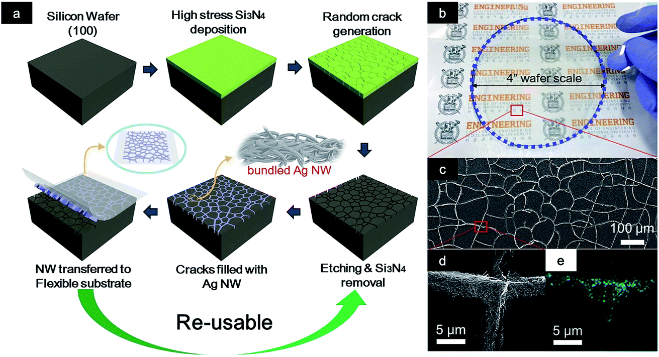 | ||
| Fig. 1 Fabrication of highly flexible and transparent bundled Ag nanowire networks (BANN) using template made from random cracking of thin film. (a) Schematic diagram of process. (b) Digital image of fabricated, highly flexible, transparent BANN in wafer scale. (c) SEM image of random network of BANN. (d) Magnified SEM image of BANN, and (e) corresponding EDS mapping of Ag element (cyan) at red box in (c). | ||
The generated random micro-cracks on a Si wafer are filled with the Ag NW ink to form the BANN electrode inside the random cracks. The Ag NW ink solution is advantageous for filling the random cracks and reducing total material usage. The BANN in the random crack can be successfully transferred to a transparent and flexible PET substrate after UV curable epoxy resin is applied and cured to promote adhesion between the BANN and substrate. Since the adhesion between the BANN and the cured epoxy resin is much greater than simple van der Waals force to the Si substrate, the bundled Ag NWs in the random crack patterns are faithfully transferred to the polymer film (Fig. 1c). As shown in Fig. 1b, the electrode on a PET film with transferred bundled Ag NW percolation networks along the random crack patterns is highly transparent and flexible while maintaining good electrical conductivity. The SEM image of the transferred BANN electrode on a PET film in Fig. 1c and d shows a multiscale BANN structure that consists of microscale wide random networks of nanometer-diameter wires. As verified in the EDS mapped image (Fig. 1e), the Ag NWs, indicated by Ag peaks (cyan), form junction networks within micro-cracks with less than 5 μm linewidth. Utilizing this multiscale structure of nanoscale bundles of nanowire networks within microscale random cracks shows superior optical, electrical and mechanical characteristics. As compared to the equally facile, transparent conductor fabrication process, for bar-coated or randomly dispersed nanowire percolation networks, transmittance increases at the cost of loss in electrical conductivity because the total conducting material coverage area is reduced. Detailed comparisons between BANN and bar-coated networks regarding achievable transmittance per used amount of NW are shown in the ESI, Fig. S2.† In addition, since the multiscale structure consists of a metal nanowire bundle, higher mechanical stability against bending is anticipated than the conventional metal networks made by sputtering or evaporation.
Since the cracks are induced by the residual stress of the Si3N4 film that occurs in a wafer scale regardless of size,26 as shown in Fig. 2a, an entire wafer can be patterned by random cracks without any conventional photolithographic processing; consequently, no additional patterning step is required. The initial linewidth of the crack patterns is in nanoscale (100–150 nm), which is equivalent to patterns made by state-of-the-art patterning techniques, yet no complicated masks or aligning steps are required. Furthermore, this nanoscale width can be easily widened by an isotropic etchant such as HNA. Since the etching rate of the Si3N4 is much less than that of Si crystal,22,23 the Si3N4 film can be used as a further etch mask. Depending on the time and concentration of the HNA solution, total etch time, width and surface roughness vary.24 As shown in Fig. 2b, various concentrations of the HNA solution were tested for optimization of a smooth cross-section profile. For template fine surface, relatively less HF content than HNO3 is required, and the higher H2O content enables finer control of etch width. Beginning with the nano-size pattern width, template pattern width can be broadly controlled from several hundred nanometers to several hundred micrometers.
 | ||
| Fig. 2 Wafer-scale, random nano-crack generation and characteristics of micro-channels widened from nano-cracks by post wet etching. (a) Random cracks generated in wafer scale (top). Initial generated random nano-cracks (middle) and widened micro-cracks after wet etching (bottom). (b) Etching rate of cracks for different HNA mixing ratios. Note that surface profiles vary by HF content in solution. Insets (right) show channels filled with BANN (high-resolution image included in ESI Fig. S1†). (c) SEM images of transferred patterns on UV curable polymer from random crack template on Si wafer after multiple times of use. Cross-sectional SEM images of (d), typical random micro-crack after optimized wet etching and (e), transferred Ag NW bundled networks (magnified surface shows BANN in inset image) on UV curable polymer, and (f), its corresponding EDS mapped image showing silver nanowires on surface in yellow peak. | ||
The hard silicon template enables repetitive use of the crack patterns for replication on UV curable polymer. Fig. 2c shows the template after 10 uses, yet no damage by the blading process during nanowire filling into the template was observed. Fig. 2d shows a cross-sectional view of the micro-crack channel from etching nano-crack channel with the optimized HNA solution. As shown in Fig. 2e, the Ag NW bundles were transferred to the replicated polymer patterns. The BANN formed in the random micro-crack template is successfully transferred onto the surface of the epoxy resin, as verified in a yellow color peak in the EDS mapped image, shown in Fig. 2f.
Although precise crack control of random fractures is not performed as in previous studies,16 random crack grid density as well as pattern width control, which are essential parameters closely related to properties of a transparent conductor, were performed. The grid density, equivalent to random crack area density since a closed area is made by an individual crack domain, can be controlled by crack initiation rate. There are various possible techniques to induce a higher crack initiation rate such as addition of artificial defects; however, the simplest method is to increase thickness of the Si3N4 film. As shown in Fig. 3a, assuming that an area closed by random cracks is a grid size, the template made by thinner Si3N4 film corresponds to a larger average grid size. As the Si3N4 film thickness is increased, the average grid size decreases and grid size variation is reduced. As shown in the probability distribution in Fig. 3b, the envelope of the distribution diminishes and a sharp peak appears as the Si3N4 film thickness is increased above 2 μm. Mean values of each distribution correspond to average grid size. For the Si3N4 film thicknesses 1.65 μm, 1.85 μm, 1.95 μm, and 2.05 μm, the corresponding average grid sizes are 7.6 × 103 μm2, 34 × 103 μm2, 56 × 103 μm2, and 340 × 103 μm2, respectively. As shown in Fig. 3c, the average grid size exponentially decreases as the Si3N4 film thickness is increased. The limiting factor for lowering average grid size is delamination of the Si3N4 film as film thickness greater than ∼3 μm yields to severe delamination failure.
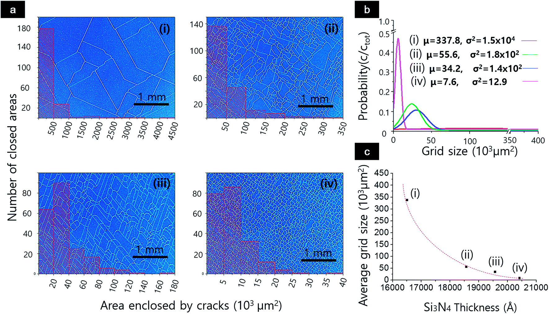 | ||
| Fig. 3 Control of random crack density generated by residual stress of Si3N4 thin film. (a) Optical microscope images along with crack domain area distribution at different random crack densities. Note that crack density increases from (i) to (iv). (b) Probability distribution of random crack domain area for corresponding cases (i–iv) in (a). (c) Graph of Si3N4 film thickness versus average crack domain area for corresponding cases (i–iv) in (a). | ||
The optical transmittance of the random BANN transparent and flexible conductor transferred to a PET film is shown in Fig. 4a. Although the transmittance and density of the crack or linewidth of the cracks have an inversely proportional relationship, the BANN linewidth is kept at 7 μm for simplicity. Transmittance of the BANN transparent conductor for a given linewidth fabricated from random crack template with the highest crack density (7.6 × 103 μm2 average grid size) is above 85% at 550 nm wavelength. Obviously, there is a tradeoff between optical transmittance and sheet resistance since the number of networks created by the random crack governs sheet resistance. As shown in Fig. 4b, the minimum sheet resistance is 92 Ω sq−1 for the high-density sample (see ESI, Fig. S2† for sheet resistance distribution). The sheet resistance exponentially increases as grid size increases. No moiré is observed since all the networks are in random shapes.
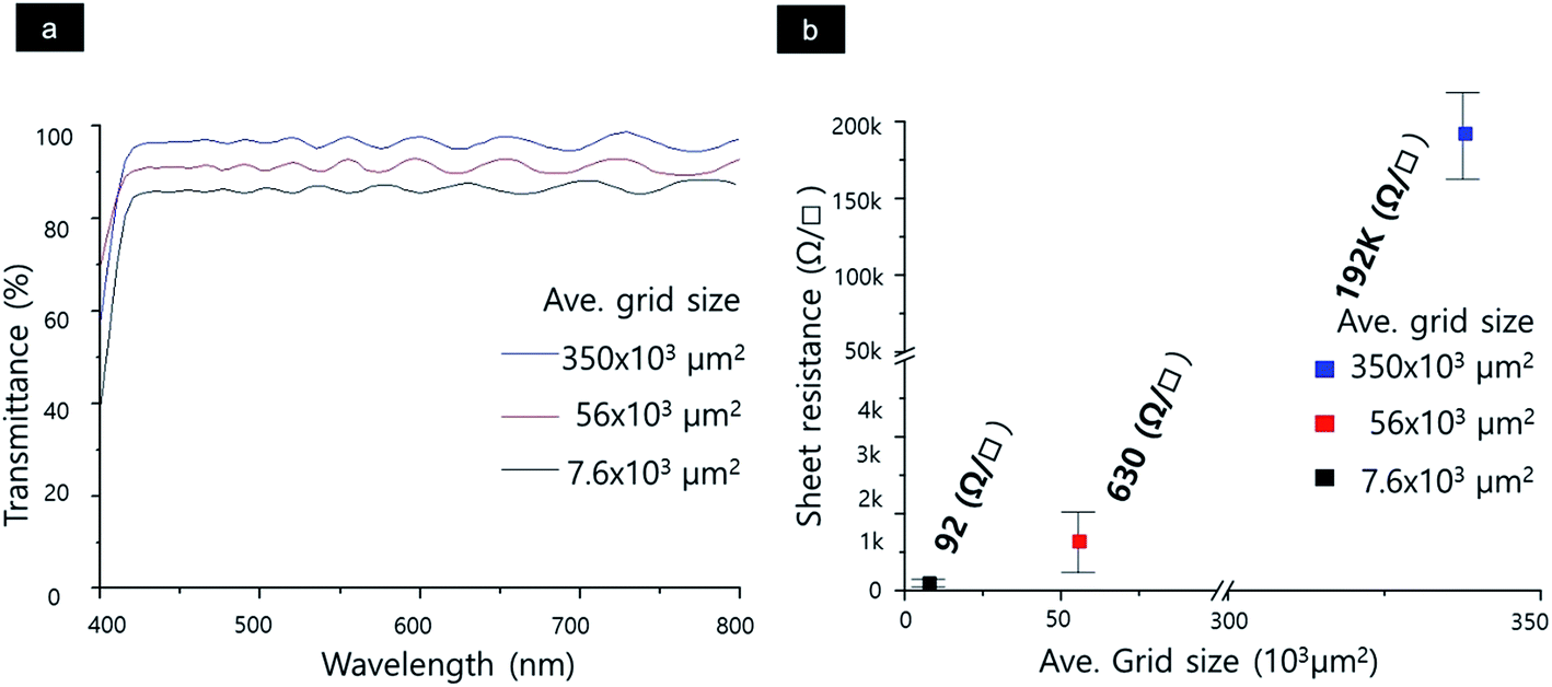 | ||
| Fig. 4 Optical and electrical characteristics of transparent conductor fabricated from BANN transferred onto PET film. (a) Spectral transmittance for various crack domain areas. (b) Sheet resistance for various crack domain areas. | ||
The flexible and transparent BANN electrode shows good mechanical reliability under repeated bending. This may be due to enhanced mechanical properties of bundled nanowire network as well as good adhesion between the nanowires and the PET substrate. As shown in Fig. 5a, after over 5000 cyclic bends, relative sheet resistance change (R/R0) is less than 15% in tensile bending (convex) and 6% in compressive bending (concave) at 15 mm bending radius, which commercial ITO/PET film fails to withstand after several tens of bending cycles.25 Even under extreme conditions12 (under 1 mm bending radius or 50000 cycles at 3.5 mm bending radius), outstanding mechanical performance has been demonstrated (see ESI, Fig. S5 and S6†). Through a simple transfer process, a flexible transparent conductor of wafer size was readily prepared as shown in Fig. 5b. It substantiates that the size of the resultant transparent conductor is directly proportional to the size of the underlying wafer, showing potential scalability of this process. As shown in Fig. 5c, we further confirmed that the transparent conductor fabricated in this manner can be directly used as a touch-screen panel application. Different from typical metal NW percolation network, the bundled metal NW percolation network electrodes are not susceptible to the detachment or physical damage that might arise during resistive touch-screen panel operation, thus no performance degradation due to wearing out is anticipated.
 | ||
| Fig. 5 Mechanical characterization and highly flexible touch panel demonstration of transparent BANN electrode fabricated from random crack template. (a) Tensile (top) and compressive (bottom) cyclic bending test of transparent conductor at 15 mm bending radius with 5000 cycles. (b) Highly flexible, wafer-scale touch-screen panel fabricated using high-density random crack template. Note that no moiré appears in panel. (c) Touch-screen demonstration with fabricated transparent conductor. | ||
4. Conclusions
In this paper, we propose a novel scheme to prepare bundled-metal NW, percolation network-based, flexible transparent conductor with enhanced mechanical robustness, yet without the moiré pattern problem. Metal NWs are used as the constituent building blocks to exploit their superior mechanical and electrical properties, but in bundles at microscale to enhance overall mechanical stability. The template patterns for metal NW bundle transfer on the flexible substrates are generated by using random crack generation of silicon nitrate film deposited on a silicon substrate as the mold. We found that this strategy offers a number of advantages. (1) The mold can be used repeatedly to yield identical transparent conductor at high reproducibility. (2) The density and linewidth of the metal NW bundles—hence, the optical transparency and electrical conductivity of the resultant transparent conductor—can be separately controlled through varying film thickness or changing the etching parameters without incorporating any complex photolithography process. (3) Having a random nature, the resultant transparent conductors are free from the moiré pattern problem. (4) Since the cracking occurs uniformly over the entire silicon wafer regardless of size, a large-area transparent conductor can be easily manufactured by a simple transfer process, whereas the size subject to the single process is expected to be further extended simply by employing a larger silicon wafer. By applying the resultant transparent conductor to a touch-screen display, we substantiate that this process possesses great potential as a new scheme for manufacture of novel flexible transparent conductors.Specific author contributions
Y. D. S., S. H., J. Y. and S. H. K. designed the experiments. J. L., H. L. and H. M. synthesized the materials. Y. D. S., P. W. and J. K. prepared the sample. H. L., S. J. and H. M. performed materials characterization of the sample. Y. D. S., S. H., J. Y. and S. H. K. co-wrote the manuscript.Acknowledgements
This work is supported by the National Research Foundation of Korea (NRF) (grant 2012-0008779); Global Frontier R&D Program on Center for Multiscale Energy System (grant 2012-054172); Nano-Material Technology Development Program (R2011-003-2009) funded by the Ministry of Science, ICT & Future; R&D Convergence Program, R&D program of MSIP/COMPA (grant 2015K000216); and Institute of Advanced Machinery and Design at Seoul National University (SNU-IAMD).Notes and references
- C. G. Granqvist, Transparent conductors as solar energy materials: A panoramic review, Sol. Energy Mater. Sol. Cells, 2007, 91, 1529–1598 CrossRef CAS.
- A. R. Madaria, A. Kumar and C. Zhou, Large scale, highly conductive and patterned transparent films of silver nanowires on arbitrary substrates and their application in touch screens, Nanotechnology, 2011, 22, 245201 CrossRef PubMed.
- S. Hong, et al., Highly Stretchable and Transparent Metal Nanowire Heater for Wearable Electronics Applications, Adv. Mater., 2015, 27, 4744–4751 CrossRef CAS PubMed.
- J. Kang, et al., High-performance graphene-based transparent flexible heaters, Nano Lett., 2011, 11, 5154–5158 CrossRef CAS PubMed.
- Y. Shigesato, R. Koshi-Ishi, T. Kawashima and J. Ohsako, Early stages of ITO deposition on glass or polymer substrates, Vacuum, 2000, 59, 614–621 CrossRef CAS.
- T. Kawashima, H. Matsui and N. Tanabe, New transparent conductive films: FTO coated ITO, Thin Solid Films, 2003, 445, 241–244 CrossRef CAS.
- S. I. Na, S. S. Kim, J. Jo and D. Y. Kim, Efficient and flexible ITO-free organic solar cells using highly conductive polymer anodes, Adv. Mater., 2008, 20, 4061–4067 CrossRef CAS.
- H. Wu, et al., Electrospun metal nanofiber webs as high-performance transparent electrode, Nano Lett., 2010, 10, 4242–4248 CrossRef CAS PubMed.
- J. Y. Lee, S. T. Connor, Y. Cui and P. Peumans, Solution-processed metal nanowire mesh transparent electrodes, Nano Lett., 2008, 8, 689–692 CrossRef CAS PubMed.
- J. Yeo, et al., Next generation non-vacuum, maskless, low temperature nanoparticle ink laser digital direct metal patterning for a large area flexible electronics, PLoS One, 2012, 7, e42315 CAS.
- J. Lee, et al., Very long Ag nanowire synthesis and its application in a highly transparent, conductive and flexible metal electrode touch panel, Nanoscale, 2012, 4, 6408–6414 RSC.
- S. Nam, et al., Ultrasmooth, extremely deformable and shape recoverable Ag nanowire embedded transparent electrode, Sci. Rep., 2014, 4, 4788 Search PubMed.
- B. Han, et al., Uniform self-forming metallic network as a high-performance transparent conductive electrode, Adv. Mater., 2014, 26, 873–877 CrossRef CAS PubMed.
- R. Gupta, et al., Spray Coating of Crack Templates for the Fabrication of Transparent Conductors and Heaters on Flat and Curved Surfaces, ACS Appl. Mater. Interfaces, 2014, 6, 13688–13696 CAS.
- K. Rao, R. Gupta and G. U. Kulkarni, Fabrication of Large Area, High-Performance, Transparent Conducting Electrodes Using a Spontaneously Formed Crackle Network as Template, Adv. Mater. Interfaces, 2014, 1, 140090 Search PubMed.
- K. H. Nam, I. H. Park and S. H. Ko, Patterning by controlled cracking, Nature, 2012, 485, 221–224 CrossRef CAS PubMed.
- E. Gorokhov, V. Y. Prinz, A. Noskov and T. A. Gavrilova, Novel Nanolithographic Concept Using Crack-Assisted Patterning and Self-Alignment Technology, J. Electrochem. Soc., 1998, 145, 2120–2131 CrossRef CAS.
- R. Elliman, M. Spooner, T. Dall, T. Kim and N. Fletcher, Oscillating cracks in glassy films on silicon substrates, Philos. Mag., 2007, 87, 4893–4906 CrossRef CAS.
- J. Lee, I. Lee, T. S. Kim and J. Y. Lee, Efficient Welding of Silver Nanowire Networks without Post-Processing, Small, 2013, 9, 2887–2894 CrossRef CAS PubMed.
- T. Ye, Z. Suo and A. Evans, Thin film cracking and the roles of substrate and interface, Int. J. Solids Struct., 1992, 29, 2639–2648 CrossRef.
- J. Li, et al., The role, mechanism and potentially novel biomarker of microRNA-17-92 cluster in macrosomia, Sci. Rep., 2015, 5, 17212 CrossRef CAS PubMed.
- K. R. Williams and R. S. Muller, Etch rates for micromachining processing. Microelectromechanical Systems, J. Microelectromech. Syst., 1996, 5, 256–269 CrossRef CAS.
- G. T. Kovacs, N. I. Maluf and K. E. Petersen, Bulk micromachining of silicon, Proc. IEEE, 1998, 86, 1536–1551 CrossRef CAS.
- A. Hamzah, et al., Optimization of HNA etching parameters to produce high aspect ratio solid silicon microneedles, J. Micromech. Microeng., 2012, 22, 095017 CrossRef.
- H. Lin, S. Chiu, T. Cho and J. Huang, Improved bending fatigue behavior of flexible PET/ITO film with thin metallic glass interlayer, Mater. Lett., 2013, 113, 182–185 CrossRef CAS.
- Y. D. Suh, et al., Control and Manipulation of Nano Cracks Mimicking Optical Wave, Sci. Rep., 2015, 5, 17292 CrossRef CAS PubMed.
Footnotes |
| † Electronic supplementary information (ESI) available. Additional information on the random cracks and bundled nanowire networks. See DOI: 10.1039/c6ra11467a |
| ‡ Y. D. S. and S. H. contributed equally to this work. |
| This journal is © The Royal Society of Chemistry 2016 |