DOI:
10.1039/C6QM00175K
(Research Article)
Mater. Chem. Front., 2017,
1, 922-927
The synthesis of a gold nanodisk–molecular layer–gold film vertical structure: a molecular layer as the spacer for SERS hot spot investigations†
Received
16th August 2016
, Accepted 21st November 2016
First published on 8th December 2016
Abstract
The objective of this research is to conduct a systematic measurement of hot spots formed between a gold (Au) nanodisk and an Au film using surface-enhanced Raman scattering (SERS). The dip-pen nanolithography and wet etching methods are used to fabricate sandwich structures with a self-assembled monolayer (SAM) or a polymer embedded between vertical Au nanodisks and the Au substrate. A flat polymer, which acts as a spacer, is synthesized via graft polymerization. The gap between the Au nanodisks and Au film is adjusted to the range from 2.4 to 12.1 nm by forming a SAM and repeating the graft polymerization. The SERS molecules, 4-mercaptobenzoic acid, are chemically bonded to the sidewalls of the Au nanodisks in order to observe the coupling interaction in the dipole of SERS while changing the gap size. According to the experimental results, the degree of field enhancement is greatly dependent on the dimensions of the gap. The greatest enhancement is reached when the gap distance is 3.8 nm, and no coupling effect is observed when the gap distance is more than 12 nm.
1. Introduction
With the advancements in technology, microminiaturization has become a major field of competition in the electronic devices manufacturing industry. The optimal way to produce nanoscale electronic products is to further diminish the size of the integrated circuits and fit more components into a limited space. Therefore, the primary goal of the industry is to develop more advanced manufacturing processes by which much smaller components for various applications can be produced. Several novel lithographic technologies, such as microcontact printing,1,2 e-beam lithography,3,4 and dip-pen nanolithography (DPN),5,6 have been developed in recent years. In DPN, developed by the Mirkin Group, the tip of the atomic force microscope (AFM) is utilized to form molecular patterns. The tip, coated with various molecules, such as organic molecules, nanoparticles, or biomolecules, approaches the substrate and transfers the molecules to the substrate surface through the meniscus formed by capillarity. Using this technique, the interfacial characteristics of the substrate surface can be modified, and molecular features in the nanometer range can be established. Because its action is exceedingly similar to pen writing, this technology is called direct writing nanolithography. Since the development of DPN, its utilization has been extended to a variety of applications, such as molecular circuits and biochips.7–9 Through its use, graphical self-assembled monolayers (SAMs) can be directly produced on the substrate surface and the functionality of that surface changed. A number of studies have focused on investigating the properties and the appropriate selection of substrates, molecules, and various chemical modifications to the prepared molecular patterns. For example, to produce metal nanoarrays, mercaptohexadecanoic acid (MHA) molecular patterns can be formed on a gold (Au) substrate via DPN technology, followed by wet etching.10–13
When the size of the metal materials is reduced to the nanoscale, they may obtain unique characteristics, such as surface plasmon resonance14–18 and surface-enhanced Raman scattering (SERS).19–23 Besides the SERS phenomenon caused by surface plasmon of noble metals, the plasmon-coupled interaction may occur when small gaps exist between two electrodes. As electromagnetic waves are transmitted within this small gap, a strong magnetic field may arise and increase the intensity of the Raman scattering of the molecules. Based on this phenomenon, a newly developed synthesis method for the production of 3D-vertical sandwich structures was conducted in this study to explore the coupling effect of gaps between metal electrodes. Initially, SAMs were embedded onto the Au substrate, and the gaps were formed by using graft polymerization reactions on the terminal functional groups of SAMs. Thermal evaporation was then applied to deposit the second Au layer on top of the polymer. With DPN technology, molecular patterns can be formed on the second Au layer, and the polymer can act as both the etching barrier and the spacer. Finally, the area without molecular patterns can be removed via wet etching for the preparation of Au nanodisks of various sizes. The thickness of the spacer between two electrodes can be controlled through polymerization with various reaction times and reagent concentrations. MHA with a –COOH terminal functional group was used as the DPN ink in this study, along with a monolayer spacer with a –SH head group. The test results were then compared with the SERS characteristics of 4-mercaptobenzoic acid (4MBA) adsorbed onto a bare Au substrate and an Au nanoarray on Si substrates. In this investigation, via the highly flexible DPN technology and synthetic processes, 3D components with hot spots, such as the sandwich structures shown in Fig. 1, were successfully prepared.
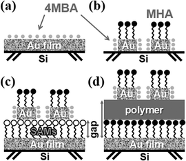 |
| | Fig. 1 Schematic representation of the SERS probe of 4MBA adsorbing (a) on the surface of the Au film and on the sidewall of the (b) Audisk array, (c) Audisk/SAM array, and (d) Audisk/polymer/SAM array. | |
2. Experimental
2.1 Materials
MHA (90%, Sigma-Aldrich) was used as the molecular ink for the DPN to pattern the Au surface. 1-Octadecanethiol (ODT; 98%, Sigma-Aldrich) was utilized for passivation. N-(3-Dimethylaminopropyl)-N′-ethylcarbodiimide hydrochloride (EDC; reagent grade, Sigma-Aldrich), N-hydroxysuccinimide (NHS; 98%, Sigma-Aldrich), cysteamine (95%, Sigma-Aldrich), and 2-(N-morpholino)ethanesulfonic acid (MES; 99.5%, Sigma-Aldrich) were used for the modification of the terminal functional group of MHA SAMs. Dimethylformamide (95%, Echo), dichloromethane (99%, Echo), benzene (95%, Fisher), ethyl acetate (95%, Echo), N-methylmorpholine (99%, Alfa Aesar), isobutyl chloroformate (98%, Alfa Aesar), p-toluenesulfonic acid monohydrate (98%, Sigma-Aldrich), 4,4′-azobis(4-cyanovaleric acid) (98%, Sigma-Aldrich), 1,4-dioxane (99.9%, Tedia), tert-butyl acrylate (99%, Alfa Aesar), 1,1′-carbonyldiimidazole (reagent grade, Sigma-Aldrich), and ethylenediamine (99%, Sigma-Aldrich) were used for the synthesis of surface-grafted polymer films. Ferric nitrate·9-hydrate (98%, J.T. Baker) and thiourea (99%, Sigma-Aldrich) were utilized as wet etching reagents. 4MBA (90%, Sigma-Aldrich) was chosen as the SERS probe. All chemicals obtained were used as received without further purification.
2.2 Preparation of Au substrates
A Si(100) wafer was cut into 0.5 × 1 cm2 pieces and ultrasonicated consecutively with hexane, ethanol, and deionized water for 20 min, followed by blow-drying with N2. The substrates were coated with a 6 nm chromium adhesion layer, followed by a 50 nm Au coating, at a rate of 0.1 Å s−1 by thermal evaporation with a base pressure of 1 × 10⁻⁶ Torr. The substrates subjected to the DPN process were tested within a week.
2.3 DPN and wet etching process
DPN experiments and sample imaging were carried out in an ambient environment (∼70% relative humidity, ∼298 K) using a multimode AFM (CP-II, Veeco) along with commercial DI-nanolithography software. In a typical experiment, all patterning works were performed using an MHA-coated tip, prepared by immersing a Si3N4 tip (SiNi, Budget Sensors) into an acetonitrile solution saturated with MHA for 10 s. The AFM tip was then dried with compressed N2. The pre-designed molecular patterns were generated by traversing the coated tip over the Au surface. With molecular dot patterns used as the etching barrier, the substrate was immersed in the ferric nitrate·9-hydroxide/thiourea mixed solution to form an Au nanodisk array by etching the sites without protection.
2.4 Preparation of Au nanodisks
By referring to the literature, molecular dot patterns can be produced via the DPN process on an Au film, followed by wet etching to remove the gold without the protection of the MHA.11–13 The sample prepared using this process, shown in Fig. 1b, is called Audisk.
2.5 Preparation of Au nanodisks on SAMs/Au substrates
After soaking the Au substrate in an MHA ethanolic solution overnight, the substrate was reacted with an MES aqueous solution (0.1 M) containing EDC/NHS (50/25 mM) at pH = 6. Cysteamine was then used to modify its terminal functional group into –SH.24,25 The second layer of a 50 nm Au film was deposited onto the substrate by thermal evaporation followed by DPN and wet etching for the preparation of Au nanodisks on SAMs (Audisk/SAM), as depicted in Fig. 1c.
2.6 Preparation of Au nanodisks on polymer/SAMs/Au substrate
For the graft polymerization, the Au substrate was immersed in an MHA ethanolic solution overnight, followed by the grafting process reported in other studies.26,27 To enhance the adhesion between the second evaporated Au film and the polymer, the hydrolysis of diamine–PTBA was carried out in the saturated p-toluenesulfonic acid benzene solution at 50–60 °C for 1 h to achieve the formation of polyacrylic acid (PAA) on the polymer surface. After PAA was formed, it was able to react with EDC/NHS and cysteamine producing –SH functional groups on the surface of the polymer. A 50 nm Au film was then deposited by thermal evaporation, followed by DPN and wet etching, to prepare the Au nanostructure array on the polymer–SAMs–Au substrate (Audisk/poly/SAM), as illustrated in Fig. 1d.
2.7 Characterization
In this study, AFM was used to scan the topography of a sample and to measure the thickness of a polymer film. SERS was acquired from a micro-Raman spectrometer (MonoRa 500i) using a 532 nm laser (power: 70 mW). The laser beam was focused on a spot approximately 1 μm2 in diameter, and the number of accumulated scans was set at 20. A scanning electron microscope (SEM; Hitachi S-4700) was used to observe the surface morphology of the samples.
3. Results and discussion
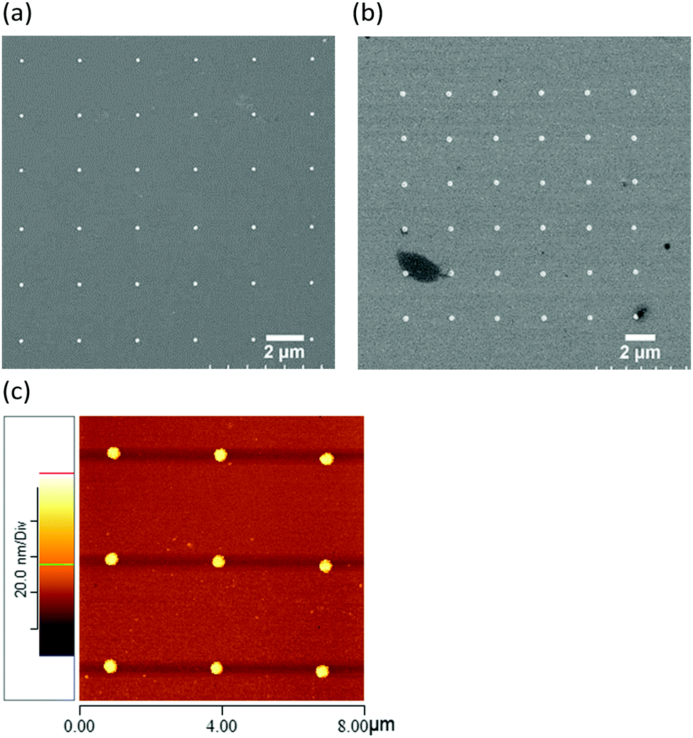
In this study, DPN technology was applied to form molecular dot patterns on an Au substrate, followed by wet etching to prepare an Au nanodisk array by removing the area lacking MHA molecules. This method can simplify the preparation of nanosized gold features regardless of the size and shape of the sample. To avoid laser exposure on more than one nanodisk in SERS measurements, the distance between each feature was maintained at no less than 2 μm. The Au film, with a thickness of 50 nm, was prepared by thermal evaporation. Fig. 2a shows the SEM image of the 6 × 6 Audisk array of Au nanodisks with a diameter of 180 nm. The size of these Au nanodisks is relatively uniform, and the etched areas are considerably smooth, resembling those described in the literature.11 This reveals that the MHA monolayer can be used as a resistant, and it remains on the gold nanodisks after the wet chemical etching process. This nanoarray can be utilized to observe the SERS phenomena resulting from the adsorption of the molecular probe on the sidewall of the gold nanodisks.
 |
| | Fig. 2 SEM images of (a) a 6 × 6 Audisk array with a diameter of 180 nm for each nanodisk; (b) a 6 × 6 Audisk/SAM array with the vertical structure of Audisc–SCH2CH2NHCO(CH2)15S–Au film. The diameter of each nanodisk was 400 nm. (c) The AFM topography of the 3 × 3 Audisk/poly/SAM array in (b). | |
One of the SAMs' features is that it can form a dense, well-ordered molecular layer on a substrate. The length of the alkane chain and the type of the terminal functional group may affect the thickness of the molecular layer and the angle between the molecules and the substrate.28 MHA covering the Au substrate, reacting with EDC/NHS and cysteamine, converts the terminal functional groups of SAMs from –COOH to –SH on the Au film resulting in the formation of HSCH2CH2NHCO(CH2)15S–Au. The thickness of the molecular layer established using tapping mode AFM was 2.4 nm. Because the surface functional group of the SAMs was modified to –SH, the evaporated second Au film (50 nm in thickness) could be deposited on it to form an S–Au covalent bond. This S–Au covalent bond strengthened the adhesion between the SAMs and the second Au film. The measured root-mean-square (RMS) roughness values of the first and second Au films were 0.875 and 2.025 nm, respectively. This elevated roughness of the Au film can be attributed to the yield of a surface modification reaction that increases the irregularity of the second Au film on a –SCH2CH2NHCO(CH2)15S–Au film.29 Through DPN and wet-chemical etching, a 6 × 6 and a 3 × 3 Audisk/SAM array, in terms of an Au nanodisk–SCH2CH2NHCO(CH2)15S–Au film, were formed, and each nanodisk had a diameter of 400 nm, as shown in Fig. 2b and c. The nanostructures with high uniformity evidenced that the high-quality 3D vertical structure on the SAM coating substrate could be synthesized using this protocol. The I–V curve of the Au nanodisk–SAMs–Au film's molecular junction was measured to confirm that Au atoms could not penetrate the SAMs to reach the Au substrate (Fig. S1, ESI†). No short circuit was detected between the upper and lower Au layers, and the high resistance was considered to be normal for a metal–insulator–metal junction.30 Therefore, the synthesis process proposed in this study has a strong potential for the development of molecular circuits. By controlling the retention time of the AFM tip on the substrate, DPN technology can easily draw the required molecular pattern with a predetermined size. Au nanodisks of various diameters can also be prepared and used to observe the spatial effect on its Raman scattering.
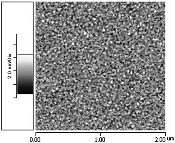
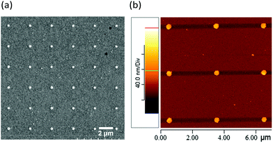
During the synthesis of the polymer spacer, the thickness of the polymer film was controlled and measured to verify the gap spacing following graft polymerization onto the Au substrate. The height of the spacer in this 3D nanostructure was measured through the MHA dot (diameter >2 μm) formed on the Au substrate using DPN, followed by the passivation of the area without MHA patterns, via ODT. The polymer was synthesized on these MHA patterns through graft polymerization, and the terminal functional groups were then modified to –SH. Based on AFM measurement, the thickness of the film was 1.8 (±0.15) nm after the first graft polymerization. For the second and third graft polymerization processes, the thickness of the film was 5.9 (±0.20) nm and 10.1 (±0.42) nm, respectively. The total spacer thickness was the thickness of the polymer plus the height of ODT (molecular height of ODT = 2 nm measured by AFM). Therefore, the gap spacing after one layer of graft polymerization was 3.8 nm and increased to 7.9 nm and 12.1 nm with two and three layers of polymers, respectively. Fig. 3 presents the AFM topography of the polymer film with a roughness RMS <0.1 nm, which is lower than that of the Au film deposited with thermal evaporation. This measurement indicates that an exceedingly flat polymer thin film can be formed using graft polymerization. Compared with other coating methods, such as dip coating, spin coating, or blade coating, graft polymerization requires the realization of additional organic synthesis steps. However, it also offers superior control of roughness and thickness of the polymer film compared to other methods. Therefore, it is suitable for the preparation of a nanosized gap.
 |
| | Fig. 3 2 × 2 μm2 AFM topography of a polymer film synthesized via graft polymerization. The roughness RMS was 0.067 nm. | |
After the flat polymer grew on the MHA covering the Au substrate, the surface functional group was modified to –SH. Thermal evaporation was then used to deposit the second Au film, followed by DPN and wet etching to create the vertical sandwich structure. The schematic representation of the Au nanodisk/polymer–SAMs/Au film is illustrated in Fig. 1d. In Fig. 4a, the SEM image of a 6 × 6 Audisk/poly/SAM array, in terms of an Audisc–SCH2CH2NHCO–polymer–CO(CH2)15S–Au film, indicates that the Au nanodiscs can be prepared on the second Au layer by repeating the above-mentioned DPN and wet etching processes. The diameter of the Au nanodisk was 350 nm, and the vertical distance between the Au nanodisk and the Au substrate was 7.9 nm. Based on the SEM and AFM images, it is clear that the Au nanodisk arrays can be successfully prepared on the Si, SAMs/Au, or polymer/SAMs/Au surfaces. Their sizes and spacing can also be easily controlled to observe the corresponding relationship of SERS with various vertical gap distances. Because of the versatile utility of DPN, the size of the Au nanodisk can be regulated through the scale of the molecular pattern, similar to the samples prepared in this study, with diameters of 180, 350, and 400 nm.
 |
| | Fig. 4 (a) An SEM image of a 6 × 6 Audisk/poly/SAM array. The diameter of each Au nanodisk was 350 nm and the gap between the Au nanodisks and the Au film was 7.9 nm. (b) The AFM topography of the 3 × 3 Audisk/poly/SAM array in (a). | |
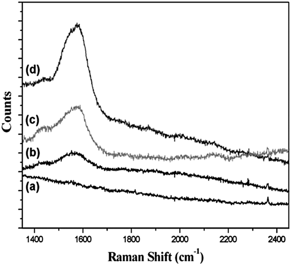
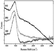
The diameter of each nanodisk used in the samples prepared for micro-Raman spectrometer measurements were limited to 350 and 700 nm to avoid the interference caused by the scale effect. The SERS spectra of 4MBA adsorbed on the sidewall of various Au structures, including the bare Au film, Audisk, Audisk/SAM, and Audisk/polymer/SAM, are shown in Fig. 5. To avoid displacement between the 4MBA molecules and the MHA on the nanodisk, the immersion time of the sample in the 4MBA ethanolic solution was limited to less than 10 min. The Raman signal of pure 4MBA powders was recorded at 1592 cm−1, which was attributed to the ν8a aromatic ring vibrations.31 The signal strength of the Audisk/SAM and Audisk/polymer/SAM substrates with a gap structure was higher than that of the Audisk and the bare Au film without a gap structure. For the bare Au film, the measured Raman scattering was relatively weak due to the lower degree of surface roughness and the absence of hot spots. For the structures with a gap, Audisk/polymer/SAM (gap = 3.8 nm) exhibited a stronger signal than that of the Audisk/SAM with SAMs.
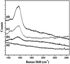 |
| | Fig. 5 SERS measurements with 4MBA as the probe with the substrate of (a) a bare Au film, (b) Audisk, (c) Audisk/SAM and (d) Audisk/polymer/SAM with gap thicknesses of 3.8 nm. Raman shift at 1580 cm−1 represents a ν8aC–Cring band of 4MBA. | |
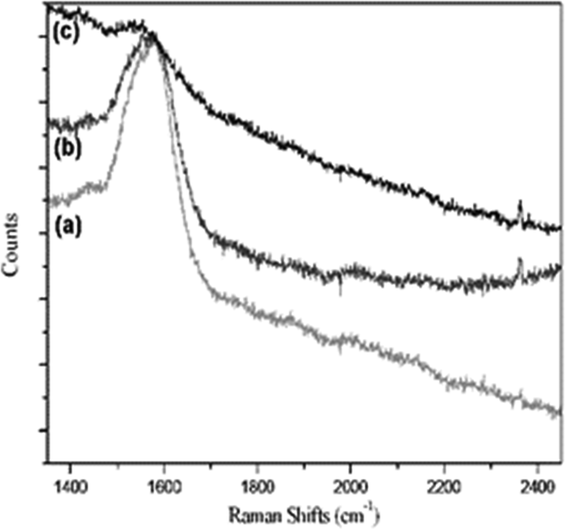
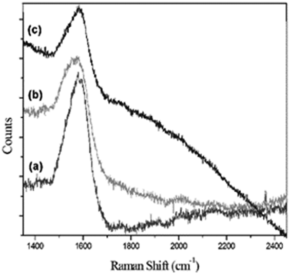
When conducting Raman scattering experiments on the metal arrays with 4MBA adsorption, a plasma resonance zone, known as hot spots, upon optical excitation, was formed by confining the gap between metal layers. In order to verify the SERS variation caused by the vertical distance, three different sandwich structures (350 nm Au nanodisks) with gap distances of 3.8, 7.9, and 12.1 nm were synthesized. The respective spectra are shown in Fig. 6. By evaluating the SERS counts, it was established that the vertical structure with single graft polymerization exhibited the highest enhancement when the gap was set to 3.8 nm, and its scattering decreased as the spacer thickness increased. Fig. 7 illustrates the SERS spectra of polymers with various thicknesses as a spacer, where the signal strength and trend of the 700 nm Audisk/polymer/SAM is remarkably similar to those of the 350 nm Audisk/polymer/SAM. The most obvious signal enhancement was found on the sample with the single graft polymerization with a spacer of 3.8 nm. Comparing these data with the ones presented in Fig. 6, it becomes clear that the Au nanoarray with the larger diameter (700 nm) can adsorb more molecular probes and produces a stronger Raman signal than the smaller array (350 nm). The relationship between SERS strength and gap thickness in other 3D structures is shown in Fig. 8.
 |
| | Fig. 6 SERS measurements with 4MBA as the probe and Audisk/polymer/SAM as the substrate. The diameter of the Au nanodisk was 350 nm with a gap size of (a) 3.8, (b) 7.9, and (c) 12.1 nm. | |
 |
| | Fig. 7 SERS measurements with 4MBA as the probe and Audisk/polymer/SAM as the substrate. The diameter of the Au nanodisk was 700 nm with a gap size of (a) 3.8, (b) 7.9, and (c) 12.1 nm. | |
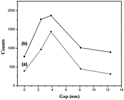 |
| | Fig. 8 The relationship between SERS strength and the gap of 3D structures. The diameter of the Au nanodisk was 350 and 700 nm in (a) and (b), respectively. | |
To verify the spatial effect on SERS, the corresponding enhancement factors (EFs) are calculated using the equation EF = (Isers/Nads)/(Ibulk/Nbulk).32–34 The calculated results are listed in Table 1. When a gap exists beneath an Au nanodisk, its EF is greater than that of an Audisk. For a spacer with a 3.8 nm gap, EFs of 2909 and 1890 were measured for nanodisks with diameters of 350 and 700 nm, respectively. As the gap increased beyond 12 nm, the EF decreased dramatically. According to the existing literature, a small gap between metallic nanomaterials may result in a coupling effect.35–40 Following exposure to radiation, a strong coupling could be caused with the applied electromagnetic field and, thus, the probability of Raman scattering of the molecules within the region is greatly increased. As shown in Table 1, when the gap is larger than ∼12 nm, the SERS signal of the Audisk/poly/SAM is similar to that of the Audisk (gap = 0). This means that Raman scattering results only from the adsorption of 4MBA on the sidewall of the Au nanodisks without the coupling effect.
Table 1 (a) The relationship between gap thickness, SERS counts, and the EFs of the Au nanodisk with a diameter of 350 nm. (b) The relationship between gap thickness, SERS counts, and the EFs of the Au nanodisk with a diameter of 700 nm
| (a) |
|
| Gap (nm) |
0 |
2.4 |
3.8 |
7.9 |
12.1 |
| SERS counts |
397 |
970 |
1439 |
451 |
312 |
| EFs |
802 |
1960 |
2909 |
911 |
631 |
|
|
| (b) |
|
| Gap (nm) |
0 |
2.4 |
3.8 |
7.9 |
12.1 |
| SERS counts |
780 |
1769 |
1870 |
1015 |
897 |
| EFs |
788 |
1788 |
1890 |
1026 |
906 |
4. Conclusions
In this study, we present an advanced method for combining DPN, wet chemical etching, chemical modification, and graft polymerization to synthesize a 3D vertical nanostructure for SERS observation. Two spacers, including SAMs and flat polymers, were modified and polymerized through chemical reactions and embedded between an Au nanodisk and Au film to form a metal–molecules–metal architecture. In SERS measurements, the highest coupling effect was observed with a gap of 3.8 nm, and it disappeared as the spacer became larger than ∼12 nm. The synthetic process proposed in this investigation has great potential in the production of electro-optical devices. In the next paper, we will present another facile method for preparing 3D metal–polymer–metal nanostructures using polypyrrole as the spacer and a probe for SERS measurement.
Acknowledgements
The authors thank the Ministry of Science and Technology of Taiwan for financial support (MOST 104-2623-E-027-001-D and MOST 105-2119-M-027-006). Y.-H. C. acknowledges Prof. Shih-Hui Chang (National Cheng Kung University) and Prof. Yit-Tsong Chen (National Taiwan University) for SERS spectra measurements and discussions.
References
- A. Kumar and G. M. Whitesides, Appl. Phys. Lett., 1993, 63, 2002–2004 CrossRef CAS.
- J. L. Wilbur, A. Kumar, E. Kim and G. M. Whitesides, Adv. Mater., 1994, 6, 600–604 CrossRef CAS.
- J. A. M. Sondag-Huethorst, H. R. J. van Helleputte and L. G. J. Fokkink, Appl. Phys. Lett., 1994, 64, 285–287 CrossRef CAS.
- P. M. Mendes, S. Jacke, K. Critchley, J. Plaza, Y. Chen, K. Nikitin, R. E. Palmer, J. A. Preece, S. D. Evans and D. Fitzmaurice, Langmuir, 2004, 20, 3766–3768 CrossRef CAS PubMed.
- R. D. Piner, J. Zhu, F. Xu, S. Hong and C. A. Mirkin, Science, 1999, 283, 661–663 CrossRef CAS PubMed.
- S. Hong, J. Zhu and C. A. Mirkin, Science, 1999, 286, 523–525 CrossRef CAS PubMed.
- L. Qin, S. Park, L. Huang and C. A. Mirkin, Science, 2005, 309, 113–115 CrossRef CAS PubMed.
- R. A. Vega, C. K.-F. Shen, D. Maspoch, J. G. Robach, R. A. Lamb and C. A. Mirkin, Small, 2007, 3, 1482–1485 CrossRef CAS PubMed.
- Y.-H. Chang and C.-H. Wang, J. Mater. Chem., 2012, 22, 3377–3382 RSC.
- H. Zhang, S.-W. Chung and C. A. Mirkin, Nano Lett., 2003, 3, 43–45 CrossRef CAS.
- K. S. Salaita, S. W. Lee, X. Wang, L. Huang, T. M. Dellinger, C. Liu and C. A. Mirkin, Small, 2005, 1, 940–945 CrossRef CAS PubMed.
- D. A. Weinberger, S. Hong, C. A. Mirkin, B. W. Wessels and T. B. Higgins, Adv. Mater., 2000, 12, 1600–1603 CrossRef CAS.
- J.-W. Jang, R. G. Sanedrin, A. J. Senesi, Z. Zheng, X. Chen, S. Hwang, L. Huang and C. A. Mirkin, Small, 2009, 5, 1850–1853 CrossRef CAS PubMed.
- S. S. Aćimović, M. P. Kreuzer, M. U. González and R. Quidant, ACS Nano, 2009, 3, 1231–1237 CrossRef PubMed.
- K. A. Willets and R. P. Van Duyne, Annu. Rev. Phys. Chem., 2007, 58, 267–297 CrossRef CAS PubMed.
- K.-H. Su, Q.-H. We, X. Zhang, J. J. Mock, D. R. Smith and S. Schultz, Nano Lett., 2003, 3, 1087–1090 CrossRef CAS.
- K. M. Mayer and J. H. Hafner, Chem. Rev., 2011, 111, 3828–3857 CrossRef CAS PubMed.
- D. J. Park, C. Zhang, J. C. Ku, Y. Zhou, G. C. Schatz and C. A. Mirkin, Proc. Natl. Acad. Sci. U. S. A., 2015, 112, 977–981 CrossRef CAS.
- K. L. Wustholz, A.-I. Henry, J. M. McMahon, R. G. Freeman, N. V. Valley, M. E. Piotti, M. J. Natan, G. C. Schatz and R. P. Van Duyne, J. Am. Chem. Soc., 2010, 132, 10903–10910 CrossRef CAS PubMed.
- J. Zhao, A. O. Pinchuk, J. M. McMahon, S. Li, L. K. Ausman, A. L. Atkinson and G. C. Schatz, Acc. Chem. Res., 2008, 41, 1710–1720 CrossRef CAS PubMed.
- J. P. Camden, J. A. Dieringer, J. Zhao and R. P. Van Duyne, Acc. Chem. Res., 2008, 41, 1653–1661 CrossRef CAS PubMed.
- G. Chen, Y. Wang, M. Yang, J. Xu, S. J. Goh, M. Pan and H. Chen, J. Am. Chem. Soc., 2010, 132, 3644–3645 CrossRef CAS PubMed.
- M.-H. Wang, J.-W. Hu, Y.-J. Li and E. S. Yeung, Nanotechnology, 2010, 8, 145608 CrossRef PubMed.
- Z. Grabarek and J. Gergely, Anal. Biochem., 1990, 185, 131–135 CrossRef CAS.
- D. Sehgal and I. K. Vijay, Anal. Biochem., 1994, 218, 87–91 CrossRef CAS PubMed.
- M. L. Bruening, Y. Zhou, G. Aguilar, R. Agee, D. E. Bergbreiter and R. M. Crooks, Langmuir, 1997, 13, 770–778 CrossRef CAS.
- Y. Zhou, M. L. Bruening, D. E. Bergbreiter, R. M. Crooks and M. Wells, J. Am. Chem. Soc., 1996, 118, 3773–3774 CrossRef CAS.
- J. Christopher Love, L. A. Estroff, J. K. Kriebel, R. G. Nuzzo and G. M. Whitesides, Chem. Rev., 2005, 105, 1103–1169 CrossRef PubMed.
- J. Lahiri, E. Ostuni and G. M. Whitesides, Langmuir, 1999, 15, 2055–2060 CrossRef CAS.
- C. Chu, J.-S. Na and G. N. Parsons, J. Am. Chem. Soc., 2007, 129, 2287–2296 CrossRef CAS PubMed.
- A. Michota and J. Bukowska, J. Raman Spectrosc., 2003, 34, 21–25 CrossRef CAS.
- A. D. McFarland, M. A. Young, J. A. Dieringer and R. P. Van Duyne, J. Phys. Chem. B, 2005, 109, 11279–11285 CrossRef CAS PubMed.
- K.-H. Su, S. Durant, J. M. Steele, Y. Xiong, C. Sun and X. Zhang, J. Phys. Chem. B, 2006, 110, 3964–3968 CrossRef CAS PubMed.
- E. C. Le Ru, E. Blackie, M. Meyer and P. G. Etchegoin, J. Phys. Chem. C, 2007, 111, 13794–13803 CAS.
- Y. Sawai, B. Takimoto, H. Nabika, K. Ajito and K. Murakoshi, J. Am. Chem. Soc., 2007, 129, 1658–1662 CrossRef CAS PubMed.
- S. Li, M. L. Pedano, S.-H. Chang, C. A. Mirkin and G. C. Schatz, Nano Lett., 2010, 10, 1722–1727 CrossRef CAS PubMed.
- D.-K. Lim, K.-S. Jeon, J.-H. Hwang, H. Kim, S. Kwon, Y. D. Suh and J.-M. Nam, Nat. Nanotechnol., 2011, 6, 452–460 CrossRef CAS PubMed.
- H. Im, K. C. Bantz, N. C. Lindquist, C. L. Haynes and S.-H. Oh, Nano Lett., 2010, 10, 2231–2236 CrossRef CAS PubMed.
- L. Qin, S. Zou, C. Xue, A. Atkinson, G. C Schatz and C. A. Mirkin, Proc. Natl. Acad. Sci. U. S. A., 2006, 103, 13300–13303 CrossRef CAS PubMed.
- S. Kessentini, D. Barchiesi, C. D'Andrea, A. Toma, N. Guillot, E. D. Fabrizio, B. Fazio, O. M. Marago, P. G. Gucciardi and M. L. de la Chapelle, J. Phys. Chem. C, 2014, 118, 3209–3219 CAS.
Footnote |
| † Electronic supplementary information (ESI) available. See DOI: 10.1039/c6qm00175k |
|
| This journal is © the Partner Organisations 2017 |
Click here to see how this site uses Cookies. View our privacy policy here. 
 *,
Wen-Hsin
Hsu
,
Song-Lun
Wu
and
Yung-Chin
Ding
*,
Wen-Hsin
Hsu
,
Song-Lun
Wu
and
Yung-Chin
Ding