 Open Access Article
Evaluation of different metal salt solutions for the preparation of solar cells with wide-gap Cu2ZnGeSxSe4−x absorbers†
T. Schnabel*,
M. Seboui and
E. Ahlswede
Zentrum für Sonnenenergie-und Wasserstoff-Forschung, Industriestraße 6, 70565 Stuttgart, Germany. E-mail: thomas.schnabel@zsw-bw.de
First published on 7th November 2016
Abstract
In this work, thin-film solar cells with a kesterite-type Cu2ZnGeSxSe4−x (CZGSSe) absorber were prepared from four different metal salt solutions. Their high band gap makes them an interesting material for tandem solar cells. The structural and morphological properties of the absorbers are compared with an additional focus on the electrical properties of the resulting thin-film solar cells. Efficiencies exceeding 5% could be demonstrated.
Introduction
In recent years the kesterite-type material Cu2ZnSnSxSe4−x (CZTS) has gained particular attention as an absorber material for thin-film solar cells. It offers a tunable band gap between 1.0 and 1.5 eV that can be adjusted via the S/Se-ratio. However, if one wants to use a kesterite material as a top cell in tandem solar cells, this range of band gaps is still too low. Therefore a different approach is necessary to further increase the band gap.One possibility is the replacement of tin by germanium, which has a smaller ionic radius and can increase the band gap to values between 1.4 eV (Cu2ZnGeSe4, CZGSe1) and 2.0 eV (Cu2ZnGeS4, CZGS2). However, for solar cells with kesterite-type absorber Ge is mostly used only as a dopant in small quantities.3 Additionally, there are some reports about mixed Cu2ZnSn1−yGeySxSe4−x absorbers.4–6 Here the best results were obtained for y-values between 0.25 and 0.4 with efficiencies approaching or exceeding 10%.4,7,8 In these reports the efficiencies are strongly declining for y > 0.5 and no explicit values for pure Cu2ZnGeSxSe4−x (CZGSSe) have been reported. In addition, there are a few manuscripts that mostly focus on structural and optical properties of CZGSSe,1,9 one of them showing a J–V-characteristic with a diode-shape, but no solar cell parameters.10 For solar cells based on CZGS monograins an efficiency of 1.3% was achieved by Timmo et al.,11 which is the highest reported efficiency so far.
Solution-based approaches allow both simple process technologies and low deposition costs and are interestingly head-on with vacuum-based approaches in the case of kesterite solar cells.12 Hence, the scope of this manuscript is to investigate different metal salt solutions for the synthesis of CZGSSe absorbers. Their optical and morphological properties are discussed with a focus on their suitability for the use in thin-film solar cells, resulting in the highest reported power conversion efficiency for this material.
Experimental
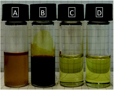
In this work four different metal salt solutions are compared. All of them were prepared with stoichiometries of Cu/(Zn + Ge) = 0.7 and Zn/Ge = 1.0, thus after a slight Ge-loss during annealing being in the Cu-poor and Zn-rich regime that has proven to be favourable for CZTS. The choice of solvent is motivated by both a good solubility of various metal salts and ideally by only little environmental impact: dimethyl sulfoxide (DMSO) – an established solvent for CZTS,13 N,N-dimethylformamide (DMF) as rather new candidate, and finally water. For solution A, copper(I)-acetate (0.45 M), zinc(II)-chloride (0.31 M), germanium(IV)-chloride (0.31 M) and thiourea (1.45 M) have been dissolved in DMSO. A turbid suspension is formed. The EDX-analysis of the precipitate showed S, O and Ge in different amounts. Solution B also has DMSO as solvent with copper(II)-acetate (0.44 M), zinc(II)-chloride (0.30 M) and germanium(IV)-iodide (0.30 M) as metal salts and thiourea (1.41 M) as sulfur-source.14 It forms a deep-red solution, which is clear when freshly prepared, but forms some precipitate over time. Solution C is prepared from copper(II)-oxide (0.31 M), zinc(II)-oxide (0.21 M) and germanium(IV)-oxide (0.21 M) that are solved in an aqueous solution of ammonium thioglycolate (ATG, 1.67 M). A clear, yellow solution is formed.15 Note that the solutions B and C are not prepared with Cu in the proper oxidation state for the kesterite lattice, which is +1. However, Cu(I) is formed through a redox reaction. Solution D consists of copper(I)-chloride (0.46 M), zinc(II)-chloride (0.32 M), germanium(IV)-chloride (0.31 M) and thiourea (1.48 M) that are dissolved in DMF and form a clear, yellow solution.4 A picture of all four solutions is displayed in Fig. 1.The metal salt solutions are deposited onto a Mo/soda lime glass substrate by doctor-blade coating and a subsequent drying step on a hot plate. The film thickness can be adjusted by the number of subsequent coating steps. Afterwards, the sample is annealed at approximately 550 °C inside a graphite box in selenium-atmosphere. Additional experimental details can be found in ref. 16. To obtain functional solar cells, the samples are completed with a CdS-layer (50 nm) by chemical bath deposition and a sputtered intrinsic ZnO (40 nm) and an aluminium-doped ZnO (400 nm) layer and separated to single cells of 0.25 cm2 each by mechanical scribing.
Current–voltage curves were measured using a Keithley 2400 source measuring unit under simulated AM 1.5 global solar irradiation with an WACOM 2-lamp sun simulator at 100 mW cm−2. External quantum efficiency measurements were performed with a setup from Optosolar. The morphology was investigated with a scanning electron microscope (SEM, XL30 SFEG Sirion) from FEI Company, using a 5 kV acceleration voltage. The same instrument was also used for energy-dispersive X-ray (EDX) measurements. Raman spectra were obtained by using a WITec CRM 200 confocal Raman microscope with a 532 nm excitation wavelength and a spot size of approximately 1 μm. X-ray diffraction (XRD) measurements were performed with the model Empyrean from Panalytical in Bragg–Brentano geometry.
Results
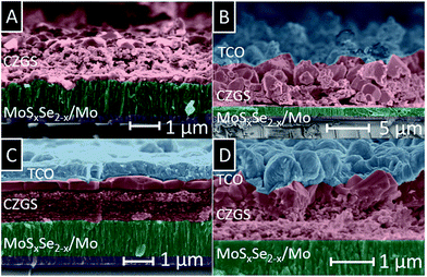
The morphologies of the samples from the metal salt solutions A–D are displayed in the SEM images in Fig. 2 and obviously show large differences. Sample A consists of small grains, only showing some larger crystals on the top and the bottom of the absorber. Additionally, an approximately 1 μm thick MoSxSe2−x-layer is visible, which is of comparable thickness for all samples. Sample B is even more inhomogeneous than sample A, showing some crystals that are considerably larger than the thickness of the other samples with smaller grains in between, but no compact layer was formed. Sample C shows a more homogeneous morphology with a large-grain layer on top and a thicker small-grain layer underneath. For sample D, a compact, but small-grain layer is visible with some larger grains on top.The crystallinity of the absorbers is examined by XRD, as shown in Fig. 3. The reference card for CZGSe is added in black bars (JCPDS 052-0867). All absorbers appear to have the kesterite structure and no secondary phases are visible. The only reflexes not belonging to CZGSSe comply with Mo and MoSe2. A more detailed plot of the 112- and the 202/204-reflex can be found in the ESI,† where a small amount of ZnSe was found for sample A. The reflexes are slightly shifted dependent on the S/(S + Se)-ratio, which can be estimated from the position of the 112-reflex via Vegard's law.17,18 This method shows that sample A has the lowest S/(S + Se)-ratio with 0.12 whereas especially the samples C and D have considerable S-incorporations with ratios around 0.3 (Table 1). These differences may be due to (i) a different reactivity of the S-containing substances (thiourea vs. ATG) for forming Cu2ZnGeS4 in the precursor, or (ii) due to differences in the compactness of the absorber layers, leading to an enhanced replacement of S by Se during the annealing process for a less compact layer.
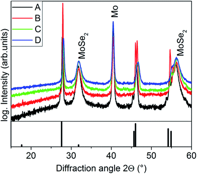 | ||
| Fig. 3 XRD spectra of absorbers prepared from the solutions A–D and reference card JCPDS 052-0867 for CZGSe. | ||
| Sample | A (DMSO) | B (DMSO) | C (water) | D (DMF) |
|---|---|---|---|---|
| 112-Position (°) | 27.799 | 27.914 | 28.043 | 28.095 |
| FWHM (°) | 0.267 | 0.164 | 0.267 | 0.361 |
| S/(S + Se) | 0.12 | 0.17 | 0.29 | 0.31 |
An indication for the crystal quality is the full width of half maximum (FWHM) of the XRD reflexes. Here sample B has with 0.164° by far the smallest value indicating larger crystals than for the other samples. This is in accordance with the SEM images shown in Fig. 2, where huge crystals can be found for sample B.
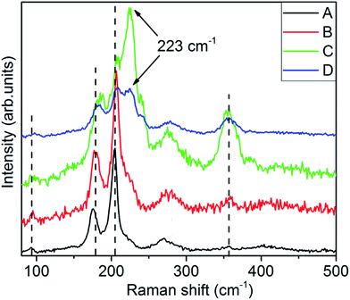
For additional investigations on the crystal structure Raman microscopy spectra are shown in Fig. 4. Here clear differences between the four absorbers are visible. First of all, all of them exhibit the A-modes for CZGSe at 205 and 177 cm−1 (ref. 19) and the A-mode for CZGS at 357 cm−1 (which is slightly red-shifted in comparison to the position observed by Guc et al. because of the high Se-content)20 and therefore the kesterite-structure is confirmed. However, the latter mode is barely visible for the samples A and B, complying with their lower S/(S + Se)-ratios as determined by XRD. Weaker kesterite modes can be seen at 93 and 270–290 cm−1, which is in agreement with previous reports, too.11,19,20
Interestingly, there is an additional mode at 223 cm−1 present for the samples C and D and as small shoulder for sample B; it varies in intensity (also on different spots on one sample) and is the strongest mode for sample C, while its origin is not clear at the moment. It was not observed for CZGSe single crystals21 but for CZGSSe thin films by Khadka et al.22 which suggests that it might be a kesterite-mode dependent on the S/(S + Se)-ratio. In general it is observed that the Raman modes for the samples A and B are clearly sharper than those for the samples C and D. So if we combine the information from XRD and Raman, we can conclude that from a structural point of view sample B shows the best crystal quality, while the samples C and D have a higher S/(S + Se)-ratio. Both of them have also a strong contribution of the unknown Raman mode at 223 cm−1.
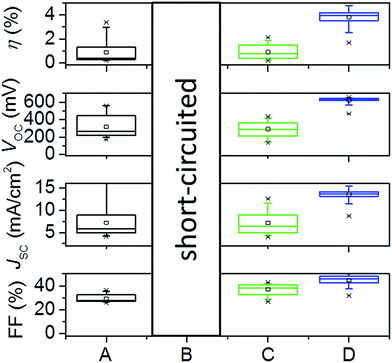
A totally different picture can be drawn from the solar cell parameters of the solar cells made from samples A–D, which are shown as boxplots in Fig. 5. The corresponding maximum and average values can be found in Table 2, detailed J–V characteristics are displayed in the ESI.† It is obvious that sample D exhibits the highest values for all parameters and at the same time a smaller deviation than the samples A and C. Sample B is short-circuited due to the lack of a compact layer that gives access to many shunt paths and does therefore not exhibit any efficiency. For sample A the maximum efficiency η is 3.6%, but it is very inhomogeneous and therefore has an average value of only 0.9%. Its average efficiency and short-circuit current density (Jsc) are comparable to sample C. Although the latter is more homogeneous it only shows a maximum efficiency of 2.1% that might be limited by the high amount of carbon residues that comes from the used complexant ATG.23 Due to the higher S/(S + Se)-ratio (see Table 1) the band gap of sample C (1.54 eV) is considerably larger.
| ηmax (%) | ηav (%) | VOC, max (mV) | VOC, av (mV) | JSC, max (mA cm−2) | JSC, av (mA cm−2) | FFmax (%) | FFav (%) | Eg (eV) | |
|---|---|---|---|---|---|---|---|---|---|
| A (DMSO) | 3.6 | 0.9 | 562 | 318 | 18.1 | 7.2 | 35.5 | 29.4 | 1.27 |
| B (DMSO) | N.A. | N.A. | N.A. | N.A. | N.A. | N.A. | N.A. | N.A. | N.A. |
| C (water) | 2.1 | 0.8 | 433 | 292 | 11.6 | 7.2 | 42.4 | 37.0 | 1.54 |
| D (DMF) | 5.1 | 3.8 | 615 | 621 | 16.3 | 13.6 | 50.7 | 44.6 | 1.50 |
Sample D is comparable to sample C in terms of band gap and S/(S + Se)-ratio. However, fill factor (FF), open-circuit voltage (VOC), JSC and therefore also the efficiency η are considerably higher reaching up to 5.1% with a VOC of 615 mV, JSC of 16.3 mA cm−2 and a FF of 50.7%. Note that the average VOC of sample D is higher than the one of the best cell.
The differences between the four approaches in this manuscript in terms of efficiency cannot be explained by an isolated comparison of the used solvents. Instead, the combination of solvent, metal salts and sulfur-source has to be taken into account, which results in a complex interplay.
If one wants to judge on the solvent alone, the requirements for being a suitable solvent include e.g. (i) offering a high solubility for the used metal salts, (ii) not leaving any residues in the final absorber layer and (iii) having a sufficient wettability on Mo-substrates to obtain homogeneous layers.
With respect to these criteria, the solutions based on DMSO could not demonstrate their easiness known from tin-based CZTS kesterites16 and unfortunately suffer from instable solutions and inhomogeneous film formation. The water based ATG approach facilitates stable “green” solutions and good film formation, but is limited in terms of efficiency due to huge carbon residues as mentioned above.
In contrast, the DMF approach fulfills all of the above-mentioned requirements. It allows the smallest amount of carbon, since no acetates or ATG were used and therefore thiourea is the only carbon-containing substance. Although less environmentally friendly than water-based solutions, solution D is stable for several weeks and homogeneous samples can be prepared making it the most promising approach of the four solutions discussed.
Conclusions
Cu2ZnGeSxSe4−x absorber layers have been prepared from four different metal salt solutions by a simple non-vacuum process. All approaches resulted in kesterite-type structures, but their morphology and sulfur-content showed clear differences. With the approach based on metal chlorides in DMF an efficiency of 5.1% could be achieved, which is the best reported value for this material.Acknowledgements
The authors thank Guy Brammertz and Bart Vermang for fruitful discussions. This work was performed within the SWInG project that has received funding from the European Union's Horizon 2020 research and innovation programme under grant agreement No. 640868.Notes and references
- D. B. Khadka and J. Kim, CrystEngComm, 2013, 15, 10500 RSC.
- L. Huang, H. Deng, J. He, X. Meng, J. Tao, H. Cao, L. Sun, P. Yang and J. Chu, Mater. Lett., 2015, 159, 1–4 CrossRef CAS.
- S. Giraldo, M. Neuschitzer, T. Thersleff, S. Lopez-Marino, Y. Sanchez, H. Xie, M. Colina, M. Placidi, P. Pistor, V. Izquierdo-Roca, K. Leifer, A. Perez-Rodriguez and E. Saucedo, Adv. Energy Mater., 2015, 5, 1501070 CrossRef.
- A. D. Collord and H. W. Hillhouse, Chem. Mater., 2016, 28, 2067–2073 CrossRef CAS.
- E. Garcia-Llamas, J. M. Merino, R. Serna, X. Fontane, I. A. Victorov, A. Perez-Rodriguez, M. Leon, I. V. Bodnar, V. Izquierdo-Roca and R. Caballero, Sol. Energy Mater. Sol. Cells, 2015, 147–153 Search PubMed.
- Q. Guo, G. M. Ford, W.-C. Yang, C. J. Hages, H. W. Hillhouse and R. Agrawal, Sol. Energy Mater. Sol. Cells, 2012, 105, 132–136 CrossRef CAS.
- S. Bag, O. Gunawan, T. Gokmen, Y. Zhu and D. B. Mitzi, Chem. Mater., 2012, 24, 4588–4593 CrossRef CAS.
- S. Kim, K. M. Kim, H. Tampo, H. Shibata, K. Matsubara and S. Niki, Sol. Energy Mater. Sol. Cells, 2016, 144, 488–492 CrossRef CAS.
- M. Buffiere, H. ElAnzeery, S. Oueslati, K. B. Messaoud, G. Brammertz, M. Meuris and J. Poortmans, Thin Solid Films, 2015, 582, 171–175 CrossRef CAS.
- H. Matsushita, T. Ohiai and A. Katsui, J. Cryst. Growth, 2005, 275, e995–e999 CrossRef CAS.
- K. Timmo, M. Kauk-Kuusik, M. Altosaar, J. Raudoja, T. Raadik, M. Grossberg, T. Varema, M. Pilvet, I. Leinemann, O. Volobujeva and E. Mellikov, Proceedings of 28th European Photovoltaic Solar Energy Conference and Exhibition, 2013 Search PubMed.
- Y. E. Romanyuk, C. M. Fella, A. R. Uhl, M. Werner, A. N. Tiwari, T. Schnabel and E. Ahlswede, Sol. Energy Mater. Sol. Cells, 2013, 119, 181–189 CrossRef CAS.
- T. Schnabel, T. Abzieher, T. M. Friedlmeier and E. Ahlswede, IEEE Journal of Photovoltaics, 2015, 5, 670–675 CrossRef.
- D. B. Khadka, S. Kim and J. Kim, RSC Adv., 2016, 6, 37621–37627 RSC.
- Q. Tian, L. Huang, W. Zhao, Y. Yang, G. Wang and D. Pan, Green Chem., 2015, 17, 1269 RSC.
- T. Schnabel, M. Loew and E. Ahlswede, Sol. Energy Mater. Sol. Cells, 2013, 117, 324–328 CrossRef CAS.
- L. Vegard, Z. Phys., 1921, 5, 17–26 CrossRef CAS.
- P. M. P. Salome, J. Malaquias, P. A. Fernandes, M. S. Ferreira, A. F. da Cunha, J. P. Leitao, J. C. Gonzalez and F. M. Matinaga, Sol. Energy Mater. Sol. Cells, 2012, 101, 147–153 CrossRef CAS.
- M. Grossberg, K. Timmo, T. Raadik, E. Kärber, V. Mikli and J. Krustok, Thin Solid Films, 2015, 582, 176–179 CrossRef CAS.
- M. Guc, V. Izquierdo-Roca, A. Perez Rodriguez, G. Gurieva, S. Lecenko, S. Schorr and E. Arushanov, Phys. Status Solidi C, 2013, 10, 1075–1078 CrossRef CAS.
- M. Guc, S. Levcenko, V. Izquierdo-Roca, X. Fontane, E. Arushanov and A. Perez-Rodriguez, J. Appl. Phys., 2013, 114, 19 CrossRef PubMed.
- D. B. Khadka and J. Kim, J. Phys. Chem. C, 2015, 119, 1706–1713 CAS.
- T. Schnabel and E. Ahlswede, Proceedings of the 43rd IEEE Photovoltaic Specialists Conference, 2016 Search PubMed.
Footnote |
| † Electronic supplementary information (ESI) available. See DOI: 10.1039/c6ra23068g |
| This journal is © The Royal Society of Chemistry 2017 |

