
 Open Access Article
 This Open Access Article is licensed under a
 Creative Commons Attribution 3.0 Unported Licence
Structures of spin-coated and annealed monolayer and multilayer poly(3-dodecylthiophene) thin films†
I. Roy and
S. Hazra*
Saha Institute of Nuclear Physics, 1/AF Bidhannagar, Kolkata 700064, India. E-mail: satyajit.hazra@saha.ac.in
First published on 12th January 2017
Abstract
The structures of the spin-coated poly(3-dodecylthiophene) [P3DDT] thin films along the out-of-plane and in-plane directions, and the influence of solvent vapor annealing and thermal annealing on their structures, which are of immense importance for their performance as semiconducting materials, were investigated using complementary X-ray reflectivity and atomic force microscopy techniques. The P3DDT films of different thicknesses (∼3.4 nm, i.e. ‘monolayer’ and ∼11 nm i.e. ‘multilayer’) prepared using different polymer concentration and solvents (chloroform and toluene) are found to compose of grain-like structures (of size ξ) of predominantly edge-on orientation (probably to maximize the coverage of the low energy methyl groups at both the interfaces) with some defects. Edge-on oriented grains are particularly prominent for the monolayer films (ξ ≈ 50 nm), where the interactions at both the interfaces are weak, but not in the case of the multilayer films (ξ ≈ 10 nm), where out-of-plane interaction between P3DDT molecules and evaporation rate of solvent also become important. Slow evaporation of toluene creates better ordering in that multilayer film. Solvent vapor annealing of the films although reduces the defects, forms small size grains with relatively less ordered structure due to near dissolution (or coil-like conformation) of the P3DDT at saturated vapor of good solvent and subsequent hindrance in the recovery of rod-like conformation and its π–π stacking under fast solvent evaporation. The change in the grain-size is only effective on the monolayer films, where the initial grain-size was large, while the change in the ordering is mainly effective on the toluene evaporated multilayer film, where the initial ordering was better. Further thermal annealing of the films only recovers the size of the grains and the ordering of the P3DDT molecules to a very small extent. However, thermal annealing in presence of solvent vapor on the as-deposited multilayer film show remarkable improvement of edge-on ordering. It is likely that the temperature first restrict the amount of solvent vapor and then such limited vapor pressure in presence of an intermediate temperature helps the reorganization of P3DDT molecules to form edge-on oriented structure.
1 Introduction
The recent years have witnessed an enormous amount of activity in the field of semiconducting organic molecules and polymers, as they are finding increasing applications in the electronics industry. They are preferred over traditional inorganic semiconductors due to their lower cost, availability and easier fabrication techniques. Organic semiconductors are being used successfully for making devices like polymer solar cells (PSCs),1–3 organic light-emitting diodes (OLEDs)4,5 and thin film transistors (TFTs).6,7 Among the many organic molecules that have shown considerable importance as semiconducting materials, π-conjugated polythiophenes deserve special mention owing to their outstanding optical and electronic properties. Often, alkyl chains are incorporated into polythiophene molecules to make them soluble in common organic solvents and thus facilitate simple solution processing techniques for device fabrication.8,9 These poly(3-alkylthiophenes) or P3ATs tend to crystallize into lamellar stacks, along with some amorphous interlamellar regions, in thin films. The orientation of P3AT molecules on a substrate can be of two types – (i) edge-on orientation, where the lamellae are perpendicular to the substrate, and (ii) face-on, where they are parallel to it.10 The degree of ordering in these stacks and their orientation on a substrate are of extreme importance in determining the performance of devices using them in the active layer. The factors that affect the orientation and order of P3AT molecules on a substrate are regioregularity and molecular weight,10,11 length of alkyl side chain,12,13 the solvent from which the film is cast,14,15 nature of the substrate16 and deposition techniques like drop-casting, spin-coating, dip-coating and directional epitaxial crystallization.17–20 Post-deposition treatments such as annealing has also been reported to influence the orientation of the crystalline domains.21–23 Another factor that affects the morphology of these films is the ambient atmosphere. P3AT films are extremely stable under humidity and atmospheric oxygen but are affected to a much greater extent by volatile organic solvents.24,25The most widely studied member of the P3AT family is, perhaps, P3HT, which owes its popularity to its optimal alkyl chain length (6 carbon atoms). P3HT-based devices are shown to give rise to higher field-effect mobilities than devices based on P3ATs with longer or shorter alkyl chains. However, stronger photoluminescence26 and electroluminescence27 intensities are obtained from P3ATs with longer alkyl side chains, such as poly(3-dodecylthiophene) (P3DDT), than P3ATs with shorter alkyl chains. In spite of that, P3DDT is less studied due to its lower crystallizability, which is due to longer side chain interactions.13,15,23,28–32 However, the longer alkyl chains of P3DDT endow them with better solubility, which is conducive for preparing films with better continuity and smoothness,15 which, in turn, is beneficial for device applications. In fact, we are interested to have smooth and continuous edge-on oriented ordered film, which is only possible by preparing continuous smooth film first and then try to enhance the ordering by tuning the post annealing process keeping the previous two parameters (namely continuity and smoothness) almost intact to create long range ordering. Spin coating is the most common method for preparing smooth and uniform polymer films. However, it is known that the rapid evaporation of the solvent in the spin coating technique may result in non-equilibrium film structure with some residual strain and defects, which are hindrance to the proper device performances. The removal of such strain and/or defects are important, which can be done by solvent vapor annealing (SVA) and/or thermal annealing (TA). Annealing essentially enhances the mobility of the polymer chain, which can remove the strain and can also change the ordering and hence the device performance.33 For example, TA was found to rearrange polymer chains into a more ordered structure on slow cooling.34 On the other hand, SVA was found to enhance the ordering35,36 and even change in the orientation.37 However, no attempt has been made to understand the effect of SVA and TA on the structures of smooth P3DDT thin films.
In this paper we focus our attention in understanding the effect of SVA and TA on the structures of spin-coated P3DDT films of monolayer and multilayer thicknesses using complementary X-ray reflectivity (XR)15,38–40 and atomic force microscopy (AFM) techniques.41–43 The XR technique essentially provides an electron-density profile (EDP), i.e., in-plane (x–y) average electron density (ρ) as a function of depth (z) in high resolution, i.e., out-of-plane information of the films15,41–43 and is particularly preferential over other X-ray scattering techniques to get the information about the perfect edge-on ordering of a continuous smooth film. On the other hand, AFM technique provides topographic information from which one can infer about the in-plane structures of the films.41,43 Combination of these two techniques suggests that there is more in-plane structural modification compared to the out-of-plane structural modification after the SVA and TA of the P3DDT thin films, while simultaneous SVA and TA enhances the edge-on ordering quite appreciably. Possible reasons for such structural modification and its implication to the device properties are discussed.
2 Experiments
Regioregular poly(3-dodecylthiophene) (P3DDT) was purchased from Sigma-Aldrich (average molecular weight: 60![[thin space (1/6-em)]](https://www.rsc.org/images/entities/char_2009.gif) 000, regioregularity ≥ 98.5%) and used as received. Chloroform (CF, CHCl3) and toluene (TL, C7H8) were obtained from Merck. Solutions of P3DDT were prepared by dissolving the polymer in CF and TL solvents. Two concentrations (2/3 and 2 mg ml−1) of P3DDT in CF solutions and two concentrations (1 and 3 mg ml−1) of P3DDT in TL solutions were prepared. Films were then prepared from different polymer solutions on the OH–Si substrates using a spin-coater (EC101, Headway Research) at a speed of 3500 rpm for 60 s. Prior to the film deposition, Si wafers (of size about 15 × 15 mm2) were first sonicated in acetone and ethanol solvents to remove organic contaminates and then subjected to RCA treatment to make them OH-terminated (weakly hydrophilic) Si substrates.44–47 In short, the substrates were heated in a solution containing ammonium hydroxide (NH4OH, Merck, 30%), hydrogen peroxide (H2O2, Merck, 30%) and Milli-Q water taken in the ratio 1:1:5 by volume for about 10 minutes and rinsed repeatedly in Milli-Q water. A fresh oxide layer, which is terminated with an OH group, was grown on the Si surface (i.e. OH–Si) after removing the native oxide layer by such a treatment. The films prepared from low concentration solutions are almost of monolayer thickness and thus referred as ‘monolayer’ or SL (single layer), while those prepared from high concentration solutions are of multilayer thickness and thus referred as ‘multilayer’ or ML. Accordingly, the films prepared from P3DDT in CF solutions are labeled as SL-CF–P3DDT/OH–Si and ML-CF–P3DDT/OH–Si, while those prepared from P3DDT in TL solutions are labeled as SL-TL–P3DDT/OH–Si and ML-TL–P3DDT/OH–Si. SVA treatment of the films were carried out by placing the as-cast films and a small beaker containing solvent inside a covered container (i.e. under saturated vapor pressure) for 2 h. TA treatment of the films were carried out at 130 °C temperature for 1 h by placing the dried SVA films inside a vacuum oven. It can be noted from the previous work that although the annealing of the drop-cast film at 165 °C (i.e. above the melting of the backbones) increases the size of the crystallites, the maximum edge-on oriented structure is observed only for the films annealed at 130 °C and after that edge-on orientation deteriorates.23 Since we are interested in the edge-on oriented structure, here we have selected 130 °C as the optimum annealing temperature. Also, in order to compare the effect of thermal annealing in presence of a solvent vapor, a P3DDT film prepared from TL solution (labeled as ML-P3DDT) was annealed in a closed chamber in which a vessel containing TL was kept. After initial evacuation, the film was allowed to swell in the solvent vapor and heating was carried out simultaneously. Later, the chamber was evacuated to get the annealed dry film (labeled as SVTA-ML-P3DDT).
000, regioregularity ≥ 98.5%) and used as received. Chloroform (CF, CHCl3) and toluene (TL, C7H8) were obtained from Merck. Solutions of P3DDT were prepared by dissolving the polymer in CF and TL solvents. Two concentrations (2/3 and 2 mg ml−1) of P3DDT in CF solutions and two concentrations (1 and 3 mg ml−1) of P3DDT in TL solutions were prepared. Films were then prepared from different polymer solutions on the OH–Si substrates using a spin-coater (EC101, Headway Research) at a speed of 3500 rpm for 60 s. Prior to the film deposition, Si wafers (of size about 15 × 15 mm2) were first sonicated in acetone and ethanol solvents to remove organic contaminates and then subjected to RCA treatment to make them OH-terminated (weakly hydrophilic) Si substrates.44–47 In short, the substrates were heated in a solution containing ammonium hydroxide (NH4OH, Merck, 30%), hydrogen peroxide (H2O2, Merck, 30%) and Milli-Q water taken in the ratio 1:1:5 by volume for about 10 minutes and rinsed repeatedly in Milli-Q water. A fresh oxide layer, which is terminated with an OH group, was grown on the Si surface (i.e. OH–Si) after removing the native oxide layer by such a treatment. The films prepared from low concentration solutions are almost of monolayer thickness and thus referred as ‘monolayer’ or SL (single layer), while those prepared from high concentration solutions are of multilayer thickness and thus referred as ‘multilayer’ or ML. Accordingly, the films prepared from P3DDT in CF solutions are labeled as SL-CF–P3DDT/OH–Si and ML-CF–P3DDT/OH–Si, while those prepared from P3DDT in TL solutions are labeled as SL-TL–P3DDT/OH–Si and ML-TL–P3DDT/OH–Si. SVA treatment of the films were carried out by placing the as-cast films and a small beaker containing solvent inside a covered container (i.e. under saturated vapor pressure) for 2 h. TA treatment of the films were carried out at 130 °C temperature for 1 h by placing the dried SVA films inside a vacuum oven. It can be noted from the previous work that although the annealing of the drop-cast film at 165 °C (i.e. above the melting of the backbones) increases the size of the crystallites, the maximum edge-on oriented structure is observed only for the films annealed at 130 °C and after that edge-on orientation deteriorates.23 Since we are interested in the edge-on oriented structure, here we have selected 130 °C as the optimum annealing temperature. Also, in order to compare the effect of thermal annealing in presence of a solvent vapor, a P3DDT film prepared from TL solution (labeled as ML-P3DDT) was annealed in a closed chamber in which a vessel containing TL was kept. After initial evacuation, the film was allowed to swell in the solvent vapor and heating was carried out simultaneously. Later, the chamber was evacuated to get the annealed dry film (labeled as SVTA-ML-P3DDT).
All the films were characterized using XR and AFM techniques. XR measurements of the as-cast spin-coated P3DDT thin films and after SVA and also after TA were performed using a versatile X-ray diffractometer (VXRD) setup,15,41,43,48,49 to get statistically averaged electron density information. VXRD consists of a diffractometer (D8 Discover, Bruker AXS) with a Cu source (sealed tube) followed by a Göbel mirror to select and enhance Cu Kα radiation (λ = 1.54 Å) and further followed by slits to define the size (0.2 mm × 10 mm) of the beam. The diffractometer has a two-circle goniometer [θ(ω) − 2θ] with a quarter-circle Eulerian cradle as a sample stage. The latter has two circular (χ and ϕ) and three translational (X, Y, and Z) motions. The scattered beam was detected using a NaI scintillation (point) detector. Data were taken in the specular condition, i.e. reflected angle is equal to the incident angle, θ. Under such condition there exists a nonvanishing wave vector component, qz, which is equal to (4π/λ)sinθ with resolution 0.002 Å−1. The detailed top surface morphologies of the as-cast spin-coated P3DDT thin films and after SVA and also after TA were mapped using an AFM (5500 AFM, Agilent) technique.43 Topographic images were collected in a noncontact (or intermittence contact) mode to minimize silicon tip-induced damage of the soft film. Scans of different sizes and in different portions of the sample were carried out to get statistically meaningful information about the topography. WSXM software50 was used for AFM image processing and analysis. Power spectral densities (PSD) have been calculated from the AFM images to find out the in-plane correlation lengths of the samples.43
3 Results and discussion
3.1 EDP and out-of-plane structures
XR data for the four as-cast films and after SVA and TA are shown in Fig. 1–4. Oscillations or Kiessig fringes, which are the measure of the total film thickness, are very clearly evident in all the XR profiles. A broad hump (around qz ≈ 0.24 Å−1) or modulation in the Kiessig fringes with prominent fall in the fringes' intensity after qz ≈ 0.26 Å−1 is also observed in all the XR profiles. Such modulation provides for the existence of some layering or ordering in the system, which may arise due to the edge-on orientation of the polymer chains. The number of Kiessig fringes, hence the film-thickness and/or structures, are of two types. In one cases (i.e. for the films SL-CF–P3DDT/OH–Si and SL-TL–P3DDT/OH–Si shown in Fig. 1 and 3) the Kiessig fringes almost commensurate with the modulation, which confirms that these films are predominantly made of single edge-on layer. In other cases (i.e. for the films ML-CF–P3DDT/OH–Si and ML-TL–P3DDT/OH–Si shown in Fig. 2 and 4) about 4–5 Kiessig fringes are present within the modulation, confirming that these films are predominantly made of multiple edge-on layers. It can be noted that the nature of the XR profile of the as-cast film changes very little after SVA and TA, with slight exception for the ML-TL–P3DDT/OH–Si film. For the latter, the second order pseudo Bragg peak near qz ≈ 0.48 Å−1, which was present in the as-cast film, disappear after SVA and TA.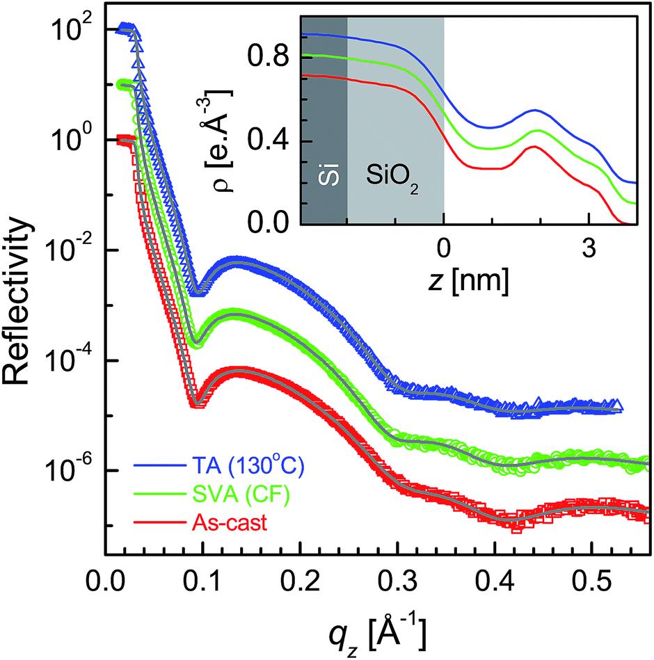 | ||
| Fig. 1 XR data and analyzed curves for a as-cast SL-CF–P3DDT/OH–Si film and after SVA and TA treatments. Inset: corresponding analyzed EDPs. XR curves and EDPs are shifted vertically for clarity. | ||
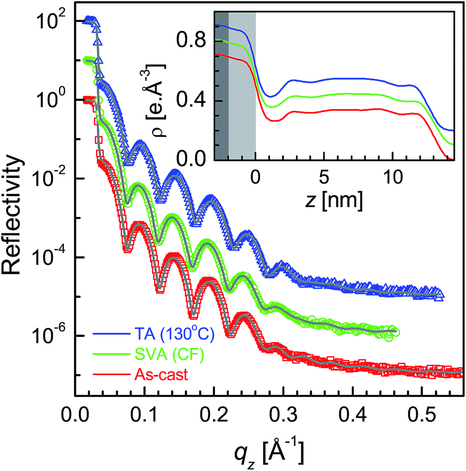 | ||
| Fig. 2 XR data and analyzed curves for a as-cast ML-CF–P3DDT/OH–Si film and after SVA and TA treatments. Inset: corresponding analyzed EDPs. XR curves and EDPs are shifted vertically for clarity. | ||
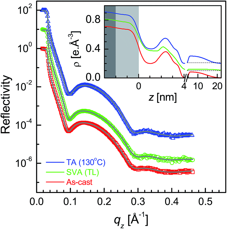 | ||
| Fig. 3 XR data and analyzed curves for a as-cast SL-TL–P3DDT/OH–Si film and after SVA and TA treatments. Inset: corresponding analyzed EDPs. XR curves and EDPs are shifted vertically for clarity. | ||
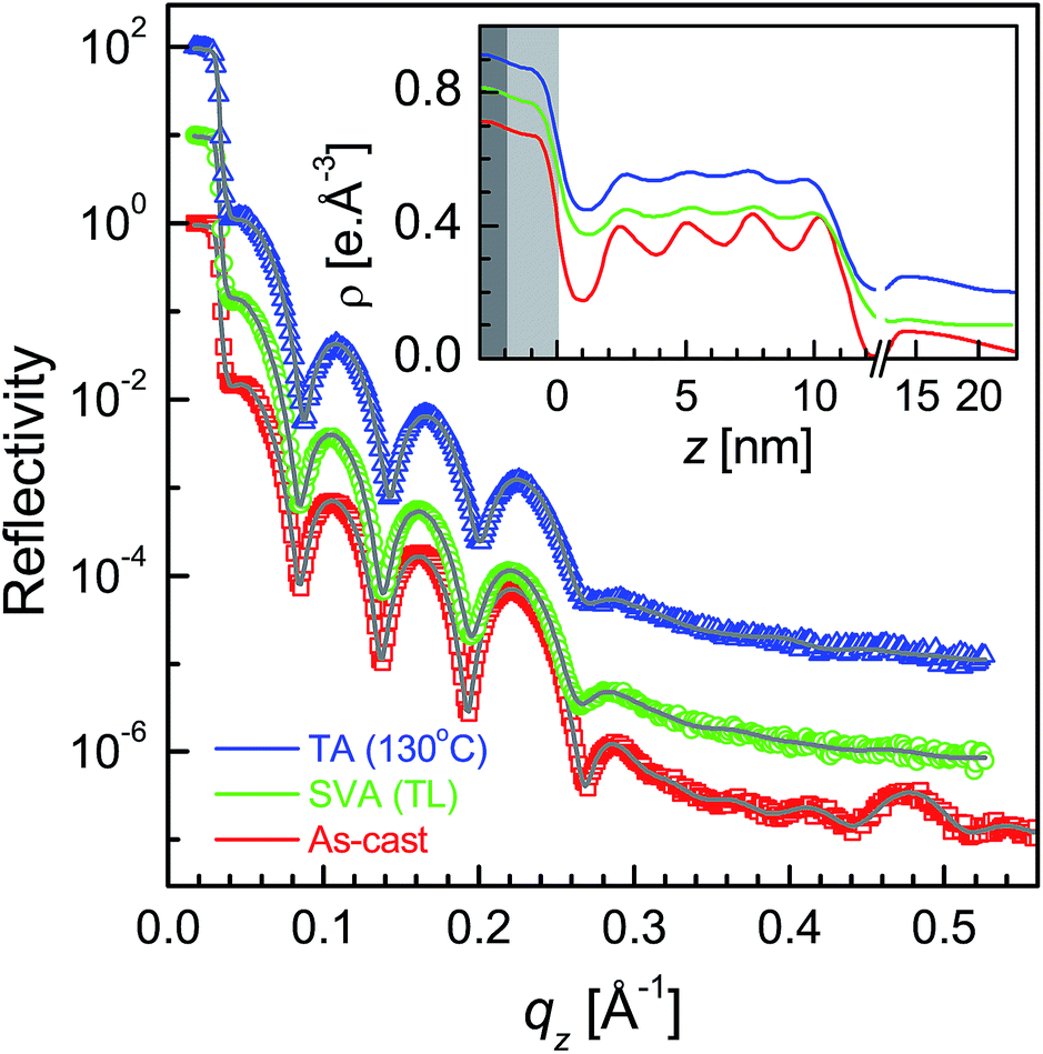 | ||
| Fig. 4 XR data and analyzed curves for a as-cast ML-TL–P3DDT/OH–Si film and after SVA and TA treatments. Inset: corresponding analyzed EDPs. XR curves and EDPs are shifted vertically for clarity. | ||
To get the quantitative information about the films and their small change after SVA and TA, all XR profiles have been analyzed using Parratt's formalism51 after incorporating roughness at each interface.15 It is necessary to mention that the simple 1-layer or 2-layer model, which mainly arises due to the amorphous structure of the film without or with low density interfacial layer, cannot fit the XR data (as shown in Fig. S1–S4 of the ESI†). Rather 3-layer (of low-high-low density due to predominantly edge-on structure) or m-layer (i.e. repetition of 3-layer structure) models are essential for the analysis (as shown in Fig. S1–S4 of the ESI†). It is clear that the better contrast between low and high density layers and/or their periodicity towards uniform value (of about 2.6 nm) suggest better or more edge-on ordering in the film. The best fit XR profiles along with the corresponding EDPs obtained from the analysis are shown in Fig. 1–4. The position of silicon oxide layer in the EDPs are indicated by the gray color. It can be noted that for the films prepared using TL solvent, a layer of large thickness but low density or coverage, on top of the regular single layer or multilayers, was necessary to improve the quality of the XR data fitting, which may be related to some patches in such films and can be neglected for further analysis. On the other hand, the average film thickness (D), the top surface roughness (σtop), the film-substrate interfacial roughness (σin) and the electron density difference between interfacial dip and next peak (Δρ), which are the important parameters to understand the evolution of the structure and/or ordering of the film, are extracted from the EDPs and tabulated in Table 1 for comparison.
| Sample | Solvent | c [mg ml−1] | Treatment | D [nm] | Δρ [e Å−3] | σin [nm] | σtop [nm] | σAFM [nm] | ξ [nm] | σξ [nm] | σd [nm] |
|---|---|---|---|---|---|---|---|---|---|---|---|
| SL-CF–P3DDT/OH–Si | CF | 2/3 | As-cast | 3.4 | 0.11 | 0.44 | 0.20 | 0.26 | 48 | 17.0 | 30 |
| SVA (CF) | 3.5 | 0.09 | 0.47 | 0.21 | 0.07 | 6 | 2.2 | 5 | |||
| TA (130 °C) | 3.4 | 0.09 | 0.47 | 0.22 | 0.09 | 9 | 2.9 | 8 | |||
| ML-CF–P3DDT/OH–Si | CF | 2 | As-cast | 13.0 | 0.06 | 0.45 | 0.65 | 0.27 | 12 | 3.5 | 6 |
| SVA (CF) | 13.0 | 0.07 | 0.45 | 0.65 | 0.26 | 19 | 5.0 | 8 | |||
| TA (130 °C) | 12.6 | 0.11 | 0.45 | 0.65 | 0.15 | 15 | 4.2 | 7 | |||
| SL-TL–P3DDT/OH–Si | TL | 1 | As-cast | 3.7 | 0.16 | 0.39 | 0.17 | 0.28 | 48 | 14.0 | 30 |
| SVA (TL) | 3.5 | 0.06 | 0.45 | 0.37 | 0.10 | 9 | 2.6 | 8 | |||
| TA (130 °C) | 3.6 | 0.15 | 0.41 | 0.16 | 0.12 | 11 | 3.0 | 8 | |||
| ML-TL–P3DDT/OH–Si | TL | 3 | As-cast | 11.2 | 0.22 | 0.36 | 0.50 | 0.14 | 9 | 2.6 | 5 |
| SVA (TL) | 11.2 | 0.08 | 0.45 | 0.70 | 0.21 | 9 | 2.4 | 5 | |||
| TA (130 °C) | 11.0 | 0.11 | 0.42 | 0.68 | 0.20 | 11 | 2.9 | 6 |
It is clear from the EDPs (Fig. 1) and the parameters (Table 1) that there is very little change in the SL-CF–P3DDT/OH–Si film after SVA and TA. Moderate value of Δρ in the as-cast film suggests moderate edge-on oriented ordering of P3DDT in near single layer, the value of which decreases, while the value of both the roughness (σin and σtop) increases slightly after annealing suggesting slight deterioration in the edge-on ordering. For the as-cast ML-CF–P3DDT/OH–Si film the value of Δρ is found very low, suggesting very little edge-on oriented ordering of P3DDT near the substrate and in the subsequent layers. After annealing such Δρ-value increases a little but no change occurs in any roughness value, suggesting slight improvement in the edge-on oriented ordering of P3DDT only near the film-substrate interface especially after TA. Thus for the P3DDT films prepared from CF solvent the effect of annealing in the edge-on oriented ordering of P3DDT near the film-substrate interface is found opposite for single- and multi-layer stack films. For the as-cast SL-TL–P3DDT/OH–Si film the value of Δρ is found quite high when compared with the SL-CF–P3DDT/OH–Si film, suggesting better edge-on oriented ordering of P3DDT in the film. After SVA, the roughness value increases and the Δρ-value decreases appreciably suggesting quite strong deterioration in the edge-on oriented ordering of P3DDT. Interestingly after TA, the ordering in the film is nearly recovered. Finally for the as-cast ML-TL–P3DDT/OH–Si film the value of Δρ is found highest and the value of σin is found lowest among all the films, suggesting the best edge-on oriented ordering of P3DDT near the film-substrate interface. Also better ordering is found throughout this film. After SVA, the roughness value increases and the Δρ-value decreases significantly suggesting strong deterioration in the edge-on oriented ordering of P3DDT. After TA, the ordering in the film is recovered but only to some extent. Thus for the P3DDT films prepared from TL solvent the effect of annealing in the edge-on oriented ordering of P3DDT near the film-substrate interface is found qualitatively similar for single- and multi-layer stack films.
3.2 Topography and in-plane structures
Typical AFM images of the four films (as-cast and after SVA and TA) in two different scan ranges are shown in Fig. 5–8. Defects in the topography of the films are obvious from all the images. Such defects are a clear indication that the films are far from being continuous and smooth along in-plane and out-of-plane directions, respectively, and give rise to grain-like film structures with voids and surface roughness. However, the size of the grains, the size and number of the voids and the roughness or height-fluctuation of the surface varies with the film and also with the post annealing conditions.In order to get the proper visualization about the height-fluctuation, bearing ratio (i.e. coverage as a function of height) estimated from the AFM images are presented in Fig. 5–8. The height-fluctuation can be quantified through roughness value (σAFM), which is tabulated in Table 1. Large height-fluctuation in the as-cast SL-CF–P3DDT/OH–Si film (as evident from both Fig. 5 and Table 1) decreases significantly after annealing. For the ML-CF–P3DDT/OH–Si film (see Fig. 6 and Table 1), the large height-fluctuation in the as-cast film remains almost same (though changes slightly in nature) after SVA but decreases appreciably after TA. The height-fluctuation of the SL-TL–P3DDT/OH–Si film is found similar to that of the SL-CF–P3DDT/OH–Si film, that is, large height-fluctuation in the as-cast film decreases significantly after annealing (see Fig. 7 and Table 1). For the ML-TL–P3DDT/OH–Si film (see Fig. 8 and Table 1), the nature is somewhat different. The small height-fluctuation in the as-cast film increases slightly after annealing.
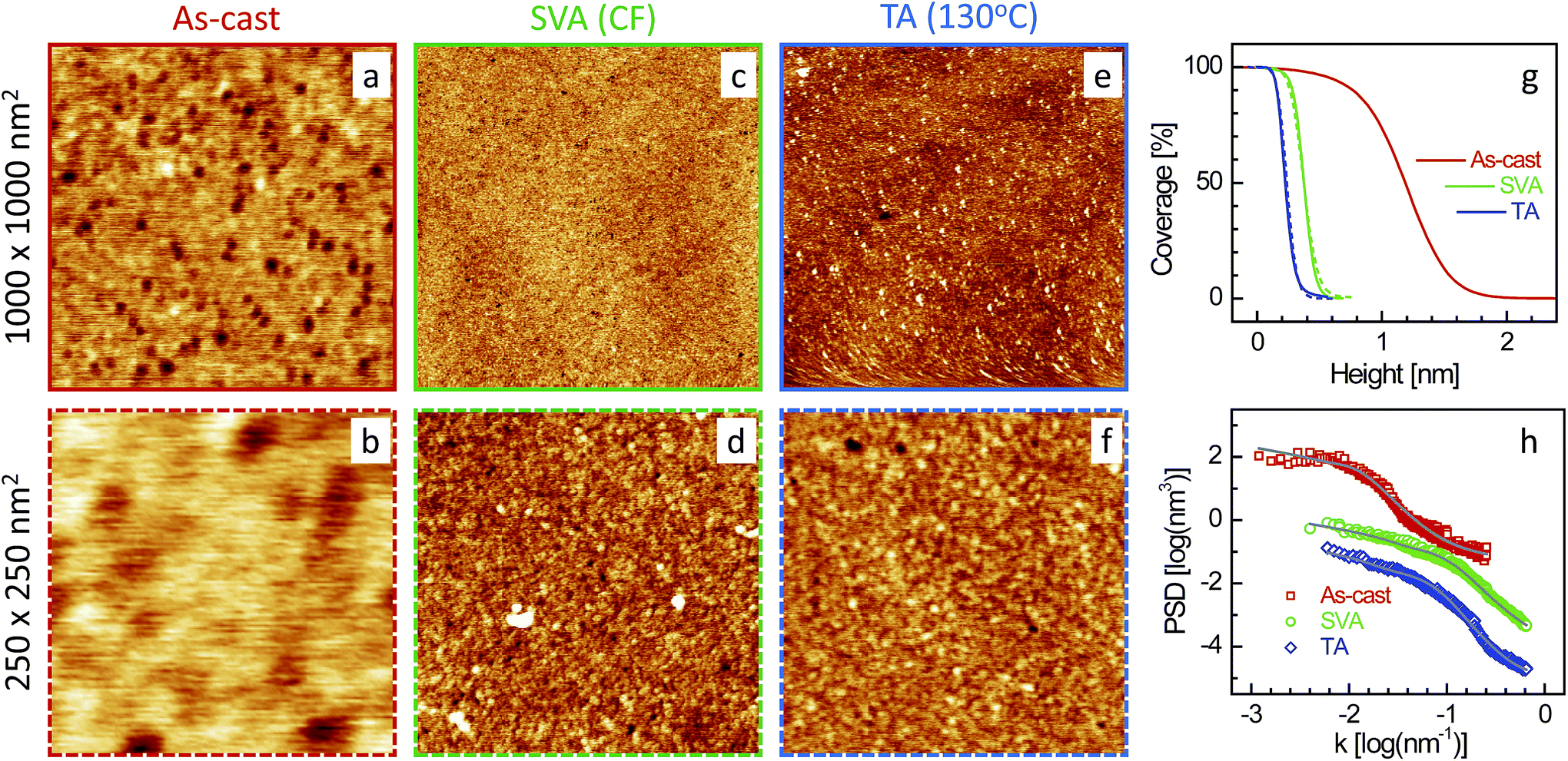 | ||
| Fig. 5 Typical AFM images of a SL-CF–P3DDT/OH–Si film: (a and b) for as-cast, (c and d) after SVA and (e and f) after TA in two different length scales (a, c and e for scan size: 1000 × 1000 nm2 and b, d and f for scan size: 250 × 250 nm2), and corresponding (g) bearing ratio and (h) power spectral density (PSD) profiles (different symbols) and analyzed curves (solid lines). PSD curves are shifted vertically for the clarity. | ||
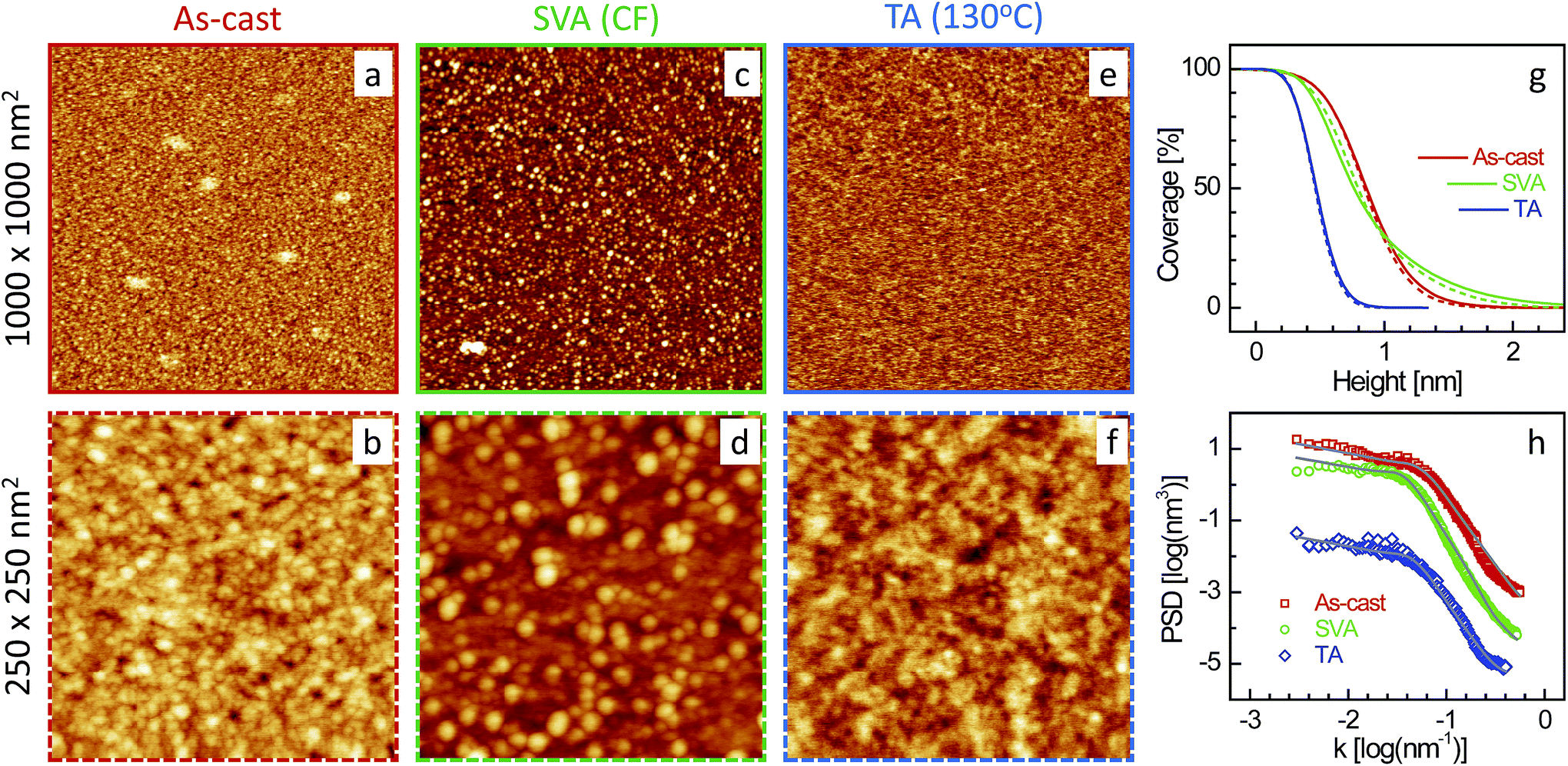 | ||
| Fig. 6 Typical AFM images of a ML-CF–P3DDT/OH–Si film: (a and b) for as-cast, (c and d) after SVA and (e and f) after TA in two different length scales (a, c and e for scan size: 1000 × 1000 nm2 and b, d and f for scan size: 250 × 250 nm2), and corresponding (g) bearing ratio and (h) power spectral density (PSD) profiles (different symbols) and analyzed curves (solid lines). PSD curves are shifted vertically for the clarity. | ||
 | ||
| Fig. 7 Typical AFM images of a SL-TL–P3DDT/OH–Si film: (a and b) for as-cast, (c and d) after SVA and (e and f) after TA in two different length scales (a, c and e for scan size: 1000 × 1000 nm2 and b, d and f for scan size: 250 × 250 nm2), and corresponding (g) bearing ratio and (h) power spectral density (PSD) profiles (different symbols) and analyzed curves (solid lines). PSD curves are shifted vertically for the clarity. | ||
 | ||
| Fig. 8 Typical AFM images of a ML-TL–P3DDT/OH–Si film: (a and b) for as-cast, (c and d) after SVA and (e and f) after TA in two different length scales (a, c and e for scan size: 1000 × 1000 nm2 and b, d and f for scan size: 250 × 250 nm2), and corresponding (g) bearing ratio and (h) power spectral density (PSD) profiles (different symbols) and analyzed curves (solid lines). PSD curves are shifted vertically for the clarity. | ||
Now to have a better idea about the in-plane information or the height–height correlation, the PSD52,53 for all the films, extracted from the AFM images of different scan size,43 are also plotted in Fig. 5–8. It can be noted that the PSD is the angular averaged radial distribution of the Fourier transformed AFM image, which can be expressed as
 | (1) |
 | (2) |
It is very clear from Table 1 that the in-plane correlation length or more specifically the value of ξ of the as-cast SL-CF–P3DDT/OH–Si and SL-TL–P3DDT/OH–Si films are quite large, which decreases considerably after SVA and recovers very little after TA. The decrease in the value of ξ after annealing is the indication of the deterioration in the ordering or crystallinity of the film. However, the decrease in the value of σAFM suggests that there is a strong decrease in the size and depth of the defects as well. Such decrease counterbalances to a large extent the apparent deterioration in the quality of the film. On the other hand, the value of ξ of the as-cast ML-CF–P3DDT/OH–Si and ML-TL–P3DDT/OH–Si films are quite small, which, after annealing, increases a little bit. However, for the ML-TL–P3DDT/OH–Si film, the value of σAFM increases appreciably, which effectively deteriorates the quality of the film, while for the ML-CF–P3DDT/OH–Si film, the roughness value decreases with the small increase in grain-size, which essentially suggests that annealing only improves the quality of this film.
3.3 Overall structures and effect of annealing
Now by combining the information obtained from XR and AFM techniques one can easily visualize the overall structures of the spin-coated P3DDT/OH–Si films. It is clear that as-cast SL-CF–P3DDT/OH–Si and SL-TL–P3DDT/OH–Si films are composed of relatively large-size grains with predominantly edge-on orientated ordered monolayer structures and large size defects. After annealing, although there is an appreciable reduction in the size of the defects, there is a large decrease in the size of the grains as well. The latter essentially increases the grain boundary region, which dominates over defects and effectively the edge-on ordering remains almost same or deteriorates a little bit and so the quality of the film. On the other hand, as-cast ML-CF–P3DDT/OH–Si and ML-TL–P3DDT/OH–Si films are composed of relatively small-size grains. The ordering of the edge-on oriented multilayer grains is weak for the first one, while relatively strong for the second one. After annealing, the size of such small grains remains almost same or increases little bit and the ordering of the multilayered grains became weak for both the films. As a result, the quality of the annealed ML-CF–P3DDT/OH–Si film improves slightly (due to small increase in the grain size), while that of the annealed ML-TL–P3DDT/OH–Si film deteriorates appreciably (due to strong deterioration in the grain ordering).It is known that the structure of a spin-coated thin film is strongly influenced by the nature of the solvent, the substrate surface and the deposition conditions. The surface free energy, polar–nonpolar (hydrophilic–hydrophobic) or electrostatic nature of a substrate surface are strongly influenced by the surface passivation, which can then control the substrate–polymer interactions.15,16,41,42,47,54,55 For example, the adsorption/interaction of P3DDT molecules on/with the weak-hydrophilic OH–Si substrate has been predicted weak,15 which helps the in-plane diffusion and organization of P3DDT molecules, overcoming the fast evaporation induced immobilization during spin-coating. It can be noted that the spinning of solution during such deposition conditions forces the polymer backbones to lie on the surface, which then try to arrange in predominantly edge-on oriented structures. The latter is because the edge-on configuration maximizes the coverage of the low-energy methyl groups at both interfaces and thus it is likely the lowest energy configuration state.56 The arrangement is prominent when monolayer thickness is formed (as evident from the large size predominantly edge-on oriented grains for the as-cast SL films), where interfacial interaction helps the polymer diffusion and ordering. On the other hand, when multilayer thickness is formed through spin coating, the evaporation rate (E) of the solvent becomes important. Fast evaporation of chloroform (E = 11.6)57 creates hindrance in the diffusion and thus in the organization of the P3DDT molecules, particularly above the first layer, which are not in direct contact with the substrate (low contrast between the low and high density layers in the EDP), while the slow evaporation of toluene (E = 2.24)57 allows sufficient time to the P3DDT molecules to diffuse and organize (relatively high contrast between the low and high density layers in the EDP). Accordingly, well ordered edge-on orientated structure is observed in the as-cast ML-TL–P3DDT/OH–Si film. However, the in-plane size or extent of the edge-on orientated grains decreases considerably for the multilayer films. This is probably due to out-of-plane interaction between P3DDT molecules, which creates hindrance in the extent of the in-plane ordering and thus in the grain-size.
The SVA of the films is carried out, by placing the as-cast films and a small beaker containing the solvent inside a covered container, i.e., at saturated vapor pressure for 2 h and then removing the cover. The saturated vapor is likely to increase the mobility of the polymer to a great extent, which is likely to destroy all the ordering. Evaporation of solvent after removal of the cover is unable to recover all the ordering. This is particularly noticeable for the monolayer thick films, where the large-size grains formed during spin-coating technique (due to laying of polymer backbones on the substrate and weak substrate–polymer interaction) are dewetted after SVA to form much small size grains. Further TA can not improve the deteriorated ordering to a large extent as it can not fully recover the size of the grains. For the multilayer films, where the grain-size of the as-cast film is small, it is well recovered after SVA, suggesting that normal evaporation of solvent after large mobility of the polymer during SVA, can form such small size grains. However, the grain–grain ordering is deteriorated which is particularly evident for the ML-TL–P3DDT/OH–Si film, where the ordering of the as-cast film was high. Further TA, although recovers some ordering through diffusion, the recovery is very small.
The observed decrease in the size of defects after annealing, which is expected to improve the electrical transport properties of the film, will certainly be nullified by the deterioration in the ordering of the film during annealing. The latter is due to the uncontrolled diffusion of polymers, particularly for the SVA, where a large intake of good solvent under saturated vapor pressure essentially tries to dissolve the polymer i.e. it dislodges/destroys the existing π–π stacking of the polymer and subsequently their rod-like conformation (to coil-like). Subsequent uncontrolled fast evaporation of the good solvent neither helps to improve nor even helps to recover the unfavorable23 rod-like conformation (from coil-like) of the polymer and their π–π stacking. As a result, small size grains and poor ordering are observed after SVA, which is not recovered even after further TA. Thus it suggests that the controlled annealing of the film is necessary for the relaxation of stress, the annihilation of defects (created during spin-coating) and the organization of molecules to obtain P3DDT films with better order and less defects for the improved device properties.
To verify this we have performed thermal annealing (at 130 °C) in presence of solvent vapor (SVTA) of an as-deposited ML-P3DDT film. The XR data and the analyzed profiles of the as-deposited ML-P3DDT film and after SVTA are shown in Fig. 9. The enhancement of the pseudo Bragg peak (at around qz ≈ 0.24 Å−1) and the appearance of the second order peak after SVTA are clearly evident. This corresponds to the improvement in the edge-on ordering of P3DDTs in the film after SVTA, which is clearly evident from the enhancement in the electron density contrast between high density polymer backbone and low density side chains of P3DDT (see the analyzed EDPs in the inset of Fig. 9). The drastic improvement of the edge-on ordering upon SVTA can be visualized as follows. First the temperature restrict or control the amount of solvent vapor. Such limited vapor pressure in presence of an optimum intermediate temperature [between melting of the alkyl side chains (53 °C) and polythiophene backbones (163 °C)]23 helps the reorganization to form edge-on oriented structure.
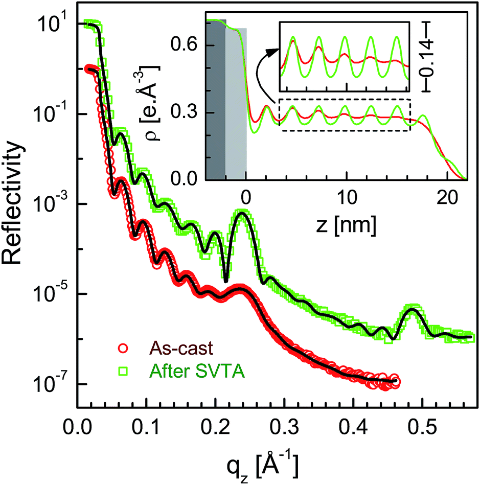 | ||
| Fig. 9 XR data and analyzed curves for a as-cast ML-P3DDT film and after SVTA. XR curves are shifted vertically for clarity. Inset: corresponding analyzed EDPs. A portion of the EDPs is magnified to show the enhancement in the density contrast between high density polymer backbone and low density side chains, due to the improvement in the edge-on ordering after SVTA. | ||
4 Conclusions
The effect of annealing (both SVA and TA) on the structures of the spin-coated monolayer (D ≈ 3.4 nm) and multilayer (D ≈ 11 nm) thin films of P3DDT on OH-terminated Si substrates, prepared using chloroform and toluene solvents, were studied using XR and AFM techniques. The information about the edge-on conformation of the P3DDT molecules and their ordering is obtained from the EDPs, while the information about the in-plane size of the grain-like structures of the films is obtained from the analyzed PSD profiles. The size of the grains (ξ ≈ 50 nm) for the monolayer films is found relatively large compared to that (ξ ≈ 10 nm) of the multilayer films. The weak polymer–substrate and polymer–air interactions are mainly responsible for the edge-on oriented large-size grains in the monolayer films, while solvent evaporation rate also plays an important role for the multilayer films, where the interaction between out-of-plane P3DDT molecules exist. Accordingly, better ordering is only formed in the multilayer film prepared using toluene solvent (as the evaporation of toluene is much slow compared to the chloroform). SVA of the film decreases the size of the defects created during spin coating. However, SVA also deteriorates the ordering in the films. Considerable intake of a good solvent under saturated vapor pressure is likely to destroy most of the existing lameller structures of the polymer and their conformation. Subsequent uncontrolled fast evaporation of the good solvent and further TA can not recover the unfavorable rod-like conformation of the polymer and their π–π stacking, while thermal annealing in presence of solvent vapor can significantly enhance the edge-on ordering of multilayer thin films which is of utmost necessity to obtain improved device properties.References
- G. Yu, J. Gao, J. C. Hummelen, F. Wudi and A. J. Heeger, Science, 1995, 270, 1789–1791 CAS.
- Y. Liang, Z. Xu, J. Xia, S.-T. Tsai, Y. Wu, G. Li, C. Ray and L. Yu, Adv. Mater., 2009, 21, 1349–1353 CrossRef.
- G. Li, R. Zhu and Y. Yang, Nat. Photonics, 2012, 6, 153–161 CrossRef CAS.
- J. H. Burroughes, D. D. C. Bradley, A. R. Brown, R. N. Marks, K. Mackay, R. H. Friend, P. L. Burns and A. B. Holmes, Nature, 1990, 347, 539–541 CrossRef CAS.
- M. Berggren, O. Inganas, G. Gustafsson, J. Rasmusson, M. R. Andersson, T. Hjertberg and O. Wennerstrom, Nature, 1994, 372, 444–446 CrossRef CAS.
- L. Qiu, W. H. Lee, X. Wang, J. S. Kim, J. A. Lim, D. Kwak, S. Lee and K. Cho, Adv. Mater., 2009, 21, 1349–1353 CrossRef CAS.
- H. Yan, Z. Chen, Y. Zheng, C. Newman, J. R. Quinn, F. Dotz, M. Kastler and A. Facchetti, Nature, 2009, 457, 679–686 CrossRef CAS PubMed.
- K.-Y. Jen, G. G. Miller and R. L. Elsenbaumer, J. Chem. Soc., Chem. Commun., 1986, 17, 1346–1347 RSC.
- R. Elsenbaumer, K. Jen and R. Oboodi, Synth. Met., 1986, 15, 169–174 CrossRef CAS.
- H. Sirringhaus, P. J. Brown, R. H. Friend, M. M. Nielsen, K. Bechgaard, B. M. W. Langeveld-Voss, A. J. H. Spiering, R. A. J. Janssen, E. W. Meijer, P. Herwig and D. M. de Leeuw, Nature, 1999, 401, 685–688 CrossRef CAS.
- R. J. Kline, M. D. McGehee, E. N. Kadnikova, J. Liu and J. M. J. Frechet, Adv. Mater., 2003, 15, 1519–1522 CrossRef CAS.
- V. Causin, C. Marega, A. Marigo, L. Valentini and J. M. Kenny, Macromolecules, 2005, 38, 409–415 CrossRef CAS.
- A. Babel and S. A. Jenekhe, Synth. Met., 2005, 148, 169–173 CrossRef CAS.
- J.-F. Chang, B. Sun, D. W. Breiby, M. M. Nielsen, T. I. Solling, M. Giles, I. McCulloch and H. Sirringhaus, Chem. Mater., 2004, 16, 4772–4776 CrossRef CAS.
- I. Roy and S. Hazra, Soft Matter, 2015, 11, 3724–3732 RSC.
- R. J. Kline, M. D. McGehee and M. F. Toney, Nat. Mater., 2006, 5, 222–228 CrossRef.
- M. Brinkmann and J.-C. Wittmann, Adv. Mater., 2006, 18, 860–863 CrossRef CAS.
- H. Yang, S. W. LeFevre, C. Y. Ryu and Z. Bao, Appl. Phys. Lett., 2007, 90, 172116 CrossRef.
- A. Salleo, R. J. Kline, D. M. DeLongchamp and M. L. Chabinyc, Adv. Mater., 2010, 22, 3812–3838 CrossRef CAS PubMed.
- S. T. Shabi, S. Grigorian, M. Brinkmann, U. Pietsch, N. Koenen, N. Kayunkid and U. Scherf, J. Appl. Polym. Sci., 2012, 125, 2335–2341 CrossRef.
- M. A. Ruderer, S. M. Prams, M. Rawolle, Q. Zhong, J. Perlich, S. V. Roth and P. Müller-Buschbaum, J. Phys. Chem. B, 2010, 114, 15451–15458 CrossRef CAS PubMed.
- J.-N. Tisserant, G. Wicht, O. F. Gobel, E. Bocek, G.-L. Bona, T. Geiger, R. Hany, R. Mezzenga, S. Partel, P. Schmid, W. B. Schweizer and J. Heier, ACS Nano, 2013, 7, 5506–5513 CrossRef CAS PubMed.
- I. Roy and S. Hazra, RSC Adv., 2015, 5, 665–675 RSC.
- J. Ficker, A. Ullmann, W. Fix, H. Rost and W. Clemens, J. Appl. Phys., 2003, 94, 2638–2641 CrossRef CAS.
- J. Jaczewska, I. Raptis, A. Budkowski, D. Goustouridis, J. Raczkowska, M. Sanopoulou, E. Pamula, A. Bernasik and J. Rysz, Synth. Met., 2007, 157, 726–732 CrossRef CAS.
- K. Yoshino, Y. Manda, K. Sawada, M. Onoda and R. Sugimoto, Solid State Commun., 1989, 69, 143–146 CrossRef CAS.
- Y. Ohmori, M. Uchida, K. Muro and K. Yoshino, Solid State Commun., 1991, 80, 605–608 CrossRef.
- S.-A. Chen and J.-M. Ni, Macromolecules, 1992, 25, 6081–6089 CrossRef CAS.
- K. C. Park and K. Levon, Macromolecules, 1997, 30, 3175–3183 CrossRef CAS.
- I. F. Perepichka, D. F. Perepichka, H. Meng and F. Wudl, Adv. Mater., 2005, 17, 2281–2305 CrossRef CAS.
- W. Xu, L. Li, H. Tang, H. Li, X. Zhao and X. Yang, J. Phys. Chem. B, 2011, 115, 6412–6420 CrossRef CAS PubMed.
- Y. Guo, Y. Jin and Z. Su, Soft Matter, 2012, 8, 2907–2914 RSC.
- B. A. Gregg, J. Phys. Chem., 1996, 100, 852–859 CrossRef CAS.
- A. A. Rudov, E. S. Patyukova, I. V. Neratova, P. G. Khalatur, D. Posselt, C. M. Papadakis and I. I. Potemkin, Macromolecules, 2013, 46, 5786–5795 CrossRef CAS.
- T. Kim, J. Hwang, W. Hwang, J. Huh, H.-C. Kim, S. Kim, J. Hong, E. Thomas and C. Park, Adv. Mater., 2008, 20, 522–527 CrossRef CAS.
- E. J. W. Crossland, K. Rahimi, G. Reiter, U. Steiner and S. Ludwigs, Adv. Funct. Mater., 2011, 21, 518–524 CrossRef CAS.
- G. Lu, L. Li and X. Yang, Adv. Mater., 2007, 19, 3594–3598 CrossRef CAS.
- I. K. Robinson and D. J. Tweet, Rep. Prog. Phys., 1992, 55, 599–651 CrossRef CAS.
- X-Ray and Neutron Reflectivity: Principles and Applications, ed. J. Daillant and A. Gibaud, Springer, Paris, 1999 Search PubMed.
- J. K. Bal and S. Hazra, Phys. Rev. B: Condens. Matter Mater. Phys., 2009, 79, 155405 CrossRef.
- J. K. Bal and S. Hazra, Phys. Rev. B: Condens. Matter Mater. Phys., 2007, 75, 205411 CrossRef.
- J. K. Bal and S. Hazra, Phys. Rev. B: Condens. Matter Mater. Phys., 2009, 79, 155412 CrossRef.
- M. Mukhopadhyay and S. Hazra, RSC Adv., 2016, 6, 12326–12336 RSC.
- W. Kern, J. Electrochem. Soc., 1990, 137, 1887–1892 CrossRef CAS.
- H. F. Okorn-Schmidt, IBM J. Res. Dev., 1999, 43, 351–365 CrossRef CAS.
- X. G. Zhang, Electrochemistry of Silicon and its Oxide, Kluwer Academic, New York, 2004 Search PubMed.
- P. Chatterjee, S. Hazra and H. Amenitsch, Soft Matter, 2012, 8, 2956–2964 RSC.
- S. Hazra, Appl. Surf. Sci., 2006, 253, 2154–2157 CrossRef CAS.
- P. Chatterjee and S. Hazra, J. Phys. Chem. C, 2014, 118, 11350–11356 CAS.
- I. Horcas, R. Fernández, J. M. Gómez-Rodriguez, J. Colchero, J. Gómez-Herrero and A. M. Baro, Rev. Sci. Instrum., 2007, 78, 013705 CrossRef CAS PubMed.
- L. G. Parratt, Phys. Rev., 1954, 95, 359–369 CrossRef.
- J. M. Elson and J. M. Bennett, Appl. Opt., 1995, 34, 201–208 CrossRef CAS PubMed.
- S. J. Fang, S. Haplepete, W. Chen, C. R. Helms and H. Edwards, J. Appl. Phys., 1997, 82, 5891–5898 CrossRef CAS.
- B. Meredig, A. Salleo and R. Gee, ACS Nano, 2009, 3, 2881–2886 CrossRef CAS PubMed.
- J. K. Bal, S. Kundu and S. Hazra, Phys. Rev. B: Condens. Matter Mater. Phys., 2010, 81, 045404 CrossRef.
- H. Hlaing, X. Lu, T. Hofmann, K. Yager, C. Black and B. Ocko, ACS Nano, 2011, 5, 7532–7538 CrossRef CAS PubMed.
- Safety Data Sheet, LabChem, http://www.labchem.com.
Footnote |
| † Electronic supplementary information (ESI) available. See DOI: 10.1039/c6ra25560d |
| This journal is © The Royal Society of Chemistry 2017 |