DOI:
10.1039/C6RA26178G
(Paper)
RSC Adv., 2017,
7, 1110-1117
Fluorinated benzothiadiazole and indacenodithieno[3,2-b]thiophene based regioregular-conjugated copolymers for ambipolar organic field-effect transistors and inverters†
Received
2nd November 2016
, Accepted 25th November 2016
First published on 4th January 2017
Abstract
We report the synthesis and characterization of a series of three soluble polymeric hybrids in benzothiadiazole–indacenodithieno[3,2-b]thiophene based ladder-type polymers (BT–IDTT) containing the acceptor unit 3,6-dithien-2-yl-2,5-dialkylpyrrolo[3,4-c]pyrrole-1,4-dione (DTDPP), and donor moieties 7,8-bithienyl benzo[1,2-b:4,5-b′]di-thiophene (BDTT) and 4,8-bis(5-ethylhexylselenophen-2-yl)benzo[1,2-b:4,5-b′]dithiophene (BDTSe) in BT–IDTT–DTDPP (P1), BT–IDTT–BDTT (P2) and BT–IDTT–BDTSe (P3) copolymers to tune the strength of ambipolar charge-carrier transport properties for organic field-effect transistors (OFETs) and ambipolar complementary inverters. A narrow band gap of 1.4–1.7 eV was achieved by the careful selection of the electron donor–acceptor unit and strong packing of those polymers in the film state. In particular, a very narrow bandgap of 1.38 eV and well-balanced ambipolar transistor characteristics were achieved by replacing benzodithiophene in P2 and P3 with diketopyrrolopyrrole in P1. Optimized top gate bottom contact OFETs with P1 polymer showed electron and hole mobilities of 0.015 and 0.007 cm2 V−1 s−1 respectively, and inverter gain of ∼14 using poly(methyl methacrylate) gate dielectric. Interestingly, hole transport properties were improved to a mobility of 0.1 cm2 V−1 s−1 in all OFETs with the BT–IDTT ladder-type polymer using fluorinated P(VDF-TrFE) dielectric, which can be ascribed to the increased hole accumulation at the semiconductor–dielectric interface.
Introduction
Conjugated polymers have been extensively researched due to their excellent opto-electrical and electrical properties for a wide range of applications such as organic light emitting diodes (OLEDs), organic field-effect transistors (OFETs), organic photovoltaics (OPVs), and organic sensors.1–4 In the design of conjugated polymers, diverse principles and strategies are employed to tune their opto-electrical properties for the specific requirements. Hence, studies on structure and property relationships have been important research areas in organic electronics. One recent focus is alternating donor (D) and acceptor (A) moieties in conjugated polymers with various building blocks. Combination of various electron D–A units in one copolymers provides the highest occupied molecular orbital (HOMO) and lowest unoccupied molecular orbital (LUMO) energy levels; controls the energy band gap, extends intramolecular charge delocalization, leading to broadened absorption wavelength and improved power conversion efficiency in organic photovoltaic cells (OPVs), charge carrier mobility in OFETs, and tuning emission color in OLEDs.5–7 Side chains, such as alkyl or aryl groups also contribute significantly to processability in solution state and intermolecular interactions between monomers to improve solubility and ordering of conjugated polymers for better charge carrier transport.8,9
Considering the charge-carrier transport properties of this class of polymers, hole-transport behavior has been observed in almost all D–A conjugated polymers. Robust n-type (electron transport) or ambipolar behavior has been reported to depend on the type of acceptor moieties used.10 Recent progress in D–A polymers as active layers for OFETs has yielded materials with mobilities consistently exceeding 0.1 cm2 V−1 s−1 and some exceeding 10 cm2 V−1 s−1.11 Among numerous building block for conjugated polymers, indacenodithieno[3,2-b]thiophene (IDTT), a mutifused ladder-type donor moiety, has performed exceptionally well in polymeric semiconductors due to its longer effective conjugation and better planarity, enhancing electron delocalization along the polymer backbone and producing high hole mobility.12 In addition, 4,8-bis(5-(2-ethylhexyl)thiophen-2-yl)benzo[1,2-b:4,5-b′]dithiophene (BDTT) has been widely employed as electron donor unit for OPV applications due to their relatively large and planar conjugated structure which is favorable for π–π stacking, improving carrier transport and absorption in long wavelengths compared to 4,8-bis(2-ethylhexyloxy)benzo[1,2-b:4,5-b′]dithiophene.13 Similarly, 4,8-bis(5-(2-ethylhexyl)selenophene-2-yl)benzo[1,2-b:4,5-b′]dithiophene (BDTSe) and 3,6-dithien-2-yl-2,5-dialkylpyrrolo[3,4-c]pyrrole-1,4-dione (DTDPP) have also been developed, and have broader absorption and balanced HOMO and LUMO energy levels, providing high performance in OPVs.14,15 The electron deficient lactam rings in DTDPP produce acceptor moiety with strong electron withdrawing effect and enhanced π–π interaction.16
In this study, we focus on molecular structure property relationships, combining DTDPP, BDTT and BDTSe D–A building blocks to tune electron and hole mobilities in polymer OFETs. By replacing the electron rich BDT unit in BT–IDTT–BDTT (P2) and BT–IDTT–BDTSe (P3) polymer with diketopyrrolopyrrole (DPP) in BT–IDTT–DTDPP (P1) (Scheme 1), a very narrow bandgap of 1.38 eV and well-balanced ambipolar transistor characteristics are achieved. The well-balanced ambipolar charge transport was observed in these polymers with DTDPP based polymers, showing electron and hole mobilities of 0.015 and 0.007 cm2 V−1 s−1 respectively, and the highest inverter gain of ∼14 with poly(methyl methacrylate) (PMMA) dielectric. Hole mobility was further improved using high-k fluorinated P(VDF-TrFE) dielectric to ∼0.1 cm2 V−1 s−1 for all the BT–IDTT ladder-type based polymer OFETs.
 |
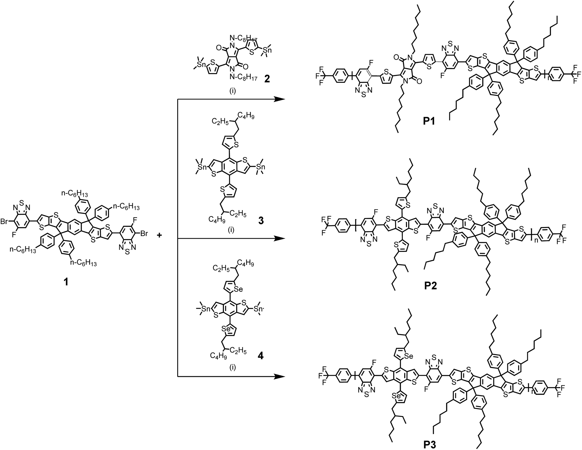
| | Scheme 1 Synthetic route for P1, P2, and P3. Reagents and conditions: (i) Pd2(dba)3, P(o-tol)3, chlorobenzene, heating was accomplished using a microwave reactor. | |
Experimental section
Synthesis and characterization
To begin, the 3,6-dibromo-5-fluoro-IDTT (monomer 1) was prepared by the Stille-coupling reaction as shown in ESI (Scheme S1†).17 DTDPP (monomer 2), BDTT (monomer 3), and BDTSe (monomer 4) were purchased from commercial sources. Using these monomers, three conjugated copolymers with regioregular orientations in the polymer backbone were synthesized using microwave assisted Stille cross coupling polymerization reaction, as shown in Scheme 1 and purified by sequential Soxhlet extraction with methanol, hexane, dichloromethane, chloroform, and chlorobenzene, and then the chlorobenzene fractions were recovered. Due to the linear alkyl chain, the yield of P1 was relatively lower than those of P2 and P3 polymer with branched alkyl chains. After Soxhlet extraction with chlorobenzene, only P1 polymer remained. However, all polymers from the chlorobenzene fraction had relatively good solubility in common organic solvents, such as chlorobenzene and o-dichlorobenzene. The number-average molecular weights (Mn) and polydispersity indices (PDI, Mw/Mn) of P1, P2, and P3 were determined by GPC at 80 °C in chlorobenzene as an eluent relative to polystyrene standards, as 47![[thin space (1/6-em)]](https://www.rsc.org/images/entities/char_2009.gif) 900; 57900; and 83300 g mol−1 with PDI = 1.26, 1.17, and 1.03, respectively. Differential scanning calorimetry (DSC) for P1, P2, and P3 showed absent endothermic and exothermic peaks over 35–350 °C, indicating a stable film morphology over a wide temperature range (Fig. S2†).
900; 57900; and 83300 g mol−1 with PDI = 1.26, 1.17, and 1.03, respectively. Differential scanning calorimetry (DSC) for P1, P2, and P3 showed absent endothermic and exothermic peaks over 35–350 °C, indicating a stable film morphology over a wide temperature range (Fig. S2†).
Polymerization for P1. Compounds 1 (0.3 g, 0.20 mmol), 2 (0.14 g, 0.20 mmol), tris(dibenzylideneacetone)dipalladium(0) (2 mol%), tri(o-tolyl)phosphine (8 mol%), and 18 mL degassed chlorobenzene were mixed in a 20 mL microwave vial. The mixture was heated at 120 °C for 10 min, 150 °C for 20 min, 170 °C for 30 min, and 180 °C for 10 min in a microwave reactor. After polymerization, the polymer was end capped with 2,5-bis(trimethylstannyl)thiophene and 4-bromobenzotrifluoride at 150 °C for 30 min each. The polymer was purified by Soxhlet extraction with washing solvent sequence of methanol, hexane, dichloromethane, chloroform, and chlorobenzene. The compound extracted in chlorobenzene was precipitated with methanol, filtered and dried. Yield = 20%, Mn = 47.9 kDa, PDI = 1.26.
Polymerization for P2. Compounds 1 (0.45 g, 0.30 mmol), 3 (0.27 g, 0.30 mmol), tris(dibenzylideneacetone)dipalladium(0) (2 mol%), tri(o-tolyl)phosphine (8 mol%), and 12 mL degassed chlorobenzene were mixed in a 20 mL microwave vial. The mixture was heated at 120 °C for 10 min, 150 °C for 20 min, 170 °C for 30 min, and 180 °C for 10 min in a microwave reactor. After polymerization, the polymer was end capped with 2,5-bis(trimethylstannyl)thiophene and 4-bromobenzotrifluoride at 150 °C for 30 min each. The polymer was purified by Soxhlet extraction with washing solvent sequence of methanol, hexane, dichloromethane, chloroform, and chlorobenzene. The compound extracted in chlorobenzene was precipitated with methanol, filtered and dried. Yield = 52%, Mn = 57.9 kDa, PDI = 1.17.
Polymerization for P3. Compounds 1 (0.31 g, 0.21 mmol), 4 (0.21 g, 0.21 mmol), tris(dibenzylideneacetone)dipalladium(0) (2 mol%), tri(o-tolyl)phosphine (8 mol%), and 12 mL degassed chlorobenzene were mixed in a 20 mL microwave vial. The mixture was heated at 120 °C for 10 min, 150 °C for 20 min, 170 °C for 30 min, and 180 °C for 10 min in a microwave reactor. After polymerization, the polymer was end capped with 2,5-bis(trimethylstannyl)thiophene and 4-bromobenzotrifluoride at 150 °C for 30 min each. The polymer was purified by Soxhlet extraction with washing solvent sequence of methanol, hexane, dichloromethane, chloroform, and chlorobenzene. The compound extracted in chlorobenzene was precipitated with methanol, filtered and dried. Yield = 50%, Mn = 83.8 kDa, PDI = 1.03.
OFET fabrication
Top gate bottom contact geometry was used for all devices. Using conventional photolithography method, source and drain contact electrodes (13/3 nm = Au/Ni) were patterned on glass substrates by thermal evaporation deposition. The channel length and channel width are 10 μm and 1000 μm respectively. The glass substrates were then cleaned using deionized water, acetone, and isopropanol for 10 min each in a sonication bath. BT–IDTT polymer solutions in 5 mg mL−1 chlorobenzene (Sigma Aldrich) were spin coated at 2000 rpm for 60 s, and then thermally annealed at 150 °C for 30 min. After cooling, PMMA (Sigma Aldrich, Mn = 120 kDa, 80 mg mL−1 in n-butyl acetate) or P(VDF-TrFE) (Solvay, 70:30 mol% random copolymer, 30 mg mL−1 in methyl ethyl ketone) layer was deposited on the BT–IDTT polymer film by spin coating at 2000 rpm for 60 s, followed by annealing at 80 °C for 2 h in a nitrogen purged glove box to remove residual solvent. Completion of OFET devices was achieved by depositing 50 nm Al as gate electrode via thermal evaporation using a shadow mask. Electrical characteristics of the BT–IDTT devices were measured using a Keithley 4200 parameter analyzer on a probe station in a nitrogen filled glove box.
Complementary inverters fabrication. The source and drain contacts (Au/Ni) of the inverters were patterned by photolithography, as above. Following the same transistor fabrication detailed above, P1, P2 and P3 polymers and PMMA as gate dielectric layers were spun, and thermal annealed. The top-gated inverters were completed by the depositing Al gate electrodes (50 nm thick) by evaporation on the active regions of the transistors using a metal shadow mask.
Thin film and characterization
The electrical characteristics of the BT–IDTT polymer OFETs and complementary inverters were measured using a Keithley 4200 parameter analyzer on a probe station in a nitrogen filled glove box. Optical spectra were measured by UV-vis absorption spectroscopy. The surface microstructures were examined using non-contact mode atomic force microscopy (Nanoscope, Veeco Instruments, Inc.).
Results and discussion
Optical and electrochemical properties
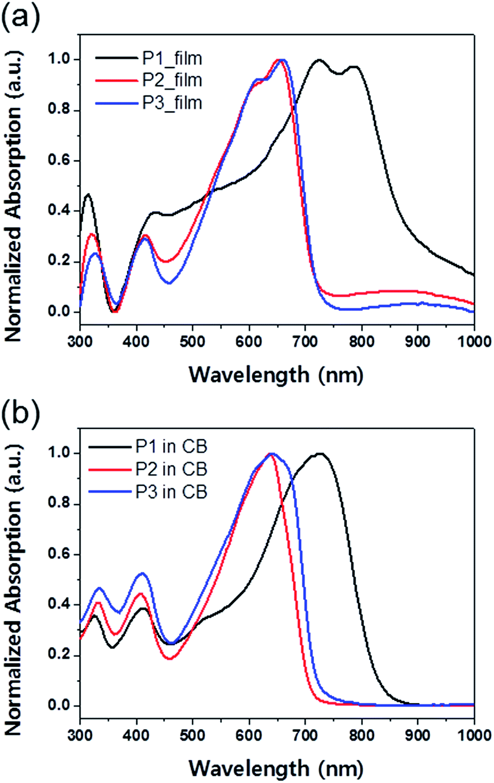
The normalized UV-vis absorption spectra of copolymers P1, P2, and P3 in chlorobenzene solution and as thin films are presented in Fig. 1, and the corresponding optoelectronic properties, including the absorption peak wavelengths, absorption edge wavelengths, and optical band gaps, are summarized in Table 1. Unlike P2 and P3 copolymers, based on BDTT and BDTSe, respectively, P1 exhibited a broad absorption band from 300–850 nm due to inclusion of DTDPP.18 Due to the selenophene side chain, P3 showed absorption red-shifted approximately 5–10 nm in solution and film compared with P2.19 All the copolymers in film demonstrated distinct vibrational features next to their absorption maxima, indicating the existence of ordered aggregation and strong intermolecular π–π stacking. The optical band gaps (Eoptg) of the polymer thin films were determined from their onset of the absorption edges as 1.38, 1.72, and 1.72 eV for P1, P2, and P3 respectively.
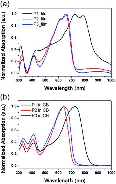 |
| | Fig. 1 UV-vis absorption spectra of BT–IDTT based polymers (a) as thin films and (b) in chlorobenzene solution. | |
Table 1 Molecular weights, optical and electrochemical properties of the BT–IDTT based polymers
| Polymer |
Mn (kDa)/PDIa |
λsolutionmax (nm) |
λsolutionedge (nm) |
λfilmmax (nm) |
λfilmedge (nm) |
Eoptgb (eV) |
EHOMOc (eV) |
ELUMOc (eV) |
Eelecg c (eV) |
| Number-average molecular weight (Mn) and PDI of the polymers were determined by GPC at 80 °C in chlorobenzene as an eluent. Optical band gap was determined from onset of the absorption in film. The HOMO, LUMO and electrochemical band gap were estimated from cyclic voltammetry measurement. |
| P1 |
48.0/1.26 |
410.4, 723.5 |
823.6 |
314.6, 724.6, 783.3 |
898.9 |
1.38 |
−5.13 |
−3.84 |
1.29 |
| P2 |
57.9/1.17 |
406.1, 634.1 |
707.9 |
321.8, 650.7, 415.7 |
718.5 |
1.72 |
−5.28 |
−3.74 |
1.54 |
| P3 |
83.8/1.03 |
409.2, 641.8 |
719.2 |
657.2, 414.2, 326.4 |
719.2 |
1.72 |
−5.25 |
−3.75 |
1.50 |
The highest occupied molecular orbital (HOMO, EHOMO) and lowest unoccupied molecular orbital (LUMO, ELUMO) were evaluated by cyclic voltammetry (CV) (Fig. S3†), performed with 0.1 M tetrabutylammonium tetrafluoroborate (Bu4NBF4) as the supporting electrolyte at scan rate 100 mV s−1. To estimate the energy levels of both polymers from the vacuum energy level, we used the ferrocene/ferrocenium (Fc/Fc+) redox couple as a calibration reference. The half-wave potential for oxidation of the Fc/Fc+ redox couple is −4.8 eV, below the vacuum level. P2 and P3 showed similar voltammograms, suggesting that the effect of the side chain was negligible. HOMO and LUMO energy level values of the polymers are −5.13 and −3.84, −5.28 and −3.74, and −5.25 and −3.75 eV for P1, P2, and P3 respectively, as summarized in Table 1. As expected from the introduction of the electron withdrawing unit DTDPP, electrochemical band gap (Eelecg = |HOMO − LUMO|) of P1 (1.29 eV) was lower than those of P2 (1.54 eV) and P3 (1.50 eV).
Thin film microstructure analyses
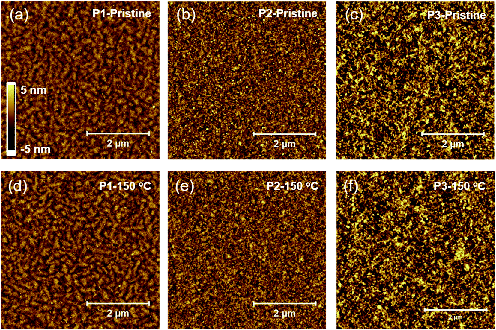
We investigated the surface and bulk microstructure of the BT–IDTT based polymer thin films using atomic force microscopy (AFM) and X-ray diffraction (XRD) analyses. P1 polymer thin films showed nano fibril-like microstructures (Fig. 2a and d) whereas P2 (Fig. 2b and e) and P3 (Fig. 2c and f) films showed similar disordered surface morphology before and after 150 °C annealing, as shown in Fig. 2. XRD analysis showed amorphous film surfaces for both annealed and un-annealed films, with no diffraction peaks (Fig. S4†), which is consistent with other reported IDTT based polymers.20
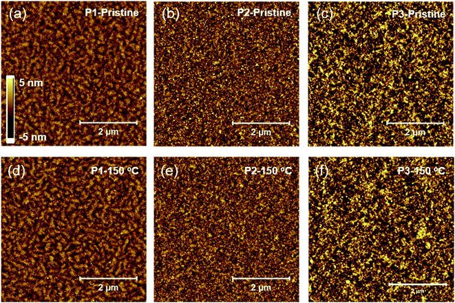 |
| | Fig. 2 Atomic force microscopy height images of pristine and 150 °C annealed P1 (a and d), P2 (b and e), and P3 (c and f) polymers respectively. | |
OFET performance
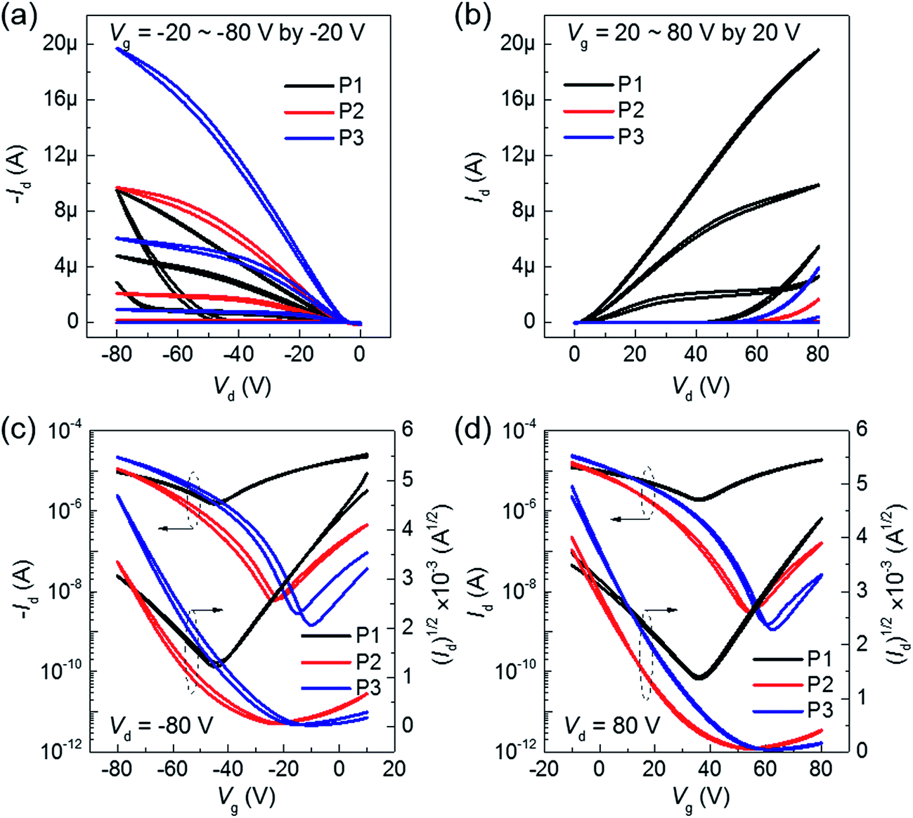
Fig. 3 shows the electrical characteristics of BT–IDTT based OFETs fabricated with top gate bottom contact (TG/BC) geometry and PMMA gate dielectric. As expected, annealed P2 and P3 polymers showed hole dominant p-channel characteristics, with hole mobilities (threshold voltage, VT) of 0.0290 ± 0.0042 cm2 V−1 s−1 (−33.45 ± 1.79 V) and 0.0283 ± 0.0058 cm2 V−1 s−1 (−37.54 ± 3.33 V) respectively, because of the large portion of electron donation units in their backbones. On the other hand, P1 OFETs exhibited well balanced ambipolar charge transfer with hole and electron mobilities 0.0072 ± 0.0013 cm2 V−1 s−1 and 0.0152 ± 0.0026 cm2 V−1 s−1 respectively. Transfer characteristics of un-annealed P1, P2 and P3 OFETs are shown in Fig. S5.† Although DPP acceptor derived polymers have been reported to show insignificant electron transport characteristics with a very low on-current in n-channel operation,21 the stable ambipolar behavior in P1 OFETs was a consequence of the poly(methyl methacrylate) (PMMA) gate dielectric, which is a hydroxyl group-free polymer with few electron trapping groups and very low band gap (∼1.3 eV) facilitating both hole and electron injection.11,22,23 Comparatively, the displayed ambipolarity behavior in P1 OFETs is due to the relatively low-lying HOMO (−5.13) and deep-lying LUMO energy (−3.84 eV) of P1 polymer among three polymers, which facilitated the most favorable hole and electron injection from the Au electrode owing to its low injection barrier. On the other hand, P2 and P3 polymers with deep-lying HOMO energy levels of −5.28 and −5.25 eV respectively showed hole-dominant p-channel OFET behavior with low off-current levels. We therefore hypothesized that the low injection barrier with respect to Au electrode (−5.1 eV) among the polymers does not significantly influence the hole transport properties, but however contributed greatly by the unique polymer facets. As observed in the AFM images (Fig. 2) noticeable difference in the surface microstructures is observed when DTDPP, BDTT and BDTSe are tailored in the BT–IDTT based polymers.
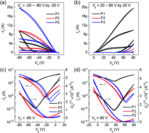 |
| | Fig. 3 Output and transfer characteristics of 150 °C annealed BT–IDTT OFETs with PMMA as gate dielectric in (a), (c) p-channel, and (b), (d) n-channel. | |
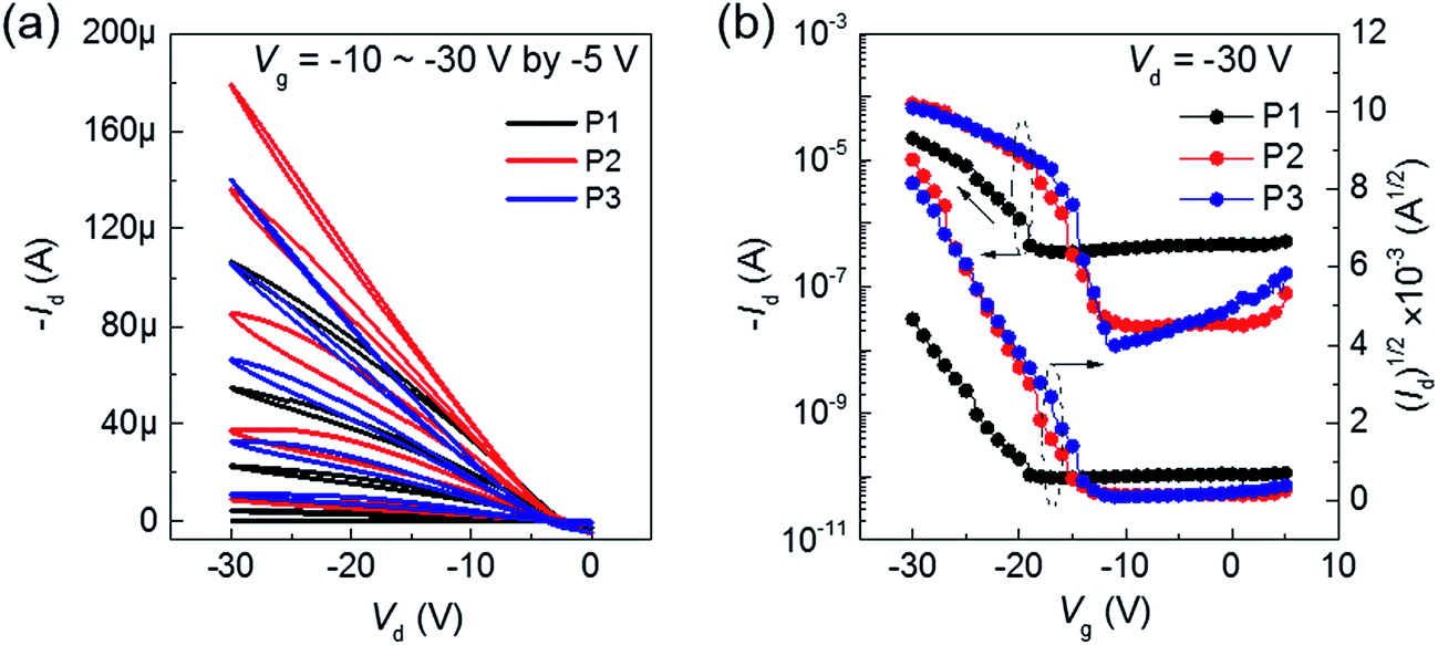
To check the effect of gate dielectric on ambipolar transport, we employed high-k ferroelectric polymer, P(VDF-TrFE) (ε ≈ 10.4), as gate dielectric for the BT–IDTT based OFETs. As shown in Fig. 4, a reduced operating voltage (−30 V) with perfect hole transport characteristics is observed. Improved hole mobility in the order ∼0.1 cm2 V−1 s−1 is achieved in all the BT–IDTT based polymers OFETs, which is owed to the molecular orbital energy modulation through dipoles of P(VDF-TrFE) and BT–IDTT polymer, which pull-up HOMO and LUMO levels of the semiconductor.6,10,12,24 This effect increased accumulated holes at the semiconductor/dielectric interface, while the –C–F dipoles destructively induced depletion or trapping of electrons in the n-transport channel, thereby decreasing the concentration of electrons in the channel, and leading to perfect p-transport characteristics of low operation voltage and the noticeable shift in VT displayed in the BT–IDTT devices with P(VDF-TrFE) dielectric (Fig. 4b).6,13,14,24 Electrical parameters, such mobility (μ), threshold voltage (VT), and current on/off ratio (Ion/off) of BT–IDTT based OFETs are summarized in Table 2.
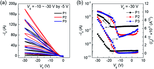 |
| | Fig. 4 (a) Output and (b) transfer characteristics of BT–IDTT–OFETs with P(VDF-TrFE) as gate dielectric. | |
Table 2 Electrical parameters of BT–IDTT OFETs with PMMA and P(VDF-TrFE) dielectrics annealed at 150 °C and as spun
| Polymer |
Dielectric |
T (°C) |
μhole (cm2 V−1 s−1) |
Vth (V) |
Ion/off |
μelec (cm2 V−1 s−1) |
Vth (V) |
Ion/off |
| P1 |
PMMA |
Pristine |
0.0068(±0.0003) |
−11.22(±3.47) |
1.15 ± 0.23 × 101 |
0.0130(±0.0011) |
30.00(±0.89) |
9.95 ± 1.11 |
| PMMA |
150 |
0.0072(±0.0013) |
−16.18(±3.45) |
5.26 ± 0.65 |
0.0152(±0.0026) |
19.71(±3.83) |
8.24 ± 0.89 |
| P(VDF-TrFE) |
150 |
0.094 (±0.016) |
−19.62(±1.59) |
4.35 ± 1.73 × 101 |
N.A |
| P2 |
PMMA |
Pristine |
0.0227(±0.0029) |
−46.34(±1.67) |
1.64 ± 0.62 × 10³ |
0.0005(±0.0002) |
48.22(±5.26) |
1.28 ± 0.31 × 101 |
| PMMA |
150 |
0.0290(±0.0042) |
−33.45(±1.79) |
2.43 ± 1.35 × 10³ |
0.0010(±0.0004) |
61.10(±1.24) |
3.57 ± 1.60 × 101 |
| P(VDF-TrFE) |
150 |
0.109(±0.011) |
−10.28(±1.03) |
2.23 ± 1.22 × 10³ |
N.A |
| P3 |
PMMA |
Pristine |
0.0300(±0.0054) |
−34.31(±0.75) |
3.58 ± 0.18 × 10³ |
0.0006(±0.0001) |
54.15(±2.62) |
2.49 ± 0.32 × 101 |
| PMMA |
150 |
0.0283(±0.0058) |
−37.54(±3.33) |
1.65 ± 0.25 × 10⁴ |
0.0004(±0.0002) |
62.08(±1.34) |
1.85 ± 0.56 × 101 |
| P(VDF-TrFE) |
150 |
0.113(±0.020) |
−13.34(±0.88) |
5.58 ± 1.67 × 10³ |
N.A |
Inverter performance
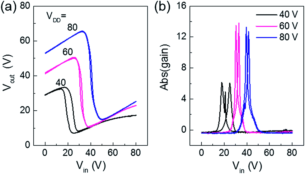
We employed the ambipolar transistor for complementary inverters using a simple blanket coating without patterning the n and p type semiconducting layers. The main advantage of ambipolar complementary circuits is realizing large area integrated circuits by very simple printing processes without complexing patterning process of semiconducting layer.25 P1 OFETs exhibited good symmetric voltage transfer characteristics (Fig. 5a), with negligible hysteresis and high voltage gain (Fig. 5b) of ∼14, using device dimensions Wp/Lp = Wn/Ln = 1 mm/20 μm with PMMA gate dielectrics. On the contrary, P2 and P3 based inverters showed relatively lower gains, ∼5 and ∼2 respectively, with large hysteresis for the same device dimensions (Fig. S6†), which we attribute to unbalanced hole and electron carriers, as verified in the OFETs characteristics. Thus, well balanced ambipolar transport is essential to realize high performance ambipolar complementary circuits.
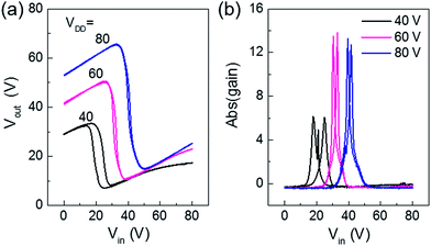 |
| | Fig. 5 (a) Voltage transfer characteristics and (b) corresponding voltage gains at various VDD from 40–80 V of the complementary inverter circuits based on P1 polymers. | |
Conclusions
In conclusion, we investigated the structure property relationships of a newly synthesized series of D–A polymeric hybrids in benzothiadiazole–indacenodithieno[3,2-b]thiophene based ladder-type polymers (BT–IDTT) containing DTDPP acceptor moiety, and BDTT and BDTSe donor units, with the aim of tuning D–A strength of ambipolar charge carrier transport properties for OFET and inverter applications. Optical absorption and electrochemical potential were measured to determine intrinsic optophysical properties and energetic levels. P2 and P3 polymers exhibited comparable absorption spectra and HOMO/LUMO energy levels, whereas a significant red-shift and stepwise decrease and increase in LUMO and HOMO levels, respectively, were observed in the P1 polymer. P1 OFETs exhibited close electron and hole mobilities of 0.015 and 0.007 cm2 V−1 s−1 respectively, and absolute gain of ∼14 in ambipolar inverters due to the PMMA dielectric, relatively lower band-gap (∼1.3 eV) and energy levels. Improved hole mobility of the order of 0.1 cm2 V−1 s−1 is achieved in all BT–IDTT ladder-type based polymers OFETs using fluorinated P(VDF-TrFE) dielectric due to increased hole accumulation at the semiconductor–dielectric interface.
Acknowledgements
This work was supported by the Center for Advanced Soft-Electronics (2013M3A6A5073183) funded by the Ministry of Science, ICT & Future Planning and the LG Research Fund.
Notes and references
- K.-J. Baeg, M. Caironi and Y.-Y. Noh, Adv. Mater., 2013, 25, 4210–4244 CrossRef CAS PubMed.
- N. Chakravarthi, K. Gunasekar, W. Cho, D. X. Long, Y.-H. Kim, C. E. Song, J.-C. Lee, A. Facchetti, M. Song, Y.-Y. Noh and S.-H. Jin, Energy Environ. Sci., 2016, 9, 2595–2602 CAS.
- P. Lin and F. Yan, Adv. Mater., 2012, 24, 34–51 CrossRef CAS PubMed.
- D. Khim, G.-S. Ryu, W.-T. Park, H. Kim, M. Lee and Y.-Y. Noh, Adv. Mater., 2016, 28, 2752–2759 CrossRef CAS PubMed.
- H.-H. Chou and C.-H. Cheng, Adv. Mater., 2010, 22, 2468–2471 CrossRef CAS PubMed.
- G. Kim, S.-J. Kang, G. K. Dutta, Y.-K. Han, T. J. Shin, Y.-Y. Noh and C. Yang, J. Am. Chem. Soc., 2014, 136, 9477–9483 CrossRef CAS PubMed.
- K. Gunasekar, W. Cho, D. X. Long, S. S. Reddy, M. Song, Y.-Y. Noh and S.-H. Jin, Adv. Electron. Mater., 2016, 1600086 CrossRef.
- X. Guo, M. Baumgarten and K. Müllen, Prog. Polym. Sci., 2013, 38, 1832–1908 CrossRef CAS.
- J. Mei and Z. Bao, Chem. Mater., 2014, 26, 604–615 CrossRef CAS.
-
(a) J. A. Letizia, M. R. Salata, C. M. Tribout, A. Facchetti, M. A. Ratner and T. J. Marks, J. Am. Chem. Soc., 2008, 130, 9679–9694 CrossRef CAS PubMed;
(b) R. Mondal, N. Miyaki, H. Becerril, J. E. Norton, J. Parmer, A. C. Mayer, M. L. Tang, J.-L. Bredas, M. McGehee and Z. Bao, Chem. Mater., 2009, 21, 3618–3628 CrossRef CAS.
-
(a) H. Yan, Z. Chen, Y. Zheng, C. Newman, J. R. Quinn, F. Dotz, M. Kastler and A. Facchetti, Nature, 2009, 457, 679–686 CrossRef CAS PubMed;
(b) W. Zhang, J. Smith, S. E. Watkins, R. Gysel, M. McGehee, A. Salleo, J. Kirkpatrick, S. Ashraf, T. Anthopoulos, M. Heeney and I. McCulloch, J. Am. Chem. Soc., 2010, 132, 11437–11439 CrossRef CAS PubMed;
(c) H. N. Tsao, D. M. Cho, I. Park, M. R. Hansen, A. Mavrinskiy, D. Y. Yoon, R. Graf, W. Pisula, H. W. Spiess and K. Müllen, J. Am. Chem. Soc., 2011, 133, 2605–2612 CrossRef CAS PubMed;
(d) H. Bronstein, Z. Chen, R. S. Ashraf, W. Zhang, J. Du, J. R. Durrant, P. S. Tuladhar, K. Song, S. E. Watkins, Y. Geerts, M. M. Wienk, R. A. J. Janssen, T. Anthopoulos, H. Sirringhaus, M. Heeney and I. McCulloch, J. Am. Chem. Soc., 2011, 133, 3272–3275 CrossRef CAS PubMed;
(e) Y. Li, P. Sonar, S. P. Singh, M. S. Soh, M. van Meurs and J. Tan, J. Am. Chem. Soc., 2011, 133, 2198–2204 CrossRef CAS PubMed.
- J. J. Intemann, K. Yao, Y.-X. Li, H.-L. Yip, Y.-X. Xu, P.-W. Liang, C.-C. Chueh, F.-Z. Ding, X. Yang, X. Li, Y. Chen and A. K.-Y. Jen, Adv. Funct. Mater., 2014, 24, 1465–1473 CrossRef CAS.
- L. Ye, S. Zhang, W. Zhao, H. Yao and J. Hou, Chem. Mater., 2014, 26, 3603–3605 CrossRef CAS.
- N. Chakravarthi, K. Kranthiraja, M. Song, K. Gunasekar, P. Jeong, S.-J. Moon, W. S. Shin, I.-N. Kang, J. W. Lee and S.-H. Jin, Sol. Energy Mater. Sol. Cells, 2014, 122, 136–145 CrossRef CAS.
- G. Zhang, Y. Fu, Z. Xie and Q. Zhang, Sol. Energy Mater. Sol. Cells, 2011, 95, 1168–1173 CrossRef CAS.
- J. C. Bijleveld, V. S. Gevaerts, D. D. Nuzzo, M. Turbiez, S. G. J. Mathijssen, D. M. de Leeuw, M. M. Wienk and R. A. J. Janssen, Adv. Mater., 2010, 22, E242–E246 CrossRef CAS PubMed.
- T. Qin, W. Zajaczkowski, W. Pisula, M. Baumgarten, M. Chen, M. Gao, G. Wilson, C. D. Easton, K. Müllen and S. E. Watkins, J. Am. Chem. Soc., 2014, 136, 6049–6055 CrossRef CAS PubMed.
- B. Lim, J.-S. Yeo, D. Khim and D.-Y. Kim, Macromol. Rapid Commun., 2011, 32, 1551–1556 CrossRef CAS PubMed.
- R. Kroon, A. Melianas, W. Zhuang, J. Bergqvist, A. D. de Z. Mendaza, T. T. Steckler, L. Yu, S. J. Bradley, C. Musumeci, D. Gedefaw, T. Nann, A. Amassian, C. Müller, O. Inganäs and M. R. Andersson, Polym. Chem., 2015, 6, 7402–7409 RSC.
- W. Lee, H. Cha, Y. J. Kim, J.-E. Jeong, S. Hwang, C. E. Park and H. Y. Woo, ACS Appl. Mater. Interfaces, 2014, 6, 20510–20518 CAS.
-
(a) Q. T. Zhang and J. M. Tour, J. Am. Chem. Soc., 1997, 119, 5065–5066 CrossRef CAS;
(b) Q. T. Zhang and J. M. Tour, J. Am. Chem. Soc., 1998, 120, 5355–5362 CrossRef CAS;
(c) S. A. Jenekhe, L. Lu and M. M. Alam, Macromolecules, 2001, 34, 7315–7324 CrossRef CAS.
-
(a) H. Usta, A. Facchetti and T. Marks, J. Am. Chem. Soc., 2008, 130, 8580–8581 CrossRef CAS PubMed;
(b) J. Liu, R. Zhang, I. Osaka, S. Mishra, A. E. Javier, D.-M. Smilgies, T. Kowalewski and R. D. McCullough, Adv. Funct. Mater., 2009, 19, 3427–3434 CrossRef CAS;
(c) D. H. Kim, B.-L. Lee, H. Moon, H. M. Kang, E. J. Jeong, J. Park, K.-M. Han, S. Lee, B. W. Yoo, B. W. Koo, J. Y. Kim, W. H. Lee, K. Cho, H. A. Becerril and Z. Bao, J. Am. Chem. Soc., 2009, 131, 6124–6132 CrossRef CAS PubMed;
(d) X. Guo, F. S. Kim, S. A. Jenekhe and M. D. Watson, J. Am. Chem. Soc., 2009, 131, 7206–7207 CrossRef CAS PubMed;
(e) X. Guo, R. P. Ortiz, Y. Zheng, Y. Hu, Y.-Y. Noh, K.-J. Baeg, A. Facchetti and T. J. Marks, J. Am. Chem. Soc., 2011, 133, 1405–1418 CrossRef CAS PubMed.
- Y. He, W. Hong and Y. Li, J. Mater. Chem. C, 2014, 2, 8651–8661 RSC.
- B. Nketia-Yawson, H.-S. Lee, D. Seo, Y. Yoon, W.-T. Park, K. Kwak, H. J. Son, B. Kim and Y.-Y. Noh, Adv. Mater., 2015, 27, 3045–3052 CrossRef CAS PubMed.
- W.-J. Lee, W.-T. Park, S. Park, S. Sung, Y.-Y. Noh and M.-H. Yoon, Adv. Mater., 2015, 27, 5043–5048 CrossRef CAS PubMed.
Footnotes |
| † Electronic supplementary information (ESI) available: Synthesis procedure, cyclic voltammograms and DSC curves for P1, P2 and P3 polymers, X-ray diffraction spectra, additional OFET and inverter characteristics. See DOI: 10.1039/c6ra26178g |
| ‡ These authors contributed equally. |
|
| This journal is © The Royal Society of Chemistry 2017 |
Click here to see how this site uses Cookies. View our privacy policy here. 
 Open Access Article
 This Open Access Article is licensed under a
  *a
*a