 Open Access Article
Creative Commons Attribution 3.0 Unported Licence
Roll-to-roll slot die production of 300 mm large area silver nanowire mesh films for flexible transparent electrodes†
Byung-Yong Wanga,
Eung-Seok Leeb,
Dae-Soon Limb,
Hyun Wook Kang *c and
Young-Jei Oh*de
aCenter for Semiconductor Technology, Korea University, 145 Anam-ro, Seongbuk-gu, Seoul, 02841, Republic of Korea
bDepartment of Materials Science and Engineering, Korea University, 145 Anam-ro, Seongbuk-gu, Seoul, 02841, Republic of Korea
cDepartment of Mechanical Engineering, Chonnam National University, 77 Yongbong-ro, Buk-gu, Gwangju 61186, Republic of Korea. E-mail: kanghw@chonnam.ac.kr; Tel: +82-62-530-1662
dOpto Electronic Materials and Devices Center, Korea Institute of Science and Technology, 5 Hwarang-ro 14-gil, Seongbuk-gu, Seoul 02792, Republic of Korea. E-mail: youngjei@kist.re.kr; Tel: +82-2-958-5553
eDepartment of Nano Materials Science and Engineering, University of Science and Technology, 217 Gajeong-ro, Yuseong-gu, Daejeon 34113, Republic of Korea
First published on 23rd January 2017
Abstract
To develop flexible transparent electrodes, an ink fabricated with silver nanowires (AgNWs) was coated on a polyethylene terephthalate substrate using a roll-to-roll slot die machine. The AgNW used in the manufacturing of the transparent electrode is a highly transparent conductive material that is very close to commercialization due to its low sheet resistance, low heat treatment temperature, and high transmittance. An AgNW ink was optimized for the slot die process, which was prepared using the optimized formulation with AgNWs, solvent, and dispersant. As a result, high-quality transparent conductive films were successfully manufactured with 32–94 Ω sq−1 of sheet resistance, 1.3–3.2 of haze and 86.2–92% transmittance with a width of 300 mm. To verify the possibilities in optoelectronic applications, organic solar cells were fabricated with the AgNW mesh transparent electrode and showed a good performance of 7.65% efficiency, which was better than the result obtained using an indium tin oxide-based electrode.
1. Introduction
Transparent sheet conducting electrodes are applied to various devices such as displays, solar cells, and touch panels. Indium tin oxide (ITO) has been most frequently used as a transparent electrode due to its excellent electrical and optical properties, such as high electrical conductivity, superior chemical stability, and high light transmittance. However, because ITO is formed by a physical vapor deposition (PVD) method, such as sputtering and e-beam evaporation, it has drawbacks such as the high cost of electrode film formation, difficulties of achieving flexibility, and fabrication on a plastic substrate or film.1–9For this reason, several studies have been conducted on using a printed electronics technique with metal paste or silver nanowires for the formation of transparent electrodes. The technique of printed electronics allows large area fabrication through a relatively simple process with the advantages of low process temperatures, low cost, and eco-friendliness.10,11 Moreover, the printed electronics technique can be easily used to make devices on a flexible substrate, which is difficult to implement in conventional manufacturing processes. With these points of view, printed electronics can be used to fabricate flexible electronic devices and parts, including solar cells, displays, RFID (radio frequency identification), thin film transistors, and printed circuit boards (PCBs).12,13
The printed electronics technique is largely classified into contact and non-contact printing techniques. The contact printing technique includes gravure, gravure off-set, flexo, reverse off-set, roll-to-plate printing, and screen printing. Most contact printing methods, which transfer ink to a blanket roll and then to a substrate, are appropriate for the formation of micro-patterns, but they give a relatively low resolution, high influence of ink, and thin printing thickness. Thus, they are suitable for forming printed circuits.14–17 On the otherhand, the non-contact printing technique, which include slot-die, ink-jet, and spray, have been designed to pattern or coat functional materials onto a target substrate without any contact between the substrate and printing device. Due to the distinguishing advantages of contact printing, such as its wide selectivity of printing materials, large printable area, and maskless patterning, this technology is widely applied in various industrial fields.17
The slot-die method, which is most frequently used for the formation of transparent electrodes, causes no damage to the substrate through contact when the conductive material is coated on a substrate and is optimized for the fast production of thin precise coating products. The slot-die coating injects ink into the slot-die using a gear pump and discharges a certain amount of ink. The discharged ink from the slot-die is coated on the substrate and forms a thin film. The desired thickness of the thin film is governed by the volume flow rate of ink, the physical properties of the ink (viscosity, surface tension etc.), the thickness of the shim plate inside the slot-die, and the feed speed of the film. Furthermore, as the ink used for coating is stored inside a sealed container, it does not show problems such as changing viscosity and contamination by foreign substances. Moreover, slot-die coating has an easy configuration and simple process steps that present low manufacturing costs and mass production conditions. Therefore, the slot-die coating technique has been widely used in numerous application fields and is mainly used in the manufacture of flexible transparent electrodes.18–20
Because the slot-die method is sensitive to the feed speed of the substrate film, thickness of the substrate film, ink flow rate, coating gap, shim plate thickness, the contact angle when the coating fluid contacts the web, and the physical properties of the web, they must be investigated in advance. Moreover, the ink properties are appropriately adjusted to avoid instabilities, such as leakage, bead break-up, and ribbing problems during the die coating process. Moreover, metal nanowire-based ink was used in this study; the solvent type, the size and shape of the nanowires, and the degree of dispersion of the ink were carefully decided to perform a successful manufacturing process.21 In addition, non-uniformity of the film thickness that affects the quality of the final device needs to be avoided. To keep the coating process stable, the process conditions, such as the physical properties of the coating fluid, the die structure, and operation conditions, were analyzed and maintained.
2. Experimental
2.1 Preparation of silver nanowire (AgNW) ink
AgNWs were fabricated via the polyol method.22 To manufacture AgNW ink, the polyvinylpyrrolidone (PVP) used for the AgNWs fabrication must be removed because it decreases the electrical conductivity at the connection point between the AgNWs. In addition, abnormally grown AgNWs and Ag nanoparticles during the AgNWs synthesis were eliminated because they have a negative effect on the electrical conductivity and haze. Finally, the AgNWs need to be purified. Through six or more washing cycles using DI water and acetone, the PVP is completely removed. Then, the AgNWs solution was purified via centrifugation at 2000 rpm for 10 min. After that, the precipitate was discarded and the supernatant was retained. As a result, AgNWs with an average diameter of 40 nm and a length of 40 μm were obtained. To produce the AgNW ink suitable for the slot die coating process, 1.2 wt% of the aforementioned AgNWs were dispersed in a mixed solution. The solution consists of ethylene glycol (2 vol%) in isopropyl alcohol (98 vol%), which is frequently used for printed electronics ink. This adjusts the evaporation temperature of the solvent upon drying. Agglomeration of the AgNWs was avoided using 0.005 g mL−1 of polymer dispersant (D520 Nafion dispersion – alcohol-based 100 EW, Dupont) to the final ink. The dispersion stability of the manufactured ink was verified for 24 hours using a Turbiscan system. In addition, the wettability of the surface when the AgNW ink was deposited on a substrate film was tested using a contact angle analyzer (BS150, Surface. Tech).2.2 Manufacturing the transparent conductive film
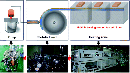
An R2R slot die machine was used to fabricate the transparent conductive film using the AgNW ink. A 100 μm-thick PET film (NPLUS Co., Ltd.) was used as the substrate. On the PET film, 5 μm coating of acrylic resin was used as an over-coating layer with 90% transmittance. More detailed specifications of the substrate are listed in Table 1. If the contact angle is high enough because the surface energy is too small during coating process, the coated droplets agglomerate, which makes it difficult to form a normal transparent conductive film. In order to form a high-quality transparent conductive film, the surface energy on the substrate must be controlled. Therefore, a film with an over-coated acrylic resin (NPLUS Co., Ltd.) was used on the PET substrate. The R2R slot die machine, used for the AgNW ink coating process, consisted of the slot die (coating zone, 30 cm), a roll for ink coating, a controller for adjusting the film feed speed and ink discharge quantity, a pump for ink feeding to the slot die, and heating zones for heat treatment of the coated film (see Fig. 1). The slot die conditions are listed in Table S1.†| Total thickness | 105 μm | |
| PET thickness | 100 μm | |
| Acrylic resin thickness | 5 μm | |
| Visual light transmittance | More than 90% | |
| Haze | Less than 2% | |
| Surface hardness | 3H | |
| Adhesive strength (H/C) | 100/100 (5B) | |
| Heat shrinkage | MD | 1.4% |
| TD | 0.5% | |
2.3 Characterization of the transparent conductive film
The sheet resistance was measured via a 4-point probe method using a Keithley 2400 source meter. The transmittance was analyzed using an ultraviolet-visible spectrometer (Perkin Elmer UV/Vis spectrometer Lamda 18). Due to the light reflection property of the AgNWs, the haze phenomenon reflected on the AgNWs surface was observed using a haze spectrometer (Sinco). The surface morphology was observed using SEM (XL-30 EDAX, Philips, Netherlands), confocal laser scanning microscopy (CLSM, Olympus) and atomic force microscopy (AFM) (Digital Instruments Dimension 3100, equipped with a Nanoscope IV controller). To estimate the flexibility of the transparent conductive film, the mechanical properties of the transparent electrodes based on PET/AgNW and PET/ITO were compared using a bending test (ZB-100, Z-Tech) at a radius of 10 mm for 10![[thin space (1/6-em)]](https://www.rsc.org/images/entities/char_2009.gif) 000 cycles.
000 cycles.
3. Results and discussion
For the preparation of AgNW ink, the removal of PVP from the AgNW surface, which shows a negative effect on the electrical conductivity, is crucial. Fig. 2 shows the SEM images of the AgNW films and conductivity curve as a function of washing count. After the 1st washing cycle, the PVP was not removed from the AgNWs surface, but the AgNWs showed several organic coating layers. Due to this reason, the electrical resistance was not measured. After the 2nd washing cycle, a PVP film still existed inside the AgNWs and the electrical resistance was again, not detected. However, an electrical resistance of 3.4 kΩ appeared after the 3rd washing cycle. This high resistance value was due to the sparse remaining PVP that was not fully removed. Finally, the PVP was completely removed after the 6th washing cycle and the resistance was very low due to the connection between the AgNWs.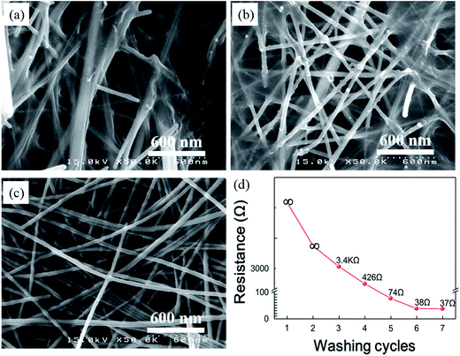 | ||
| Fig. 2 SEM images of the AgNWs according to their washing condition: (a) without washing, (b) washing 3-times and (c) washing 6-times. (d) The resistance changes upon the different washing cycles. | ||
The PVP layer with a thickness of 40 nm or greater was shown on the AgNW surface after the 1st washing cycle; however, the PVP fully disappeared from the AgNWs' surface after the 6th washing cycle (see Fig. S1 in the ESI†). Furthermore, some impurities (e.g. Ag nanoparticles) were generated during the synthesis of the AgNWs and increased the haze when used as a transparent electrode. Particularly, high surface roughness results in difficultly in device fabrication. After purification using centrifugation at 2000 rpm for 10 min, only AgNWs existed with no impurities (see Fig. S2 in the ESI†).
Fig. S3† shows the CLSM images of the transparent conductive film when using a dispersant. The films were prepared by mixing an ethylene glycol solution into isopropyl alcohol, which gave the best characteristics for ink manufacturing, as obtained from our preliminary experiments. If no dispersant is used for ink formation, agglomeration of the AgNWs, which results in a negative effect on the electrical and optical properties, will be observed. The CLSM images show that the AgNWs are agglomerated and the sheet resistance is higher than 138 Ω sq−1 when no polymer dispersant is used. When the polymer dispersant was used, the coating was uniform without agglomeration and the sheet resistance was as low as 28 Ω sq−1 because the electrons could easily move along the network of AgNWs.
Fig. 3a shows the precipitation as a function of the amount of dispersant added to the AgNWs solution in a glass bottle. Due to the van der Waals forces, the AgNWs are agglomerated and settle over time. The AgNW ink was kept at room temperature for seven days after their manufacture and the precipitation phenomenon was observed. When no dispersant was added, all the AgNWs are fully precipitated in the ink. As the amount of dispersant was increased, the height of precipitation was reduced and reached a perfect dispersion state with no precipitation at 0.005 g mL−1. However, when more dispersant (>0.005 g mL−1) was added, the AgNWs precipitated. This is a general phenomenon that appears when the dispersant content is changed. The polymer dispersant generates a great number of polymer chains on the surface of the AgNWs, which are entangled with one another and leads to the agglomeration and precipitation of the AgNWs. However, the precipitation characteristics change even due to very fine vibrations in the dispersion stability assessment of this precipitation. Fig. 3b explains the dispersion stability of the AgNW ink with 0.005 g mL−1 dispersant that showed the best characteristics, which was observed for 24 hours by Turbiscan. Turbiscan measures the light flux (%) of the transmitted and the back-scattered light by scanning the measuring cell, which contains the sample, using near-infrared rays as the light source and thereby checks the dispersion stability from the profile change according to the changing dispersion state of the ink. The experimental results obtained for the dispersion stability of the AgNWs show that the AgNWs did not agglomerate or precipitate even after 24 hours, confirming that the light flux (%) of the transmitted and the back-scattered light does not change.23
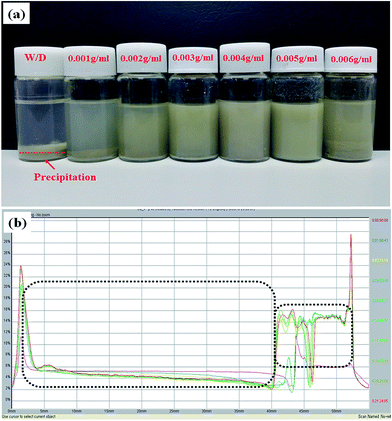 | ||
| Fig. 3 (a) Precipitation as a function of the amount of dispersant added to the AgNWs solution and (b) Turbiscan analysis for the dispersion stability of the AgNWs. | ||
The pseudoplastic behavior of the AgNW ink that passes the slot die during coating, which was checked by viscosity of the ink, is shown in Fig. S4.† The viscous behavior of ink must keep a pseudoplastic behavior in which the viscosity decreases as the shear rate increases. The reason for this is to achieve a flat coating on the substrate by lowering the viscosity of the ink passing through slot die; if the ink viscosity is increased, the ink cannot easily spread on the substrate, resulting in agglomeration and a non-uniform thickness.24–26 The AgNW ink prepared in this study exhibits shear-thinning behavior by which the viscosity decreases as the shear rate increases. In order to form a transparent conductive film with the AgNW ink, the substrate surface must have a good wettability for the AgNW ink. When the wettability was checked according to the substrate type, the PET substrate without an over-coating layer showed wettability with 22.3° contact angle, the glass substrate showed a contact angle of 32.6°, and the PET substrate with over-coated acrylic resin, which was used in this study, showed an excellent wettability with a contact angle of 12.7° (Fig. 4).
 | ||
| Fig. 4 The contact angles of the AgNW ink droplets observed on different substrates: (a) glass, (b) PET and (c) PET/over coated acrylic resin. | ||
As shown in Fig. 5, ink dispersed with 1.2 wt% AgNWs was used to confirm the optimum slot die coating conditions. The gap between the slot die and the substrate was fixed at 0.05 mm and the slot die shim thickness was varied between 30, 50, and 100 μm. The optimum coating conditions were found by controlling the substrate feeding speed and the RPM of the gear pump at each shim thickness. The experimental results showed that as the substrate feeding speed was lower and the RPM was higher, the air hole and dripping phenomena increased due to excessive ink discharge and an overspill phenomenon occurred as the ink overflowed in the opposite direction of the substrate feeding direction instead of being smeared on the substrate. Furthermore, when the substrate feeding speed was fast, a break line was easily formed towards the substrate movement direction due to the fast substrate feeding speed regardless of the ink discharging quantity.
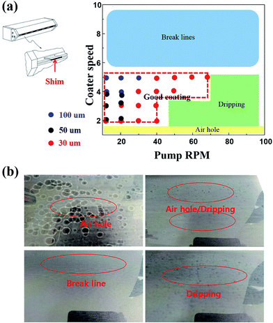 | ||
| Fig. 5 (a) A schematic of the three different shim plate regimes in a “good coating window” plot, (b) photographs of the coating defects: air holes, dripping and break lines. | ||
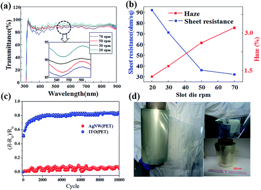
Based on the previous experiment, the best coating characteristics in this study were obtained for the largest area when a shim plate thickness of 30 μm was used. Characteristics of the transparent conductive film were observed according to the gear pump speed (RPM) at the shim plate thickness of 30 μm. As shown in Fig. 6, the AgNWs coverage density increased as the printing speed (RPM) increased. Based on the results obtained for the optical transparency, haze, and sheet resistance, the AgNWs conductive layer thickness and AgNW coverage density were optimized using a printing speed between 30 and 50 RPM. The change in the AgNWs coverage density in the coated transparent conductive film influenced the electrical and optical properties. It was observed that by increasing the AgNWs content, the number of electron movement paths and the haze value were increased, and the sheet resistance of the transparent conductive film and transmittance were decreased (Fig. 7a and b). Based on the above data, various transparent conductive electrodes with a low sheet resistance of 32–94 Ω sq−1, haze of 1.3–3.2 and high transmittance of 86.2–92% were successfully produced in this study. The standard deviation of the haze and sheet resistance are below 10%. Fig. 7c compares the durability between indium tin oxide (ITO) and the AgNW transparent electrodes after bending up to 10![[thin space (1/6-em)]](https://www.rsc.org/images/entities/char_2009.gif) 000 cycles. In the case of the ITO transparent electrode, the ITO film displayed cracks when the inside radius during bending was decreased due to the brittleness of ITO, which results in a rapid resistance change, and the resistance changes were varied by at least 70% when compared to the initial resistance even after 500 cycles. On the other hand, the AgNW transparent electrode maintained a constant resistance value even when the inside radius of bending was decreased, and the resistance change was negligible even after 10
000 cycles. In the case of the ITO transparent electrode, the ITO film displayed cracks when the inside radius during bending was decreased due to the brittleness of ITO, which results in a rapid resistance change, and the resistance changes were varied by at least 70% when compared to the initial resistance even after 500 cycles. On the other hand, the AgNW transparent electrode maintained a constant resistance value even when the inside radius of bending was decreased, and the resistance change was negligible even after 10![[thin space (1/6-em)]](https://www.rsc.org/images/entities/char_2009.gif) 000 cycles, indicating its improved mechanical stability when compared to that of the ITO transparent electrode. The reason appears to be the increased adhesive strength between the AgNWs and the substrate due to the effects of the acrylic resin as an over-coating layer and the polymer dispersant in the ink.22,27 Fig. 7d shows the large-area transparent conductive electrode film (width 30 cm × length 300 m), which was manufactured using the R2R slot die machine at the gear pump RPM of 70.
000 cycles, indicating its improved mechanical stability when compared to that of the ITO transparent electrode. The reason appears to be the increased adhesive strength between the AgNWs and the substrate due to the effects of the acrylic resin as an over-coating layer and the polymer dispersant in the ink.22,27 Fig. 7d shows the large-area transparent conductive electrode film (width 30 cm × length 300 m), which was manufactured using the R2R slot die machine at the gear pump RPM of 70.
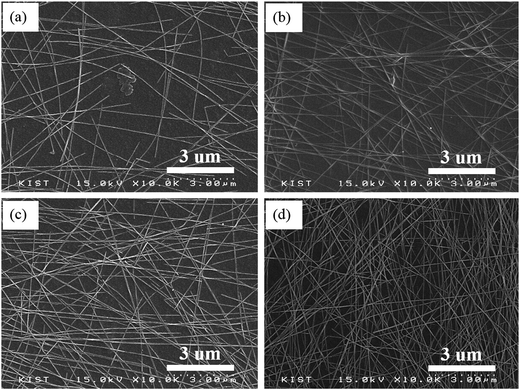 | ||
| Fig. 6 SEM images of the AgNWs as a function of pumping speed: (a) 20 RPM, (b) 30 RPM, (c) 50 RPM and (d) 70 RPM. | ||
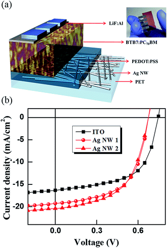
To verify the feasibility of the AgNW mesh transparent electrode, organic solar cells (OSCs) were prepared and their performance was evaluated. The OSCs were fabricated as ordered layers of PEDOT:PSS/PTB7:PC70BM/LiF/Al on the transparent electrodes of AgNWs and ITO, as shown in Fig. 8a. The optoelectronic characteristics of the fabricated OSCs were measured using a solar simulator (ORIEL) with a 150 W light source. The intensity of the standard light source was corrected using a standard Si photodiode to realize the AM 1.5 condition and 100 mW cm−2 intensity. The OSC fabricated on the AgNWs mesh displayed a short circuit current (Jsc) of 20.42 mA cm−2, an open circuit voltage (Voc) of 0.67 V, fill factor (FF) of 0.55 and 7.65% efficiency and showed an improved performance when compared to the ITO-based OSC that showed a Jsc value of 16.36 mA cm−2, Voc = 0.74 V, FF = 0.58 and 7.17% efficiency as, listed in Fig. 8b and Table 2. The AgNW mesh transparent electrode showed good efficiency in the OSC even though it had a lower transmittance compared to that of the ITO-based transparent electrode because of the characteristics of the AgNW mesh, which increased the light scattering and light trapping effect of incoming photons. These results proved that the AgNW mesh transparent electrode can be successfully applied to a flexible optoelectronic element with superior performance when compared to a ITO-based transparent electrode.
| Voc (mV) | Jsc (mA cm−2) | FF | PCE (%) | |
|---|---|---|---|---|
| ITO | 0.74 | −16.36 | 0.58 | 7.17 |
| AgNW 1 | 0.67 | −19.27 | 0.58 | 7.57 |
| AgNW 2 | 0.67 | −20.42 | 0.55 | 7.66 |
4. Conclusion
Transparent electrodes were formed on a PET film using AgNW ink for low-cost mass production using the roll-to-roll slot die technique. When the transparent conductive film was manufactured using the abovementioned AgNW ink using a roll-to-roll the slot die machine, the best coating was obtained in a large area when the shim plate thickness of 30 μm of slot-die was used. Various transparent conductive films were manufactured with low sheet resistance of 32–94 Ω sq−1, haze of 1.3–3.2 and high transmittance of 86.2–92% according to the different gear pumping speeds used. Furthermore, the fabricated AgNW transparent conductive film showed a greater adhesive strength due to the effects of the acrylic resin as the over-coating layer and the polymer dispersant, indicating excellent flexibility. The AgNW transparent conductive film, developed in this study, was found to be the most appropriate material for replacing ITO, and enabled large-area and low-cost production with high flexibility because it was prepared via a roll-to-roll slot die method. Therefore, it can be used to produce flexible solar cells with high-energy conversion efficiency for building outer walls and curved devices, and could bring about great changes to the solar cell market. Moreover, due to the low surface roughness and excellent electrical and optical properties, the AgNW transparent electrodes may be applicable to various flexible electronic devices including low-cost organic solar cells and OLEDs.Acknowledgements
The authors would like to thank the financial support from the KIST Institution Program (program No. 2E26390) and Basic Science Research Program through the National Research Foundation of Korea (NRF) funded by the Ministry of Science, ICT & Future Planning (2016R1C1B2012136).References
- D. S. Ginley, H. Hosono, and D. C. Paine, Handbook of transparent conductors, 2011 Search PubMed.
- S. Kiruthika, R. Gupta, A. Anand, A. Kumar and G. U. Kulkarni, ACS Appl. Mater. Interfaces, 2015, 7, 27215 CAS.
- H. Wu, D. Kong, Z. Ruan, P. C. Hsu, S. Wang, Z. Yu, T. J. Carney, L. Hu, S. Fan and Y. Cui, Nat. Nanotechnol., 2013, 8, 421 CrossRef CAS PubMed.
- S. Bae, H. Kim, Y. Lee, X. Xu, J. S. Park, Y. Zheng, J. Balakrishnan, T. Lei, H. R. Kim, Y. I. Song, Y. J. Kim, K. S. Kim, B. Özyilmaz, J. H. Ahn, B. H. Hong and S. Iijima, Nat. Nanotechnol., 2010, 5, 574 CrossRef CAS PubMed.
- C. Sachse, N. Weiss, N. Gaponik, L. Mueller-Meskamp, A. Eychmueller and K. Leo, Adv. Energy Mater., 2014, 4, 1300737 CrossRef.
- S. Kiruthika, K. D. M. Rao, A. Kumar, R. Gupta and G. U. Kulkarni, Mater. Res. Express, 2014, 1, 026301 CrossRef.
- M. Song, D. S. You, K. Lim, S. Park, S. Jung, C. S. Kim, D. H. Kim, D. G. Kim, J. K. Kim, J. Park, Y. C. Kang, J. Heo, S. H. Jin, J. H. Park and J. W. Kang, Adv. Funct. Mater., 2013, 23, 4177 CrossRef CAS.
- J. Y. Lee, S. T. Connor, Y. Cui and P. Peumans, Nano Lett., 2008, 8, 689 CrossRef CAS PubMed.
- B. E. Hardin, W. Gaynor, I. K. Ding, S. B. Rim, P. Peumans and M. D. McGehee, Org. Electron., 2011, 12, 875 CrossRef CAS.
- J. Lee, P. Lee, H. Lee, D. Lee, S. S. Lee and S. H. Ko, Nanoscale, 2012, 4, 6408 RSC.
- S. M. Bergin, Y. H. Chen, A. R. Rathmell, P. Charbonneau, Z. Y. Li and B. J. Wiley, Nanoscale, 2012, 4, 1996 RSC.
- ICT Sector Focus Report, Printed Electronics, Spinverse, 2010, p. 1 Search PubMed.
- A. Curtis and C. Wilkinson, Trends Biotechnol., 2001, 19, 97 CrossRef CAS PubMed.
- Y. Galagen, R. Andriessen, E. Rubingh, N. Grossiord, P. Blom, S. Veenstra, W. Verhees and J. Kroon, Lope-C., 2010, p. 88 Search PubMed.
- M. Jørgensen, K. Norrman and F. Krebs, Sol. Energy Mater. Sol. Cells, 2008, 2831, 88 Search PubMed.
- F. C. Krebs, Sol. Energy Mater. Sol. Cells, 2009, 93, 1636 CrossRef CAS.
- S. Khan, S. Tinku, L. Lorenzelli and R. S. Dahiya, IEEE Sens. J., 2015, 15, 3146 CrossRef CAS.
- O. J. Romero, W. J. Suszynski, L. E. Scriven and M. S. Carvalho, J. Non-Newtonian Fluid Mech., 2004, 118, 137 CrossRef CAS.
- L. Y. L. Wu, W. T. Kerk and C. C. Wong, Thin Solid Films, 2013, 544, 427 CrossRef CAS.
- T. J. Faircloth, J. G. Innocenzo and C. D. Lang, Slot Die Coating for OLED Displays, SID Symposium Digest 29, 2008, pp. 645–647 Search PubMed.
- Y. R. Chang, H. M. Chang, C. F. Lin, T. J. Liu and P. Y. Wu, J. Colloid Interface Sci., 2007, 308, 222 CrossRef CAS PubMed.
- B. Y. Wang, T. H. Yoo, J. W. Lim, B. I. Sang, D. S. Lim, W. K. Choi, D. K. Hwang and Y. J. Oh, Small, 2015, 11, 1905 CrossRef CAS PubMed.
- L. Qiao, D. Wang, L. Zuo, Y. Ye, J. Qian, H. Chen and S. He, Appl. Energy, 2011, 88, 848 CrossRef CAS.
- B. J. Park, B. O. Park, B. H. Ryu, Y. M. Choi, K. S. Kwon and H. J. Choi, J. Appl. Phys., 2010, 108, 102803 CrossRef.
- B. Y. Wang, T. H. Yoo, Y. W. Song, D. S. Lim and Y. J. Oh, ACS Appl. Mater. Interfaces, 2013, 5, 4113 CAS.
- A. M. Gaikwad, G. L. Whiting, D. A. Steingart and A. C. Arias, Adv. Mater., 2011, 23, 3251 CrossRef CAS PubMed.
- T. Stubhan, J. Krantz, N. Li, F. Guo, I. Litzov, M. Steidl, M. Richter, G. J. Matt and C. J. Brabec, Sol. Energy Mater. Sol. Cells, 2012, 107, 248 CrossRef CAS.
Footnote |
| † Electronic supplementary information (ESI) available. See DOI: 10.1039/c6ra26595b |
| This journal is © The Royal Society of Chemistry 2017 |

