 Open Access Article
Creative Commons Attribution 3.0 Unported Licence
Broadband localized electric field enhancement produced by a single-element plasmonic nanoantenna
Zhengdong Yonga,
Chensheng Gonga,
Yongjiang Donga,
Senlin Zhanga and
Sailing He *ab
*ab
aCentre for Optical and Electromagnetic Research, State Key Laboratory of Modern Optical Instrumentations, Zhejiang University, Hangzhou 310058, China. E-mail: sailing@kth.se
bDepartment of Electromagnetic Engineering, School of Electrical Engineering, Royal Institute of Technology (KTH), S-100 44 Stockholm, Sweden
First published on 12th January 2017
Abstract
We propose a novel design of a broadband plasmonic nanoantenna, investigate it numerically using finite-difference time-domain methods, and explain its performance using the analysis of charge distribution in addition to a multipole expansion. The custom-designed single-element nanoantenna consists of a modified gold ring structure with a bowtie-shaped spike inside. In contrast to the spectral response of extinction, the broadband localized electric field intensity enhancement is achieved over a bandwidth of 850 nm in the near infrared spectrum. Up to 26- and 22-fold field enhancements near the bowtie spike are obtained at the peak and even in the dip region of the extinction spectrum, respectively. Moreover, the nanostructure exhibits high tunability of its spectral features by modifying the structural parameters. We further demonstrate that the proposed nanoantenna can provide broadband spontaneous emission rates and quantum efficiency enhancements when a low-quantum efficiency emitter is introduced.
Introduction
Inspired by radio and microwave antennas, optical antennas operating at visible and near-infrared frequencies have emerged as a powerful tool in nano-optics, as they can efficiently link free-propagating light with localized fields at the nanometer scale.1,2 Due to the localized surface plasmon resonances arising from the collective oscillation of free electrons in metals, optical antennas allow for large electromagnetic field enhancement, deep subwavelength confinement of light, and tailoring of the local density of photonic states.3,4 These promising abilities have ignited the development of a vast variety of applications, including surface-enhanced Raman scattering spectroscopy,5,6 fluorescence enhancement,7,8 optical manipulation9,10 and nonlinearity.11,12 As the resonance decisively depends on the shape, dimensions, and material of the antenna, a large variety of plasmonic antenna structures have been proposed, such as nanorods,13 bow-ties,14 nanorings,15 and Yagi-Uda antennae.16 Though all of these antennas have demonstrated the ability to confine light in the nanoscale and strongly enhance local fields, their narrow-band spectra with sharp resonances are a major challenge for applications that require devices operating over a wide range of frequencies. For example, antennas operating over a wide frequency spectrum are essential to improve energy harvesting efficiency of photovoltaic devices.17,18 Broadband optical antennas are also highly desirable for surface enhanced Raman scattering, fluorescence enhancement, and higher harmonic generation, which are intrinsically multi-wavelength and broadband in nature.6,19,20To surpass the inherently limited narrow-band operation of infrared frequencies, several topologies have been explored, such as antennas with long aspect radio,21,22 fractal geometry,23,24 multiple-segment arrangements,25,26 wavelength-size 2D structures27 and log-periodic antennas.20,28,29 However, they all have some limitations; for instance, the locations of hot spots in fractal antennas23 are wavelength-dependent, the bandwidth of multiple dipole antennas is constrained to the number of resonant elements,25 and photonic-plasmonic antennas require particle arrays of multiple periods, leading to impractically large footprints.26 Recently, analogous to the microwave designs of broadband antennas, trapezoidal log-periodic antennas have been proposed and used for multispectral applications.20,30 Coupled antennas are also good candidates for broadband operation.31,32 However, all the nanoantenna designs in literature require at least two separated elements. These disconnected structures can only be fabricated on substrates, which hampers their biochemistry applications in aqueous solutions or in vivo. Though the coupled antennas provide a much higher field intensity, for some practical applications (i.e., fluorescence enhancement of fluorophores), high excitation intensities are often detrimental to their efficiency and photostability.33 Furthermore, the small sizes of the hot spots of coupled antennas limit the interaction to just a few emitters and prevent the development of large-area chips. For these reasons, it is of great significance and remains a great challenge to design a single-element broadband plasmonic nanoantenna with larger hot spot areas.
In this paper, we have proposed a single-element modified ring nanostructure which provides broadband localized field enhancement in the same spatial position. The spectral responses of the nanoantenna in terms of cross sections and field enhancement near the tip are first studied. Then, the analysis of charge distributions and multipole expansions are performed to investigate the underlying physics. Finally, broadband spontaneous emission rates and quantum efficiency enhancements are demonstrated when a quantum emitter is placed inside the nanoantenna. Such single-element broadband antennas will hold great potential in many applications, such as nanolasers, biosensors, surface enhanced Raman scattering, and nonlinear optics.
Methods
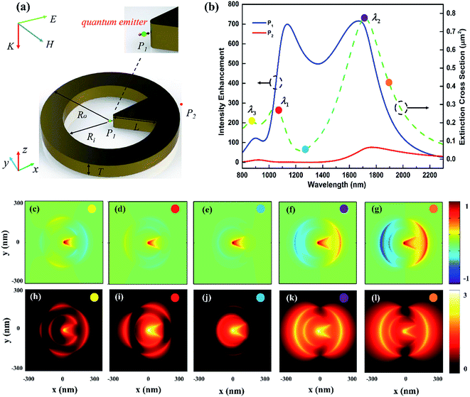
Three-dimensional finite-difference time-domain calculations were performed using commercially available software package (Lumerical FDTD Solutions Inc. v8.6) to investigate the optical properties of the antenna. Fig. 1(a) shows the schematic of our proposed single-element broadband plasmonic nanostructure. It is represented by a modified gold ring resonator with a bowtie-shaped spike inside. The relevant structural parameters are the bowtie's length L, opening angle θ, the inner radius Rin, and the outer radius Rout of the ring. Considering the fabrication limits, and in order to avoid sharp edges that are difficult to fabricate, we model the bowtie's tip as rounded with a radius of curvature of 10 nm. In the following, the typical geometrical parameters are chosen; namely, L = 110 nm, θ = 50°, Rin = 110 nm, Rout = 180 nm, and the height T of the antenna is 40 nm.To first study the optical properties of the single antenna, a total-field scattered-field (TFSF) source polarized along the x-direction was normally-incident to it, as shown in Fig. 1(a). Perfectly matched layers were employed in every face of the simulation box. Mesh override regions covering different volumes of the structure were used for fine resolution of the structure. Specifically, a mesh size of 0.5 nm was used near the bowtie's tip and 1 nm for other regions. Near field distributions were recorded by field monitors, and the extinction cross section was calculated by the sum of the scattering and absorption cross sections.3 Then, for the simulation of the emission process modified by the nanoantenna, a point dipole source oriented in the x-direction (considered as an isolated emitter) is placed inside the nanoantenna. The radiated emitted power Prad and the total emitted power Ptot in the presence of the antenna were calculated by integrating the power flow over a closed surface surrounding the dipole source at respective distances of 1 μm and 5 nm. The total and radiative decay rates enhancement (Γrad = Prad/P0 and Γtot = Ptot/P0) can then be obtained by normalizing the emitted power with the radiated emitted power P0 of the same dipole source in the absence of the antenna.4
Finally, to further understand the origin of the spectral response of the nanoantenna, we perform a multipole expansion34 of the total scattering response of the nanoantenna for plane wave excitation, according to
 | (1) |
Results and discussion
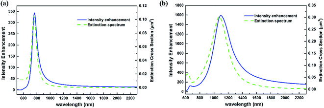
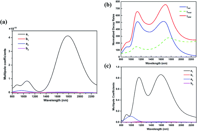
The near field intensity enhancements with respect to the corresponding incident field at the two monitoring points P1 and P2 (5 nm distant from the tip and ring marked in Fig. 1) and the extinction cross-sections of the single nanoantenna are plotted in Fig. 1(b). It is evident that our plasmonic nanoantenna has two pronounced extinction peaks around λ1 = 1100 nm and λ2 = 1700 nm. A lower peak around λ3 = 850 nm is also presented in both the extinction and near field intensity spectrum. Most interestingly, in contrast to the extinction characteristics, we observe a relatively large field intensity enhancement at P1 over a broad spectral range, and the full-width-half-maximum (FWHM) bandwidth is about 850 nm. Up to 26- and 22-fold field enhancements near the bowtie spike are obtained at the peak and even in the dip region of the extinction spectrum, respectively. In addition, this broadband behavior can only be observed inside the modified ring. To understand the operating principle of the nanoantenna, the charge distribution analysis of the plasmonic modes at specific wavelengths are performed. A simple way of visualizing the charges is to calculate the normal component of the electric field Ez on a plane 2 nm above the structure since the field component is not contained in the illumination and orientation is directly related to the sign of the charges.37 As clearly shown in Fig. 1(c), the related mode profile at λ3 can be assigned to a quadrupole-like oscillation. Due to the symmetry breaking, induced by the additional bowtie spike, this usual dark mode can be directly excited by normal incidence. With regard to the resonance around λ1 shown in Fig. 1(i), the strong field is mainly concentrated around the bowtie spike. From Fig. 1(f) and (k), a typical symmetric mode of the modified ring around the resonance λ2 and strong field around the ring can be observed.15 Particularly, for the electron oscillations corresponding to the dip of the extinction spectrum in Fig. 1(e), the total dipole moment (observed at the far field) is much smaller, but a large near field enhancement inside the nanoantenna can still be produced as shown in Fig. 1(j) and the charges are mainly localized near the bowtie tips. These charge distribution analysis can provide us with an intuitive understanding of the plasmonic modes of the proposed nanoantenna. The additional bowtie spike inside the nanoring serves as an electron reservoir and enables the focalization of electric fields at its apex due to the lightning rod effect.38,39 To further evaluate the performance of the proposed antenna, we also compare it to the isolated nano-triangle with the same dimensions as the one protruding inside the ring and the popular bowtie design for a wavelength of 1100 nm. The isolated nano-triangle has a resonant peak around 800 nm in Fig. 2(a), with FWHW about 100 nm, which is much narrower than our proposed structure. Thus the nanoring plays a critical role in this broadband antenna. Fig. 2(b) also shows the spectral response of bowtie antennas.14 We find a 40-fold electric field enhancement at resonance with a bandwidth of 300 nm.In order to further investigate the origin of the spectral response of our antennas, a multipole analysis is performed for both plane wave and dipole excitation. The results of the non-negligible coefficients for plane waves are presented in Fig. 3(a). The a2 coefficient, corresponding to an electric quadrupole contribution, shows a resonant behavior around the operation wavelength λ3. This is consistent with the charge distribution analysis in Fig. 1(c). Furthermore, the two resonant peaks of the extinction spectrum around λ1 and λ2 mainly originate from the electric dipole contribution. The small electric dipole moment between these two resonances results in the dip in the extinction spectrum. In fact, we can comprehend the interaction between the designed structure and light wave by considering the antenna as simply two coupled dipolar resonators. Their mode profiles on resonance are shown in Fig. 1(d) and (f). We note again here that a dipolar resonance is characterized by a phase that matches the phase of the incident field on one side of the resonance and is out-of-phase on the other side. In our case, where the two dipolar resonances have different resonant frequencies, there will be some regions of the spectrum where they are in phase or out of phase, forming a higher radiant mode (constructive interference) or a lower radiant mode (destructive interference). The interaction between two bright dipolar modes has recently been studied in the far field region, and the destructive interference gives rise to the Fano resonance.40 However, interference of the incident and scattered light waves generates a more complex near-field pattern. In particular, it is the near field enhancement and not the extinction properties of the antenna that influences the efficiency of SERS or fluorescence. We may qualitatively attribute the broadband localized field enhancement to the near field constructive interference of the two dipolar resonances. To evaluate it more quantitatively, due to the reciprocity theorem,2 we calculate the normalized decay rates for an on-axis x-oriented dipole located at P1 and use the same multipole expansion of the radiated field as before.41 An expected broadband radiative decay rate is shown in Fig. 3(b). More importantly, we emphasize that the dominant contribution of the electric dipole to the radiative decay rate is broadband for dipole excitation in Fig. 3(c), in contrast to that of plane wave excitation. By using multipole expansion, it aptly explains the different spectral responses between the far field and the near field.
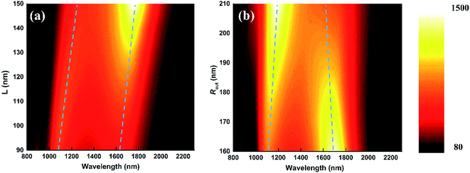
As mentioned above, the structural parameters of the nanoantenna are critical for its optical properties. Some parametric studies are performed to give us insights as to how they affect the performance of the nanoantenna. Fig. 4(a) and (b) illustrate the near field intensity spectrum at P1 when L and Rout are changed, respectively, while other parameters are kept the same. More than one order of localized electric field enhancement over a broadband spectral range, up to 1000 nm, can be observed in all the studies. From Fig. 4(a), one sees an obvious red-shift of the two resonant peaks and an increasing intensity enhancement of the long wavelength resonance as the length L increases. While in Fig. 4(b), as Rout increases from 160 nm to 210 nm, the two pronounced resonances of the near field intensity enhancement gradually contract to the center wavelength, with the strength at the short wavelength increases and the other decreases. This is due to a decreasing coupling strength between the inner and outer surfaces of the nanoring.15 Therefore, both the length L of the bowtie spike and the outer radius Rout of the ring need to be carefully designed to engineer the near field of the nanoantenna.
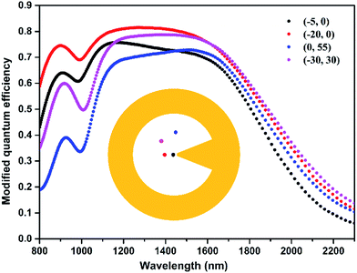
Inspired by the broadband localized field enhancement in the modified ring nanoantenna, we propose its potential application for controlling the radiative properties of quantum emitters. As was first studied by Purcell, the radiation dynamic of quantum emitters can be modified by the local density of the optical states.4,42,43 A representative broadband and large Purcell enhancement with a bandwidth of 800 nm is shown in Fig. 3(b), which has never been achieved by a single-element nanostructure so far. In the spectral range of interest, the non-radiative decay rates due to metal loss are much smaller than the radiative rates, which result in a high quantum efficiency. As the total fluorescence enhancement is a product of field enhancement factor in the excitation process and quantum efficiency enhancement in the emission process, it is necessary to study the modified quantum efficiency of a quantum emitter by our proposed broadband nanoantenna. Previous studies have demonstrated that low-quantum efficiency emitters have much higher fluorescence enhancement than high-quantum efficiency emitters because their intrinsic quantum efficiency has a greater potential to be improved by the presence of the nanoantenna.44 In our studies, we set the tip of the bowtie spike as the origin of the coordinates and assume a quantum emitter located at different positions inside of the typical nanoantenna with intrinsic quantum efficiency η0 = 0.25. The modified quantum efficiency η related to η0 is calculated according to  , and shown in Fig. 5. It is obvious that the modified quantum efficiency of a quantum emitter is highly improved by the nanoantenna, and all the curves depict a broadband quantum efficiency enhancement. It indicates that the structure has a large active volume, allowing for collective coupling of many quantum emitters in a reproducible and predictable manner. Compared to the traditional nanoring structure,45 the additional bowtie spike inside can broaden the spectral response of the near field and provides a much larger intensity enhancement due to a “lightning rod effect”. As a result, the proposed single-element nanoantenna is very promising for practical applications.
Conclusions
In summary, we have presented and demonstrated by employing FDTD calculations an efficient strategy to engineer broadband localized field enhancement in the same spatial area. Specifically, by introducing a bowtie spike inside the nanoring, the single-element nanoantenna shows a large near field intensity enhancement for an 850 nm bandwidth in the near-infrared spectrum. Up to 26- and 22-fold field enhancements near the bowtie spike are obtained at the peak and even in the dip region, respectively, of the extinction spectrum. The analysis of the charge distribution and multipole expansion clearly reveal the origin of the spectral response of the nanoantenna. By identifying its multipolar nature, the dominant electric dipolar contributions give rise to the different spectral responses between the near field and the far field. In addition, the nanostructure exhibits high tunability of its spectral features by modifying geometrical parameters. From the application point of view, the proposed nanoantenna has great potential in controlling the radiative properties of a quantum emitter. The strong field enhancement inside the nanoantenna simultaneously enables high Purcell and broadband quantum efficiency enhancement of quantum emitters, outperforming that of traditional plasmonic rings and dimmer antennas. These finding provides a new design strategy for broadband localized field enhancement, such as the design of the same ring but with two bowtie spikes facing each other. It could be exploited for a range of other applications, such as harmonic generation and nanolasers.46Acknowledgements
This work was partially supported by the National Natural Science Foundation of China (No. 91233208 and 61178062), the National High Technology Research and Development Program (863 Program) of China (No. 2013AA014401), the Program of Zhejiang Leading Team of Science and Technology Innovation, and Swedish VR grant (No. 621-2011-4620).Notes and references
- L. Novotny and N. van Hulst, Nat. Photonics, 2011, 5, 83–90 CrossRef CAS.
- P. Biagioni, J. S. Huang and B. Hecht, Rep. Prog. Phys., 2012, 75, 024402 CrossRef PubMed.
- S. A. Maier, Plasmonics: fundamentals and applications, Springer, 2007 Search PubMed.
- L. Novotny and B. Hecht, Principles of nano-optics, Cambridge University Press, 2006 Search PubMed.
- J. Xie, Z. Q. Zhang, J. Y. Lee and D. I. C. Wang, ACS Nano, 2008, 2, 2473–2480 CrossRef CAS PubMed.
- Y. Chu, M. G. Banaee and K. B. Crozier, ACS Nano, 2010, 4, 2804–2810 CrossRef CAS PubMed.
- P. Anger, P. Bharadwaj and L. Novotny, Phys. Rev. Lett., 2006, 96, 113002 CrossRef PubMed.
- A. Kinkhabwala, Z. Yu, S. Fan, Y. Avlasevich, K. Müllen and W. E. Moerner, Nat. Photonics, 2009, 3, 654–657 CrossRef CAS.
- W. Zhang, L. Huang, C. Santschi and O. J. F. Martin, Nano Lett., 2010, 10, 1006–1011 CrossRef CAS PubMed.
- K. Wang, E. Schonbrun, P. Steinvurzel and K. B. Crozier, Nat. Commun., 2011, 2, 469 CrossRef PubMed.
- K. Thyagarajan, S. Rivier, A. Lovera and O. J. F. Martin, Opt. Express, 2012, 20, 12860–12865 CrossRef PubMed.
- H. Aouani, M. Rahmani, M. Navarro-Cía and S. A. Maier, Nat. Nanotechnol., 2014, 9, 290–294 CrossRef CAS PubMed.
- P. Mühlschlegel, H.-J. Eisler, O. J. F. Martin, B. Hecht and D. W. Pohl, Science, 2005, 308, 1607–1609 CrossRef PubMed.
- P. J. Schuck, D. P. Fromm, A. Sundaramurthy, G. S. Kino and W. E. Moerner, Phys. Rev. Lett., 2005, 94, 017402 CrossRef CAS PubMed.
- J. Aizpurua, P. Hanarp, D. S. Sutherland, M. Käll, G. W. Bryant and F. J. García de Abajo, Phys. Rev. Lett., 2003, 90, 057401 CrossRef CAS PubMed.
- T. H. Taminiau, F. D. Stefani and N. F. van Hulst, Opt. Express, 2008, 16, 10858–10866 Search PubMed.
- M. A. Green and S. Pillai, Nat. Photonics, 2012, 6, 130 CrossRef CAS.
- H. A. Atwater and A. Polman, Nat. Mater., 2010, 9, 205–213 CrossRef CAS PubMed.
- G. Lu, J. Liu, T. Zhang, H. Shen, P. Perriat, M. Martini, O. Tillement, Y. Gu, Y. He, Y. Wang and Q. Gong, Nanoscale, 2013, 5, 6545–6551 RSC.
- M. Navarro-Cia and S. A. Maier, ACS Nano, 2012, 6, 3537–3544 CrossRef CAS PubMed.
- J. Dorfmuller, R. Vogelgesang, W. Khunsin, C. Rockstuhl, C. Etrich and K. Kern, Nano Lett., 2010, 10, 3596–3603 CrossRef PubMed.
- B. N. Khlebtsov and N. G. Khlebtsov, J. Phys. Chem. C, 2007, 111, 11516–11527 CAS.
- G. Volpe, G. Volpe and R. Quidant, Opt. Express, 2011, 19, 3612–3618 CrossRef CAS PubMed.
- R. U. Tok and K. Şendur, Opt. Lett., 2014, 39, 6977–6980 CrossRef PubMed.
- E. S. Ünlü, R. U. Tok and K. Şendur, Opt. Express, 2011, 19, 1000–1006 CrossRef PubMed.
- R. Blanchard, S. V. Boriskina, P. Genevet, M. A. Kats and F. Capasso, Opt. Express, 2011, 19, 22113–22124 CrossRef PubMed.
- C. Kan, X. Zhu and G. Wang, J. Phys. Chem. B, 2006, 110, 4651–4656 CrossRef CAS PubMed.
- R. S. Pavlov, A. G. Curto and N. F. van Hulst, Opt. Commun., 2012, 285, 3334–3340 CrossRef CAS.
- J. Yang, F. Kong, K. Li and S. Sheng, Opt. Commun., 2015, 342, 230–237 CrossRef CAS.
- H. Aouani, M. Rahmani, H. Šípová, V. Torres, K. Hegnerová, M. Beruete and S. A. Maier, J. Phys. Chem. C, 2013, 117, 18620–18626 CAS.
- R. Zhou, J. Ding, B. Arigong, Y. Lin and H. Zhang, J. Appl. Phys., 2013, 114, 184305 CrossRef.
- Z. D. Yong, S. Zhang, Y. Dong and S. He, Prog. Electromagn. Res., 2015, 153, 123–131 CrossRef.
- K. M. Dyumaev, A. A. Manenkov, A. P. Maslyukov, G. A. Matyushin, V. S. Nechitailo and A. M. Prokhorov, J. Opt. Soc. Am. B, 1992, 9, 143–151 CrossRef CAS.
- P. Grahn, A. Shevchenko and M. Kaivola, New J. Phys., 2012, 14, 093033 CrossRef.
- A. Vial, A.-S. Grimault, D. Macias, D. Barchiesi and M. L. de la Chapelle, Phys. Rev. B: Condens. Matter Mater. Phys., 2005, 71, 085416 CrossRef.
- P. B. Johnson and R. W. Christy, Phys. Rev. B: Solid State, 1972, 6, 4370–4379 CrossRef CAS.
- C. Rockstuhl, F. Lederer, C. Etrich, T. Zentgraf, J. Kuhl and H. Giessen, Opt. Express, 2006, 14, 8827–8836 CrossRef PubMed.
- D. Wang, T. Yang and K. B. Crozier, Opt. Express, 2010, 18, 10388–10394 CrossRef PubMed.
- A. Li and S. Li, Nanoscale, 2014, 6, 12921–12928 RSC.
- A. Lovera, B. Gallinet, P. Nordlander and O. J. Martin, ACS Nano, 2013, 7, 4527–4536 CrossRef CAS PubMed.
- E. Rusak, I. Staude, M. Decker, J. Sautter, A. E. Miroshnichenko, D. A. Powell and Y. S. Kivshar, Appl. Phys. Lett., 2014, 105, 221109 CrossRef.
- E. M. Purcell, Phys. Rev., 1946, 69, 681 CrossRef.
- P. Fauché, S. Ungureanu, B. Kolaric and R. A. Vallée, J. Mater. Chem. C, 2014, 2, 10362–10368 RSC.
- L. Rogobete, F. Kaminski, M. Agio and V. Sandoghdar, Opt. Lett., 2007, 32, 1623–1625 CrossRef PubMed.
- A. Rakovich, P. Albella and S. A. Maier, ACS Nano, 2015, 9, 2648–2658 CrossRef CAS PubMed.
- M. A. Noginov, G. Zhu, A. M. Belgrave, R. Bakker, V. M. Shalaev, E. E. Narimanov and U. Wiesner, Nature, 2009, 460, 1110–1112 CrossRef CAS PubMed.
| This journal is © The Royal Society of Chemistry 2017 |

