 Open Access Article
Creative Commons Attribution 3.0 Unported Licence
Mixed conduction in BaF2 nanocrystals under high pressure
Xiaoyan Cuia,
Tingjing Hu *a,
Jingshu Wanga,
Junkai Zhanga,
Rui Zhaob,
Xuefei Lia,
Jinghai Yanga and
Chunxiao Gao*c
aKey Laboratory of Functional Materials Physics and Chemistry of the Ministry of Education, Jilin Normal University, Siping 136000, Jilin, China. E-mail: tjhumars@126.com
bJilin Provincial Key Laboratory for Numerical Simulation, Jilin Normal University, Siping 136000, Jilin, China
cState Key Laboratory of Superhard Materials, Jilin University, Changchun 130012, China. E-mail: cc060109@qq.com
First published on 20th February 2017
Abstract
The charge transport behavior of barium fluoride nanocrystals has been investigated by in situ impedance measurement up to 23 GPa. It was found that the parameters changed discontinuously at each phase transition. The charge carriers in BaF2 nanocrystals include both F− ions and electrons. Pressure makes both the F− ions diffusion and electronic transport more difficult. The defects at grains dominate the electronic transport process. Pressure could make the charge–discharge processes in the Fm3m and Pnma phases more difficult. The electron conduction plays a dominant role in the transport process. In the Fm3m and Pnma phases, the electron transference number increases with increasing pressure.
Introduction
The alkaline earth fluorides are an important class of materials that form the basis of a range of applications in geosciences, materials science, and condensed-matter physics.1,2 In terms of the applications, the alkaline earth fluorides have attracted considerable interest due to their unique properties, including low-energy phonons, high ionicity, electron-acceptor behavior, high resistivity, and anionic conductivity.3–5 Barium fluoride (BaF2) is an important member of alkaline-earth fluorides and has been extensively studied for its intrinsic optical properties.6–8 Specifically, it is the fastest luminescent material that has been found to date,9 thereby making it an ideal high-density luminescent material for applications in gamma ray and elementary particle detectors.10 Recently, BaF2 has also been found to exhibit superionic conductivity by dissolving appropriate impurities into the lattice or by introducing an interface that causes the redistribution of ions in the space-charge region,11 and is therefore considered as a candidate material for high temperature batteries, fuel cells, chemical filters and sensors.11BaF2 is a typical anionic conductivity material; therefore its conductive property is an interesting subject. Sorokin et al.12 studied the anionic transport in single crystals of the nominally pure BaF2. They found that the microscopic origin of the anionic conductivity depends mainly on the nature of the defect structure in the solid solutions.12 Kanchana et al.13 calculated the electronic band structure of BaF2 and predicted that it undergoes metallization around 33 GPa. Nanoscale materials attract particular interest not only for their unique enhanced properties, which are different from those of the bulk materials, but also for their fundamental scientific and technological applications.14,15 Generally speaking, a decrease in crystal size implies an increased proportion of the surfaces (interfaces) and usually also in increased grain boundary (GB) properties. Therefore, the nanoscale material may have some unique transport properties that would not be presented in the bulk material, which is worth exploring. The electric conductive of BaF2 nanocrystals are inextricably bound up with the types of the charge carriers (electrons or ions) and their scattering processes both in the grains and the grain boundaries. However, the above-mentioned issues have not been studied in detail.
In this paper, we conduct an alternate-current (AC) impedance measurement of BaF2 nanocrystals under high pressure up to 23 GPa. The conduction mechanism involved in the charge transport process was studied.
Experiments
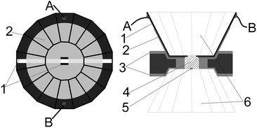
High pressure was generated by a Mao-Bell-type Diamond anvil cell (DAC), and the culet of the diamond anvil was 400 μm in diameter. A thin film of metal molybdenum was deposited on the surface of the cell by magnetron sputtering system, and then patterned into microcircuit with two sections by photoetching. Above the microcircuit, a film of aluminium oxide was sputtered to protect the microcircuit. The electrode ends were in exposure by removing the aluminium oxide chemically to make the probes contact the sample and connect to the electric meters. A detection window (120 × 120 μm) was created in the center of the diamond culet. The distance between electrodes was 50 μm. The technical process of the microcircuit fabrication has been reported by previous paper.16–18 The completed microcircuit and the profile of our designed DAC are shown in Fig. 1.A T301 stainless steel was pre-indented into 60 μm in thickness. Using the laser drilling machine, a hole of 250 μm in diameter was drilled at the centre of indentation. Then, the insulating layer that mixed cubic boron nitride powder and epoxy was compressed into the indentation. Subsequently, a sample chamber of 150 μm was drilled. Pressure was calibrated by R1 fluorescence peak of ruby. To avoid additional error on the electrical transport measurements, no pressure-transmitting medium was used. The impedance spectroscopy was measured by a Solartron 1260 impedance analyser equipped with Solartron 1296 dielectric interface. Sine signal with amplitude of 1 V and frequency ranged from 0.1 to 107 Hz was applied into the sample.
The BaF2 nanocrystals were prepared by a liquid-solid-solution (LSS) solvothermal route. The TEM image and particle size distribution histograms of the BaF2 nanocrystals were shown in Fig. 2.19 The sample is a square shaped with a mean size of length around 19 ± 3 nm. High pressure synchrotron radiation X-ray diffraction patterns of BaF2 nanocrystals were shown in Fig. 3.19 It can be seen that BaF2 nanocrystals undergo two phase transformations from Fm3m to Pnma structure at 5.8 GPa, and then to P63/mmc structure at 14.4 GPa. The detail discussion was in ref. 19.
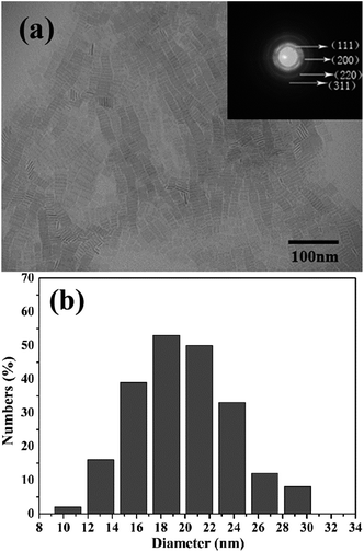 | ||
| Fig. 2 (a) TEM images of the as-synthesized BaF2 nanocrystals; (b) particle size distribution histograms of the BaF2 nanocrystals. | ||
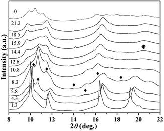 | ||
| Fig. 3 X-ray diffraction patterns of BaF2 nanocrystals under high pressure. Diamonds indicate the orthorhombic phase diffraction peaks. The asterisk indicates the hexagonal phase diffraction peak. | ||
Results and discussion
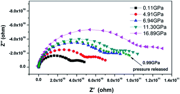
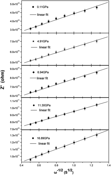
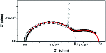
The Nyquist representation of the impedance spectroscopy of BaF2 nanocrystals under various pressures was shown in Fig. 4.As accepted for solid sample, the equivalent circuit method is a reliable approach to describe the impedance spectra. In order to analyze the ionic conduction of F−, the Nyquist representation was replotted into a Z′–ω−1/2 plots as shown in Fig. 5. A linear relation between Z′ and ω−1/2 was found in the low frequency region, indicating that there exists the diffusion of F− ions through the grain boundaries at low frequency. Thus, considering the ionic conduction, a Warburg impedance element to describe the diffusion of the F− ions has been added to the equivalent circuit diagram. If the charge carriers are only F− ions, the impedance spectroscopy would be shown as the hollow circle plot in Fig. 6. Therefore, the charge carriers in BaF2 nanocrystals include both ions and electrons. The equivalent circuit was used as shown in Fig. 7.
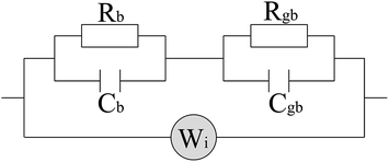 | ||
| Fig. 7 Circuit diagram equivalent to the conduction mechanism. The subscripts of the RC combinations are b for bulk, gb for grain boundary, and Wi denotes the Warburg impedance. | ||
The agreement of the simulated spectra with the experimental data [Fig. 6] indicates the validity of considering both the ionic and electric conductions in BaF2 nanocrystals. The relaxation frequency of grains (fb) can be obtained from the relationship of imaginary part Z′′ versus frequency. The bulk resistance, grain boundary resistance and grain relaxation frequency were shown in Fig. 8.
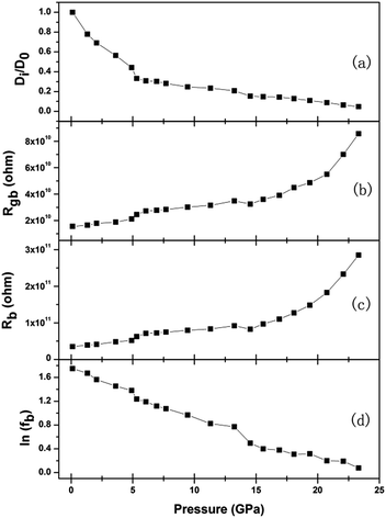 | ||
| Fig. 8 Relationships of diffusion coefficient, bulk and grain boundary resistance, bulk relaxation frequency versus pressure. D0 represents the diffusion coefficient at 0.11 GPa. | ||
To the ionic conduction, the relation between Z′ and ω−1/2 in the low frequency region can be expressed as:
| Z′ = Z′0 + σω−1/2, |
where R is the ideal gas constant, T is temperature, F is Faraday constant, C is F− ions molar concentration. The F− ions diffusion coefficient at 0.11 GPa was set as D0, and the curve Di/D0 under various pressures was shown in Fig. 8(a).
From Fig. 8, it can be seen that each parameter changes discontinuously at about 5.3 and 14.5 GPa. Because BaF2 nanocrystals undergo two phase transformations from Fm3m to Pnma structure at 5.8 GPa, and then to P63/mmc structure at 14.4 GPa,19 the discontinuous changes can be attributed qualitatively to the pressure-induced structural phase transition. These results show that the phase transition is accompanied by the detectable changes in the electrical transport behavior.
Under compression, the F− ions diffusion coefficient of Fm3m and Pnma phases decrease, while the grain resistance and the grain boundary resistance increase; these indicate that the pressure makes both the F− ions diffusion and electronic transport more difficult. In the whole pressure range, the grain resistance shows a relatively larger contribution to the total resistance, as compared to the grain boundary resistance, which indicates that the defects at grains dominate the electronic transport process.
The electron carrier transport in BaF2 nanocrystals grains can be regarded as a charging process in a RC resonance circuit and the relaxation frequency actually denotes the charge–discharge rate of dipoles oscillation process, and its activation energy represents the energy to activate the resonance. The pressure dependent activation energy can be obtained by fitting the pressure dependence of bulk relaxation frequency in Fig. 8(d) to the differential form of Arrhenius equation,
d(ln![[thin space (1/6-em)]](https://www.rsc.org/images/entities/char_2009.gif) fb)/dP = −(1/kBT)(dH/dP), fb)/dP = −(1/kBT)(dH/dP), |
| Pressure region (GPa) | dH/dP (meV GPa−1) |
|---|---|
| 0.11–4.91 | 2.04 |
| 5.32–13.24 | 1.58 |
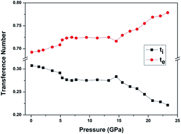
If more than one kind of charge carriers coexist in the materials, it is necessary to clarify which kind of carrier is dominant. The parameter for describing the contributions of one kind of carrier to the transport process is the transference number.20 In the case of BaF2 nanocrystals, there are two kinds of charge carriers, F− ions and the electrons. We define the transference number of F− ion as ti and electron as te. The ti and te can be expressed as:
| ti = (R2 − R1)/R2, |
| te = R1/R2, |
The Nyquist impedance spectrum of BaF2 nanocrystals at 0.11 GPa and 0.99 GPa after pressure release are given in Fig. 4. It can be seen that the pressure effect on the conductive property of BaF2 nanocrystals can be reserved. To the bulk BaF2, the charge carriers are F− ions; while to the BaF2 nanocrystals, the F− ions and the electrons coexist and the electrons is dominant. It can be concluded that both compression and decreasing crystal size treatments are effective methods for improving electron transport in BaF2.
Conclusions
The charge transport behavior of barium fluoride nanocrystals has been investigated by in situ impedance measurement up to 23 GPa. Each parameter changes discontinuously at about 5.3 and 14.5 GPa, corresponding to the phase transitions of BaF2 nanocrystals under high pressure. Pressure makes both the F− ions diffusion and electronic transport more difficult. The defects at grains dominate the electronic transport process. Pressure could make the charge–discharge processes in the Fm3m and Pnma phases more difficult. The electron conduction plays a dominant role in the transport process. In the Fm3m and Pnma phases, the electron transference number increases with increasing pressure. Both compression and decreasing crystal size treatments are effective methods for improving electrons transport in BaF2.Acknowledgements
This work was financially supported by the National Natural Science Foundation of China (Grant Nos 11374131, 11674404, 11404137 and 61378085), Program for New Century Excellent Talents in University (No NCET-13-0824), Program for the development of Science and Technology of Jilin province (Item Nos 201201079, 20150204085GX), and Twentieth Five-Year Program for Science and Technology of Education Department of Jilin Province (Item No. 20150221).Notes and references
- S. M. Dorfman, F. Jiang, Z. Mao, A. Kubo, Y. Meng, V. B. Prakapenka and T. S. Duffy, Phys. Rev. B: Condens. Matter Mater. Phys., 2010, 81, 174121 CrossRef.
- A. Bensalaha, M. Mortiera, G. Patriarcheb, P. Gredinc and D. Vivien, J. Solid State Chem., 2006, 179, 2636 CrossRef.
- C. Feldmann, M. Roming and K. Trampert, Small, 2006, 2, 1248 CrossRef CAS PubMed.
- Z. W. Quan, D. M. Yang, P. P. Yang, X. M. Zhang, H. Z. Lian, X. M. Liu and J. Lin, Inorg. Chem., 2008, 47, 9509 CrossRef CAS PubMed.
- P. Gao, Y. Xie and Z. Li, Eur. J. Inorg. Chem., 2006, 16, 3261 CrossRef.
- E. D. Schmidt and K. Vedam, J. Phys. Chem. Solids, 1966, 27, 1563 CrossRef CAS.
- N. Dutt, O. P. Sharma and J. Shanker, Phys. Status Solidi, 1985, 127, 67 CrossRef CAS.
- J. Kudrnovsky, N. E. Christensen and J. Masek, Phys. Rev. B: Condens. Matter Mater. Phys., 1991, 43, 12597 CrossRef.
- K. Kawano, T. Ohya, T. Tsurumi, K. Katoh and R. K. NakataKawano, Phys. Rev. B: Condens. Matter Mater. Phys., 1999, 60, 11984 CrossRef CAS.
- H. T. Jiang, A. Costales, M. A. Blanco, M. Gu, R. Pandey and J. D. Gale, Phys. Rev. B: Condens. Matter Mater. Phys., 2000, 62, 803 CrossRef CAS.
- N. Sata, K. Eberman, K. Eberl and J. Maier, Nature, 2000, 408, 946 CrossRef CAS PubMed.
- N. L. Sorokin and M. W. Breiter, Solid State Ionics, 1997, 99, 241 CrossRef CAS.
- V. Kanchana, G. Vaitheeswaran and M. Rajagopalan, J. Alloys Compd., 2003, 359, 66 CrossRef CAS.
- F. Zhao and S. Gao, J. Mater. Chem., 2008, 18, 949 RSC.
- M. Chen, J. Kim, J. P. Liu, H. Fan and S. Sun, J. Am. Chem. Soc., 2006, 128, 7132 CrossRef CAS PubMed.
- T. J. Hu, X. Y. Cui, Y. Gao, Y. H. Han, C. L. Liu, B. Liu, H. W. Liu, Y. Z. Ma and C. X. Gao, Rev. Sci. Instrum., 2010, 81, 115101 CrossRef PubMed.
- G. H. Li, Y. Li, M. Zhang, Y. Z. Ma, Y. M. Ma, Y. H. Han and C. X. Gao, RSC Adv., 2014, 4, 42523 RSC.
- Y. J. Ou, J. J. Yan, C. H. Xiao, W. S. Shen, C. L. Liu, X. Z. Liu, Y. H. Han, Y. M. Ma and C. X. Gao, Nanoscale, 2016, 8, 11426 RSC.
- J. S. Wang, C. L. Ma, H. Y. Zhu, X. X. Wu, D. M. Li, R. D. Cong, J. Liu, R. Shi and Q. L. Cui, Chin. Phys. C, 2013, 37, 088001 CrossRef.
- Q. L. Wang, C. L. Liu, Y. Gao, Y. Z. Ma, Y. H. Han and C. X. Gao, Appl. Phys. Lett., 2015, 106, 132902 CrossRef.
| This journal is © The Royal Society of Chemistry 2017 |

