
 Open Access Article
 This Open Access Article is licensed under a
 Creative Commons Attribution 3.0 Unported Licence
Inkjet printing and rapid ebeam sintering enable formation of highly conductive patterns in roll to roll process†
Y. Farraja,
M. Bielmannb and
S. Magdassi *a
*a
aCasali Center of Applied Chemistry, Institute of Chemistry, The Hebrew University of Jerusalem, Jerusalem, 91904, Israel. E-mail: magdassi@mail.huji.ac.il
bebeam Technologies, COMET Group, Flamatt, 3175, Switzerland
First published on 8th March 2017
Abstract
Electron beam sintering at ambient pressure is demonstrated for the first time, in formation of highly conductive silver patterns composed of silver nanoparticles. Silver nanoparticles were inkjet printed on a plastic substrate, followed by rapid ebeam irradiation, without causing any damage to the substrate. It was found that exposing the printed silver patterns to a dose of 600 kGy yielded a resistivity as low as 4.5 μΩ cm, which is only 2.8 times higher than that of the bulk silver. The effect of various parameters related to electron energy and penetration depth on the sintering efficiency was evaluated. This finding reveals the applicability of ebeam technology in printed electronics for large-scale, roll-to-roll, high throughput printing processes.
Patterning of electrical circuits by direct printing of conductive inks has gained much attention over recent years, and opened the new field of printed electronics.1–5 Various devices can be fabricated, especially by printing on low-cost flexible and stretchable substrates, such as RFID tags, solar cells, transparent electrodes, thin film transistors, and flexible displays, that all have to withstand roll-to-roll (R2R) processes.6–8 However, conventional patterning methods such as, photolithography, vacuum deposition, and electroless plating, require usually high cost equipment, utilize environmentally undesirable chemicals, results in formation of a large amounts of waste, and are not applicable in R2R processing.2 Various printing methods, such as gravure,9 inkjet,2 screen,10 and flexo,11 were previously reported for printed electronics, emphasizing the broad availability of 2D and 3D direct printing technologies. This variety of methods was utilized to fabricate various devices and materials such as graphene oxide,12 organic light-emitting diode,13 oxide semiconductor,14 and high-resolution 3D printing for electronics.15,16 Among the aforementioned printing methods, inkjet printing has many advantages, such as simplicity, low cost equipment and almost zero waste. The fabrication through printing process can be divided into two stages: the first is printing of a conductive ink, which is a dispersion of metal nanoparticles in a proper solvent, and the second is a post-printing treatment process, usually thermal sintering, for removal of organic stabilizers and enabling sintering of the metal nanoparticles. The most widely used conductive inks are based on silver nanoparticles (NPs), since this metal has high resistance to oxidation and possesses the highest conductivity.2,3,17,18 However, thermal sintering is not applicable for heat-sensitive low-cost plastic substrates such as polyethylene terephthalate (PET), polyethylene naphthalate (PEN), polycarbonate (PC). Accordingly, in order to develop processes for heat sensitive films, alternative sintering technologies have been reported, which are based on chemical, photonic, microwave, and plasma post treatment processes, and each of them has its advantages and disadvantages.3,19,20
For viable industrial fabrication, both printing and sintering must be suitable for a large scale production at high throughput.3 In this paper, we report on a new approach for sintering inkjet printed silver nanoparticles, ebeam (EB) technology,21,22 which consists of exposure of the surface to accelerated electrons under atmospheric conditions. Until now, this method has a long standing in the printing and coating industry for curing and lamination of organic reactive liquids, since EB irradiation causes breaking of chemical bonds in organic molecules. Unlike UV curing, in which fillers and pigments blocks the radiation and limits light penetration depth, in EB it is only subjected to material density and kinetic energy of electrons, and therefore is very suitable for inks containing high concentration of particles, as in silver based conductive inks, in which the organic stabilizer should be removed to enable sintering of the particles.
It is well known in polymer modification that some polymers tend to degrade (e.g. polypropylene) while other polymers tend to crosslink (e.g. polyethylene and ethylene-vinyl acetate). Stability to electrons is very different from one polymer to the other. The tolerance to electrons can vary by orders of magnitude for various substrates. Electron beam is used actively to modify polymers in packaging to improve their thermal tolerance by crosslinking, while some other polymers show degradation to variable degree. Polymers containing aromatic groups are known to be tolerant to ebeam, while PEN is known to sustain significant exposure to such treatment, while retaining its properties, and therefore was used as the substrate in the present research.23
The power of EB is a product of both beam current and voltage, where the effective electron current has to be corrected by complex, device-specific transmission factors which are non-linear. Therefore, it is a common practice to use the dose (which is given in kGy (1 kGy = 1 kJ kg−1)), and dose-rate as a primary metrics and not the primary emission current of the device since they include all transmission-related correction factors. In the specific application market of printing, it is standard to give these two main parameters as they define the process, while secondary parameters are often dependent on machine design and specific to a manufacturer and therefore omitted. Therefore, giving both speed and dose parameters, cover both the integral of energy deposition and the dynamics of power injection into the system. As it is standard with ebeam technology in printing, those two parameters are the main parameters of a treatment recipe as the dose is always given as an absolute value arriving at the surface, inherently correcting for all transmission losses to the substrate. There are two distinctive sets of parameters in atmospheric EB technology: depth-dose and dose/dose-rate. The depth-dose curve yields information about the penetration profile and energy deposition at-depth of the electrons. It is closely affected by two factors (1) the primary kinetic energy of the electrons which is given in keV kV−1 (keV refers to the kinetic energy of an electron in an acceleration voltage given by kV), (2) the density of the material to be treated. The primary electrons deposit their energy by means of collisions with the electrons in the target material to yield secondary electrons. Technically, 80 kV is the minimum onset voltage to effectively eject electrons from vacuum to ambient pressure. In industrial roll-to-roll (R2R) processes, low-energy electron beam (LE-EB) with energies between 80–300 kV are the most common. To estimate the penetration depth for materials of certain density, the empirically-derived Kanaya–Okayama equation can be used:24
 | (1) |
| D* = D × 1/ρ* | (2) |
With printing metallic inks, no radicals can be initiated by EB exposure due to the band-structure and shared nature of electrons in metals. The main effect upon EB exposure is the decomposition of the organic stabilizers present in the ink, and localized heating of the metal by dissipation of energy. The maximum temperature increase (in absence of heat losses and conduction/convection) can be simply assessed by the heat capacity of the material and the adsorbed dose.
Ag NP inks therefore represent a hybrid system for EB technology. It is well known in polymer modification that some polymers tend to degrade (e.g. polypropylene) while other polymers tend to crosslink (e.g. polyethylene and ethylene-vinyl acetate). A suitably designed organic stabilizer can therefore be efficiently destabilized via EB, and therefore lead to sintering of the metal particles. The deposition of energy to the metal particles themselves induces their sintering as a result of degradation and removal of the organic stabilizer which is present on the particles surface. As suggested by Chen et al., the electron scattering in nanoparticles generates secondary electrons that are responsible for the removal of the organic stabilizers, and assists the sintering of the metals nanoparticles.25
Experimental
Inkjet printing
For printing, a piezoelectric Dimatix DMP-2800 system (Dimatix-Fujifilm Inc., USA), equipped with 10 pL cartridge (DMC-11610) was used. The printhead has 16 nozzles each with a diameter of 21 μm. The printing height was set to 1 mm, while using dot spacing of 42 μm (600 dpi). The test pattern contains two-printed layers of three patterns with a line length of 18 mm and width of 500 μm. All of the samples where printed onto heated substrates (60 °C), followed by drying at 80 °C for 10 min under ambient conditions to remove solvents, prior to irradiation.Materials
A solvent based Ag NPs ink from NanoDimension Inc. (40 wt% silver) with an average particles diameter of 70 nm was used. Transparent polyethylene naphthalate (PEN, Teonex® Q65HA, DuPont Teijin, The Netherlands, 125 μm thickness, Tg = 120 °C) was used as the plastic substrate.Sintering
The sintering was conducted by exposure to electron beam by the EBlab 200 System of COMET ebeam Technologies. This system applies beam currents of 1–20 mA with a maximum power of 2.25 kW at conveyor speed ranging between 3–30 m min−1. The irradiation was performed under N2 or air at ambient pressure. This device enables exposure of samples up to size A4 in batch mode to electrons in the range of 80–200 kV. All the experiments were done at a distance of 10 mm between sample and device.Characterization
A 2-point probe method was used to measure the resistance of the inkjet printed silver lines using a multimeter. The electrical resistivity ρ of the sintered lines was calculated from the resistance R, line length l, line width W, and line thickness T, using . Elemental analysis was performed using a scanning electron microscope (SEM) (XHR Magellan 400L) equipped with an energy-dispersive X-ray (EDX) probe (Oxford X-MAX, Oxford Instruments). The cross-section micrographs were taken using a focused ion beam system coupled with a scanning electron microscope (FIB-SEM, Helios 460F1, FEI). The specimen surface milling for the cross-section analysis was performed after selective coating of the surface-of-interest with two layers of platinum, to prevent damaging the sample. The height profiles of printed silver lines were measured using mechanical profilometer (Veeco Dektak 150).
Results & discussion
The sintering experiments were performed while evaluating various parameters such as electron current [2–18 mA], speed of conveyor [3–27 m min−1], applied voltage [110, 200 kV], and energy dose (100–600 kGy).Fig. 1 shows a calculated depth-dose curve for bulk silver (density of 10.49 g cm−3) as a function of the penetration depth at different acceleration voltages. The data has been deduced from Monte-Carlo simulations for ρ = 1 g cm−3 and experimentally validated by dosimetry,26 and the depth has been recalculated according to the simplified Kanaya–Okayama (eqn (1)). For example: At 200 kV and 100 kGy surface dose in a Material at density 10.49 g cm−3, the deposited energy per kg remains constant up to roughly 15 μm where it starts to go over into a steep decline: roughly 50 kGy are deposited at a depth of 25 μm while no energy is deposited at 40 μm and beyond. The range between 80–100% of surface dose is usually also referred to as the “plateau region” as a variation of ±10% is not yielding significant differences in effect and is in the range of beam uniformity of such devices.
 | ||
| Fig. 1 Depth-dose curve (normalized to surface) for silver with density of 10.49 g cm−3 at different acceleration voltages, deduced from Monte-Carlo simulations and experimentally validated by dosimetry. | ||
The effect of various parameters was examined and elucidated as following. First experiments were done under nitrogen (below 200 ppm oxygen level) while fixing the voltage to 110 kV, as this gives us higher degree of freedom in the choice of the other parameters. Obviously, the AgNPs layer does not have bulk Ag density, thus the effective density of the layer is dependent on the void space between particles and the packing density of the particles. In this study, the printed layer thickness is less than 1 micron and from Fig. 1 it can be seen that the surface dose is still within the plateau region (80–100% of surface dose). Fig. 2 presents a typical printed sample after ebeam sintering, and the resistivity of printed silver patterns as a function of calculated dose for various currents at fixed speed and various speeds at fixed current. At fixed current (18 mA, upper curve), decreasing the speed results in an increase of exposure time, yielding higher total doses. As shown, the increase in total dose, leads to a decrease in resistivity of the printed patterns. At constant speed (3 m min−1, lower curve), increase in current results in increase of energy dose. As shown, increase in current also results in a decrease in resistivity. Both sets of experiments show clearly, that higher energy irradiation leads to lower resistance of the film, but the conveyor speed has a more significant effect on reducing the resistance than an increase in current. These results can be explained as follows; the organic stabilizer present on the surface of the silver nanoparticles should be removed in order to enable sintering. A layer of the printed Ag NPs before EB exposure (after drying most of the solvent) has about 20 wt% carbon, while samples after EB have only 1–4 wt% carbon (analyzed by EDS) because of decomposition of organic matter.
 | ||
| Fig. 2 (A) Photo of silver printed pattern on PEN after ebeam sintering. (B) Effect of conveyor speed (upper curve) and current on the resistance of printed silver patterns (voltage fixed at 110 kV). | ||
The exposure to EB results in two effects, the first is the chemical decomposition of the organic stabilizer, and the second is thermal welding of NPs as a result of kinetic energy transformation to thermal energy.
At the next step we studied the effect of voltage which is expected to affect the penetration depth. Fig. 3 shows the resistance of silver patterns as a function voltage, in the range of 110–200 kV. As seen, the resistivity drastically decreases with the increase in voltage up to 160 kV, and then remains virtually constant at higher voltages. It should be noted that 80 kV and 100 kV were also tested, but very scattered values were obtained, with an average of 1200 μΩ cm. This observation is not clear yet, since based on Fig. 1, 80 kV should enable full penetration within less than 1 μm thickness (more than 90% of the surface dose is still achieved).
 | ||
| Fig. 3 The effect of voltage on the resistivity of printed Ag patterns at fixed speed and dose (3 m min−1 and 300 kGy, respectively). Dashed line belongs to bulk resistivity of silver. | ||
After examining the effect of the conveyer speed, current and voltage on the patterns resistance, we performed further evaluation to obtain the highest conductivity of the printed patterns as function of the irradiation dose. Based on the previous findings, the speed was fixed to 3 m min−1, and the voltage was fixed to 200 kV (as the results scattering is lower than in 160 kV). As presented in Fig. 4, the resistivity drastically decreases as the dose increases from 100 to 200 kGy, and then smoothly decreases at higher doses. The lowest resistivity, 4.5 μΩ cm, was obtained at 600 kGy, corresponding to 37% of the conductivity of bulk silver. This result is very high for printed patterns on plastics, at such high conveyer speed (600 kGy was obtained by repeated exposures). It should be noted that increasing the dose above a total dose of 600 kGy did not yield better conductivities. Fig. 4 presents the effect of the applied dose on the film morphology. As seen, the particles prior to ebeam radiation are very distinguished from each other, while in samples after applying doses of 200, 400 and 600 kGy there are many necks between the particles, along with new, much smaller particles. It should be noted that although the resistivity of patterns sintered at 200 and 600 kGy differ significantly, the morphological change is not obvious. The presence of newly formed smaller particles was also observed by Chen et al. for gold particles, who attributed this to electron-stimulated desorption of gold atoms.25
 | ||
| Fig. 4 Up: The resistivity of the silver lines as a function of the doses at fixed voltage and conveyor speed (200 kV and 3 m min−1, respectively dashed line belongs to bulk resistivity of silver). Down: SEM micrographs of silver ink before sintering (after drying), and after sintering at 200, 400, and 600 kGy. | ||
The thickness of the patterns was measured using both mechanical profilometer and cross section imaging, indicating thickness of 320 ± 30 nm. Fig. 5 presents the top layer and cross section of silver pattern which was exposed to 600 kGy showing that the silver nanoparticles layer is considerably sintered which explains the high conductivity. For the cross section analysis (Fig. 5B), focused ion beam (FIB) was used for the milling. By this method, gallium ion beam is used for the milling process, however, it cannot be used directly on the sample surface as it may cause damage and thus affect the particles morphology. In order to prevent this, the common practice is to deposit Pt on the area of interest for protection.27 This is done by depositing of two Pt layers, the first by mild decomposition of Pt complexes using electron beam to form first Pt layer, followed by decomposing Pt complexes with gallium ions to form highly condensed second Pt layer. The elemental analysis of the layers within the cross section is presented in Fig. S1.†
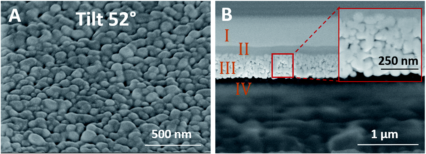 | ||
| Fig. 5 (A) SEM micrograph with a tilt of 52°. (B) Cross section micrograph of sintered printed silver line upon exposure to 600 kGy (region III). Region I and II belong to Pt protective layers, and region IV is of the PEN substrate. | ||
In traditional printing and curing with electron beam, the reaction pathway in N2 or air atmosphere is fundamentally different. In ebeam curing, nitrogen is typically used as a blanketing gas upon oxygen inhibition, but for the sintering of silver particles it is not required. Since slight oxidation of the silver could occur, we evaluated the effect of nitrogen atmosphere. The results presented in Fig. 6 show that although the resistivities under air are at same order of magnitude as those in nitrogen, the results scattering for sintering under nitrogen were much narrower. This might be due to possible oxidation of silver under air. It should be mentioned that there are certainly more angles to explore on the effects of atmosphere on the sintering of Ag inks and removal of the stabilizing agents.
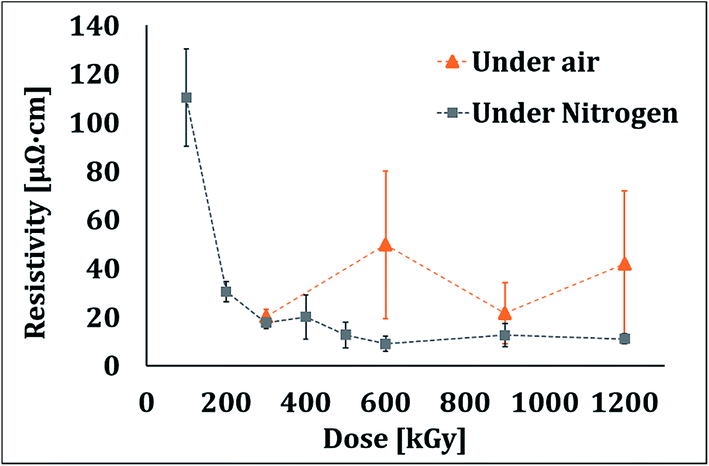 | ||
| Fig. 6 The resistivity of the silver patterns as a function of the doses at fixed voltage and conveyor speed (200 kV and 3 m min−1, respectively) for samples treated in nitrogen atmosphere and in air. | ||
For comparison with traditional thermal sintering, further experiments were done by printing the same patterns with same number of layers on PEN and drying for 10 min at 80 °C. The sintering was done in an oven under ambient conditions for 30 min at various temperatures (Fig. S2†). It was found that the samples sintered at 140 °C (7.8 ± 0.8 μΩ cm) and at 160 °C (2.0 ± 0.1 μΩ cm) are characterized by half and twice of the conductivity of ebeam-treated sample obtained at dose of 600 kGy, respectively. SEM micrographs of thermally sintered silver ink is presented in Fig. S3.†
Conclusions
In summary, to the best of our knowledge, this is the first report on applying ebeam for obtaining inkjet printed electrical conductors for printed electronics. Flexible printed electronics requires methods and materials, which are suitable for low cost substrates such as PEN and PET. The EB technique was found to enable printing of conductive patterns on PEN substrate without damaging it, at a conveyer speed, which is suitable for typical industrial roll-to-roll processes. Various beam parameters under both nitrogen and air were evaluated and electrical conductivity as high as 37% of bulk silver was obtained at optimal ebeam-sintering conditions. Thus, the application of high-power beams of accelerated electrons may be very effective for implementing in printed electronics for R2R processing.References
- H. W. Choi, T. Zhou, M. Singh and G. E. Jabbour, Nanoscale, 2015, 7, 3338 RSC.
- A. Kamyshny, J. Steinke and S. Magdassi, Open Appl. Phys. J., 2011, 4, 19 CrossRef CAS.
- J. Perelaer, P. J. Smith, D. Mager, D. Soltman, S. K. Volkman, V. Subramanian, J. G. Korvink and U. S. Schubert, J. Mater. Chem., 2010, 20, 8446 RSC.
- S.-P. Chen, H.-L. Chiu, P.-H. Wang and Y.-C. Liao, ECS J. Solid State Sci. Technol., 2015, 4, P3026 CrossRef CAS.
- S. Magdassi, The chemistry of inkjet inks, World scientific Singapore, 2010, vol. 20 Search PubMed.
- M. Singh, H. M. Haverinen, P. Dhagat and G. E. Jabbour, Adv. Mater., 2010, 22, 673 CrossRef CAS PubMed.
- G. Cummins and M. P. Desmulliez, Circuit World, 2012, 38, 193 CrossRef CAS.
- A. Teichler, J. Perelaer and U. S. Schubert, J. Mater. Chem. C, 2013, 1, 1910 RSC.
- H. Kang, R. Kitsomboonloha, J. Jang and V. Subramanian, Adv. Mater., 2012, 24, 3065 CrossRef CAS PubMed.
- B. Lee, S. Jeong, Y. Kim, I. Jeong, K. Woo and J. Moon, Met. Mater. Int., 2012, 18, 493 CrossRef CAS.
- J. Jo, J.-S. Yu, T.-M. Lee, D.-S. Kim and K.-Y. Kim, Mol. Cryst. Liq. Cryst., 2009, 514, 81 Search PubMed.
- B. W. An, K. Kim, M. Kim, S. Y. Kim, S. H. Hur and J. U. Park, Small, 2015, 11, 2263 CrossRef CAS PubMed.
- K. Kim, G. Kim, B. R. Lee, S. Ji, S.-Y. Kim, B. W. An, M. H. Song and J.-U. Park, Nanoscale, 2015, 7, 13410 RSC.
- S.-Y. Kim, K. Kim, Y. Hwang, J. Park, J. Jang, Y. Nam, Y. Kang, M. Kim, H. Park and Z. Lee, Nanoscale, 2016, 8, 17113 RSC.
- B. W. An, K. Kim, H. Lee, S. Y. Kim, Y. Shim, D. Y. Lee, J. Y. Song and J. U. Park, Adv. Mater., 2015, 27, 4322 CrossRef CAS PubMed.
- M. A. Skylar-Scott, S. Gunasekaran and J. A. Lewis, Proc. Natl. Acad. Sci. U. S. A., 2016, 201525131 Search PubMed.
- P. Karthik and S. P. Singh, RSC Adv., 2015, 5, 77760 RSC.
- K. Rajan, I. Roppolo, A. Chiappone, S. Bocchini, D. Perrone and A. Chiolerio, Nanotechnol., Sci. Appl., 2016, 9, 1 Search PubMed.
- S. Wünscher, R. Abbel, J. Perelaer and U. S. Schubert, J. Mater. Chem. C, 2014, 2, 10232 RSC.
- J. Niittynen, R. Abbel, M. Mäntysalo, J. Perelaer, U. S. Schubert and D. Lupo, Thin Solid Films, 2014, 556, 452 CrossRef CAS.
- V. Neronov, A. Voronin, M. Tatarintseva, T. Melekhova and V. Auslender, J. Less-Common Met., 1986, 117, 391 CrossRef CAS.
- M. Sigl, S. Lutzmann and M. Zäh, in Transient physical effects in electron beam sintering, Solid Freeform Fabrication Symposium Proceedings, Austin, TX, 2006, p. 397 Search PubMed.
- K. Makuuchi and S. Cheng, Radiation processing of polymer materials and its industrial applications, John Wiley & Sons, 2012 Search PubMed.
- K. Kanaya and S. Okayama, J. Phys. D: Appl. Phys., 1972, 5, 43 CAS.
- Y. Chen, R. E. Palmer and J. P. Wilcoxon, Langmuir, 2006, 22, 2851 CrossRef CAS PubMed.
- F. Salvat, J. M. Fernández-Varea and J. Sempau, in PENELOPE-2006: A code system for Monte Carlo simulation of electron and photon transport, Workshop proceedings, 2006 Search PubMed.
- W. K. Choi and S. Y. Baek, Materials, 2015, 8, 6498 CrossRef.
Footnote |
| † Electronic supplementary information (ESI) available: Graph of resistivity of silver patterns using conventional heating, and SEM micrographs. See DOI: 10.1039/c7ra00967d |
| This journal is © The Royal Society of Chemistry 2017 |