 Open Access Article
Creative Commons Attribution 3.0 Unported Licence
Enhancing performance of inverted planar perovskite solar cells by argon plasma post-treatment on PEDOT:PSS†
Miao Yu‡
a,
Xiaona Huang‡a,
Shuying Wang‡b,
Ben Chena,
Yang Zhanga,
Bo Chen*c,
Mingzhen Liu*a,
Wanli Zhanga and
Jie Xiong *a
*a
aState Key Laboratory of Electronic Thin Films and Integrated Devices, University of Electronic Science and Technology of China, Chengdu 610054, China. E-mail: Jiexiong@uestc.edu.cn; mingzhen.liu@uestc.edu.cn; Fax: +86 2883201232; Tel: +86 2883201231
bChengdu No. 7 High School (GaoxinCampus), Chengdu 610041, China
cInstitute of Microelectronics of Chinese Academy of Sciences, Beijing 100029, China. E-mail: b_chen@139.com
First published on 20th March 2017
Abstract
Interface engineering is an efficient method for improving the performance of inverted planar heterojunction perovskite solar cells (PSCs). In this paper, the PSCs were modified by introducing mild argon plasma post-treatment on poly(3,4-ethylenedioxythiophene):poly(styrene sulfonate) (PEDOT:PSS). The power conversion efficiency (PCE) was enhanced up to 12.17%, compared with 9.55% of the reference device without interlayer modification. We found that argon plasma treatment on the PEDOT:PSS layer effectively increases its conductivity due to the modification of the PSS ratio in the film. The argon plasma treatment time directly affects the surface morphologies and contact angles of the PEDOT:PSS layer and therefore optimises the uniformity of the PEDOT:PSS layer on the nanometer-scale. The improvement in the chemical compositions and film morphologies of PEDOT:PSS could be beneficial to enhancing the wettability and retarding the carrier recombination. The open-circuit voltage (Voc) and short circuit current density (Jsc) of PSCs based on the treated PEDOT:PSS were both improved, resulting in the enhancement of PCE.
1. Introduction
Organic–inorganic perovskite solar cells have attracted tremendous attention because of their high solar-to-electric power conversion efficiency (PCE) and low fabrication costs.1–4 The PCE of perovskite solar cells has been boosted from 3.8% (ref. 5) to certified 22.1% (ref. 6) in the past few years. As is known, the device performance is not only affected by the molecular properties of the cell components involved, but also dramatically dependent on the nature of the interfaces present. Hence, interface modification is an efficient method to improve the performance of perovskite solar cells.7 For inverted planar heterojunction perovskite solar cells, much effort has been made to modify the interface between the poly(3,4-ethylenedioxythiophene):poly(styrene sulfonate) (PEDOT:PSS) anode layer and perovskite active layer. For example, incorporating graphene oxide as a dual functional interface modifier can improve wettability and retard recombination in hybrid perovskite solar cells.8 Polar solvent (H2O, ethanol, and a mixture) treatment on PEDOT:PSS film was introduced to improve the conductivity but at the cost of a reduction of PCE of perovskite solar cells.9 The PCE of CuPc/fullerene-based solar cells could be significantly improved with an appropriate UV-ozone treatment on PEDOT:PSS.10 Recently, it was reported that PEDOT:PSS post-treated with oxygen plasma demonstrated improved conductivity, possibly resulting from a relatively increase of well-conducting PEDOT to less-conducting PSS ratio on the surface.11 Meanwhile, they found that the thickness of PEDOT:PSS layers was reduced with an etching rate of 5 nm min−1, confirming the removal of materials from the surface of PEDOT:PSS layer. Sometimes the effect of PEDOT:PSS film thickness variations on the device performance has to be considered especially for the pristine layer which has a relatively thin thickness. Atmospheric-pressure argon plasma etched PEDOT:PSS layer was used to improve the performance of organic thin-films solar cells as a hole-transport layer.12,13In this paper, a simple and effective method of argon plasma post-treatment on PEDOT:PSS was proposed to improve the performance of perovskite solar cells. The conductivity, component analysis, film thickness, surface morphology of the plasma-treated PEDOT:PSS films, as well as the wettability of the perovskite precursor solution deposited on these argon-treated PEDOT:PSS films were systematically investigated. Subsequently, perovskite solar cells based on argon plasma treated PEDOT:PSS films were fabricated and tested. The PCE of perovskite solar cells increased from 9.55% for the pristine PEDOT:PSS films based device to 9.62%, 12.17% and 10.34% for the argon plasma treated PEDOT:PSS film based devices by 1 min, 3 min and 5 min, respectively.
2. Experimental
2.1 Experimental materials
PEDOT:PSS (Clevios™ PVP. AI 4083) was purchased from Heraeus Materials Technology Shanghai Ltd. CH3NH3I was purchased from Deysol. Lead iodide (PbI2, 99%), anhydrous N,N-dimethylformamide (DMF, 99.8%) and anhydrous chlorobenzene (CB, 99.8%) were purchased from Sigma-Aldrich company. [6,6]-Phenyl-C61-butyric acid methyl ester (PC61BM, >99%) was purchased from Xi'an Polymer Light Technology Corp.2.2 PEDOT:PSS films fabrication and characterization
Firstly, indium tin oxide (ITO) coated on glass (1.5 × 1.5 cm2) was pre-cleaned by detergent, deionized water, acetone and ethanol in sequence. Then PEDOT:PSS films were deposited on the ITO coated glass by spin-coating the PEDOT:PSS solution at a speed of 5000 rpm. After heated at 150 °C on a hot plate for 10 min, the PEDOT:PSS films were mild argon plasma post-treated by plasma cleaner system with the type of PDC-36G under a base pressure of around 170 Pa for a certain time of several minutes from 0 to 5 min.When measuring the conductivity, the PEDOT:PSS films were directly deposited on the glass instead of ITO, and measured by Keithley B2902A system. Silver-indium was welded on the diagonal corners of each PEDOT:PSS film as the electrical contacts for the J–V characteristics measurement. The morphology of the films was observed by atomic force microscopic (AFM, SPI3800, Japan) and scanning electron microscope (SEM, JEOL, JSM-5900 LV). The wettability of CH3NH3PbI3 precursor solution (2.5 μL) and PEDOT:PSS film surface were measured by drop shape analyzer produced by KRUSS. X-Ray photoelectron spectroscopy (XPS) was carried out with an ESCALAB 250 electron spectrometer from the Chengdu Branch of the Chinese Academy of Sciences.
2.3 Device fabrication and characterization
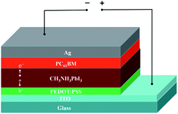
The schematic illustration of the inverted planar heterojunction perovskite solar cells with the structure of ITO/PEDOT:PSS/PVSK/PC61BM/Ag was shown in Fig. 1. The CH3NH3PbI3 perovskite active layer was deposited onto the as-prepared PEDOT:PSS layer by spin-coating CH3NH3PbI3 precursor solution (40 wt% in DMF) at 4000 rpm for 40 s. In order to improve the crystallization of perovskite active layer deposited by one-step solution method, 70 μL chlorobenzene was dropped quickly onto CH3NH3PbI3 wet film about 6 seconds after the beginning of spinning as reported in the literature.14 Then the films were annealed at 110 °C for 30 min inside the glove box filled with nitrogen. After that, a solution of PC61BM in chlorobenzene was spin-coated onto the perovskite film at 3000 rpm for 40 s. Finally, a 100 nm Ag layer was deposited by thermal evaporation process. The current density–voltage (J–V) measurement was carried out by Keithley model 2400 Source Meter under simulated AM 1.5G solar illumination (100 mW cm−2) generated by solar simulator (ABET Technologies, SUN 3000).3. Results and discussion
3.1 Effect of Ar plasma post-treatment on PEDOT:PSS
Fig. 2 and 3 show top-view SEM and cross-section SEM images of surface morphology of PEDOT:PSS films treated by the argon plasma as a function of treatment time, respectively. A nonuniform distribution of nanometer-scale islands with a diameter of around 50–100 nm was observed on the untreated PEDOT:PSS film. After the argon plasma treatment, the surface morphology of PEDOT:PSS film was observed that the density of islands increased but the size of the islands decreased. The bombardment of argon plasma resulted in a lot of etched small particles about 2–5 nm on the surface of the islands after 1 min treatment (Fig. 2b). As the treatment time increased, the density of nanometer-scale particles became higher (Fig. 2c). After 5 min treatment, the particles evolved into the uniformly distributed new islands about 15–20 nm which have replaced the pristine nonuniform big islands (Fig. 2d).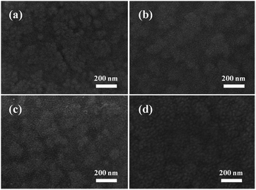 | ||
| Fig. 2 SEM images of PEDOT:PSS treated by argon plasma for different time: (a) untreated, (b) 1 min, (c) 3 min, (d) 5 min. | ||
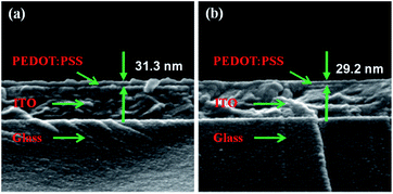 | ||
| Fig. 3 Comparison of the cross-section SEM images of PEDOT:PSS treated by argon plasma for different time: (a) untreated PEDOT:PSS, (b) 3 min. | ||
To investigate the effect induced by plasma post-treatment on the film thickness, a reference thickness was measured by Profilometer Tencor Alfa-step 500. The average thickness reduced from 107 nm to 84 nm after 30 min treatment, suggesting a removal rate of around 0.8 nm min−1. It was also confirmed by the cross-section SEM images as shown in Fig. 3. The thickness of untreated and 3 min treated films are 31.3 nm and 29.2 nm respectively, which is in accordance with the Profilometer measurements. The above results indicated that the plasma treatment process could remove materials from the surface of PEDOT:PSS layer quite slightly, which was slower than the removal rate of approximately 5 nm min−1 presented in the literature.11
The surface morphology of PEDOT:PSS films was also examined by AFM as shown in Fig. 4, which confirmed the observation from SEM. Initially, AFM image showed nanometer-scale islands with a size of approximately 100 nm (Fig. 4a) on the untreated PEDOT:PSS layer, suggesting a root-mean-square (RMS) of 1.12 nm. After 1 min treatment, small particles were found on the surface, which is ascribed to the removal of featureless top PSS chains from the surface15,16 (Fig. 4b) (RMS = 1.14 nm). With increased treatment time, the density of particles increased and the edge of the particles became shaper (Fig. 4c), and PEDOT:PSS surface showed more uniformed and more condensed grains. After 5 min treatment, the particles gradually connected to the adjacent ones and grown up to islands around 20 nm (RMS = 1.26 nm). It should be noticed that much rougher surface was found for argon plasma treated PEDOT:PSS films (Fig. 4b–d), among which 3 min treated PEDOT:PSS film formed roughest surface (RMS = 1.36 nm).
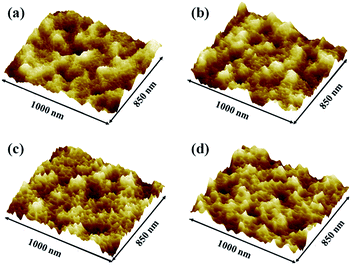 | ||
| Fig. 4 AFM surface images of PEDOT:PSS treated by argon plasma for different time: (a) untreated, (b) 1 min, (c) 3 min, (d) 5 min. | ||
To investigate the possible changes in the film conductivity, the conductivity of PEDOT:PSS film (σ) was calculated according to the following formulation:  . Rs and d represent the sheet resistance and the thickness of measured film, respectively. Rs was measured by a four-point probe method with a Keithley Instrument Model B2902A. To minimize the effect of the contact resistance between the PEDOT:PSS film and the probe, silver–indium layer was thermally deposited on the PEDOT:PSS surface as top electrode.
The conductivity is 12.8 mS cm−1 for pristine PEDOT:PSS film, and 14.3 mS cm−1, 15.5 mS cm−1, 17.9 mS cm−1 for the films treated by argon plasma for 1 min, 3 min and 5 min, respectively. The plasma-treated PEDOT:PSS layers exhibited enhanced conductivity, which may be attributed to the enlarged ratio of PEDOT to PSS. Normally, the PEDOT-to-PSS molar concentration ratio in films strongly affects the electrical conductivity and sheet resistance. The higher PEDOT concentration, the larger the electrical conductivity corresponding charge transporting layer.17
XPS spectra was measured to determine the surface component of PEDOT:PSS films modified by argon plasma post-treatment. Fig. 5 shows the S 2p spectra of pristine PEDOT:PSS films and treated films. Two binding energy components are observed at 164.0 and 168.2 eV, which are corresponding to PEDOT and PSS respectively.18,19 The S 2p contributing peaks at 163.9 and 165.3 eV result from the spin-split doublets of the sulfur atoms in PEDOT. On the other hand, the S signals from PSS are present at 166.5–171.0 eV because high-electronegative oxygen atoms are attached to sulfur fragments of PSS.20 The higher binding energy component of the S 2p peak at 169.2 eV (green line, Fig. 5) is associated with the SO3–H group of PSS, whereas the lower binding energy component of the S 2p peak at 168.1 eV (pink line, Fig. 5) corresponds to the SO3− group of PSS.21 With the increase of treatment time, the peak areas rate of PEDOT to PSS increased from 0.14 (untreated) to 0.27, 0.33, and 0.40, respectively, indicating that PEDOT-to-PSS molar concentration ratio are significantly enhanced during low energy argon plasma treatment, which is in good accordance with the aforementioned conductivity results. Unfortunately, the mechanism of the increasing PEDOT-to-PSS ratio by mild argon plasma treatment has not been fully understood yet. As descripted in the ref. 22 and 23, there is a layer of excess PSS with the thickness of approximately 32–43 Å surrounding the PEDOT–PSS grains at the surface. During argon plasma treatment, the excess PSS is easily removed away from the surface of the films, which is likely ascribed to the change of chemical compositions.
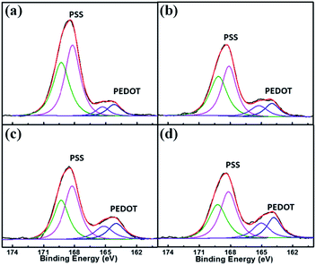 | ||
| Fig. 5 S (2p) core level spectrum for PEDOT:PSS films treated by argon plasma for different time: (a) untreated, (b) 1 min, (c) 3 min, (d) 5 min. | ||
The interfacial property of hole transport layers plays a critical role on the deposition of perovskite layers. To further study the surface wettability of PEDOT:PSS films, the contact angle measurements between the droplet of perovskite precursor solution and PEDOT:PSS films were executed at the same time. The difference between the argon plasma treated PEDOT:PSS films and un-treated PEDOT:PSS is compared. It is found that the contact angel of perovskite precursor solution on the untreated PEDOT:PSS films is 11.2°. After different argon plasma treatment time, the angle decreases to 8.9°, 7.2°, 7.1°, respectively.
It is suggested that the wettability can be significantly improved by argon plasma post-treatment, which can be mainly explained by the increased surface free energy.24 It also could be partially explained by the condensed particles or islands appeared on the treated surface which leads to a relatively higher specific surface area. Another reason is that the contamination or dust particle on surface of PEDOT:PSS may be removed by the plasma cleaning process. Fig. 6 shows images of final morphology by dropping 2.5 μL perovskite precursor solution on the PEDOT:PSS films after argon plasma treatment for 0 min, 1 min, 3 min, 5 min, respectively. It was seen that perovskite precursor solution is dispersed more easily on the argon plasma treated PEDOT:PSS films. Meantime, the surface wettability of treated PEDOT:PSS films and perovskite precursor solution is also found to be improved because of the bigger solution area in the pictures.
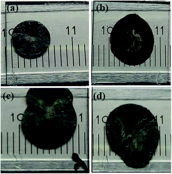 | ||
| Fig. 6 The morphology of perovskite precursor solution dropped on the PEDOT:PSS films for different time: (a) untreated PEDOT:PSS, (b) 1 min, (c) 3 min, (d) 5 min. | ||
3.2 The performance of the devices
Inverted planar heterojunction perovskite solar cells with the structure of ITO/PEDOT:PSS/CH3NH3PbI3/PC61BM/Ag were fabricated to study the influence of Ar plasma post-treatment on the cells' performance. The morphology and crystalline of the perovskite films on different treated PEDOT:PSS were characterized, as shown in Fig. S1.† It is found that the uniform grains could be obtained on the treated PEDOT:PSS, and the best morphology was grown on 3 min-treated one. The J–V characteristics and photovoltaic performance data corresponding to the power conversion efficiency (PCE) for various treating time were shown in Fig. 7.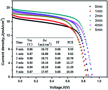 | ||
| Fig. 7 J–V curves and PV performance data of inverted planar PSCs based on PEDOT:PSS films treated by argon plasma as a function of treatment time. | ||
The pristine PEDOT:PSS films based device gave an open circuit voltage (Voc) of 0.86 V, a short circuit current density (Jsc) of 16.72 mA cm−2, a fill factor (FF) of 0.66 and a PCE of 9.65%. As the treatment time increased, the Voc increased to 0.87 V, 0.88 V, 0.92 V for 1 min, 2 min and 3 min, respectively. It reached a maximum of 0.94 V at 4 min, and then dropped down to 0.87 V at 5 min. Compared with the untreated PEDOT:PSS film based device, the Jsc increased from 16.72 mA cm−2 to 19.14 mA cm−2 excitingly, corresponding to the 3 min treatment. On the contrary, the argon plasma treatment has less influence on the value of FF except for 3 min treatment. Compared with the untreated PEDOT:PSS film based device, the PCE increased from 9.55% to 9.62%, 10.78%, 12.17%. Therefore, it indicates that an appropriate treating with argon plasma can effectively improve the performance of PSCs, which can be attributed to the enhanced Voc and Jsc.
The Jsc is found to be improved markedly by argon plasma post-treating on the surface of PEDOT:PSS films, which is attributed to an enhanced charge collection efficiency resulting from improved wettability between the perovskite layer and PEDOT:PSS layer.8 A higher conductivity caused by the removal of PSS concentration from XPS analysis may contribute to the improved Jsc. The significantly increased value of Voc could be explained by the changing of HOMO and LUMO band gap level presented by Attri, et al.,25 which leads to a restrained charge recombination. It should be noticed that, the devices based on PEDOT:PSS layer treated by 4 min and 5 min exhibit reduced efficiency of 11.29% and 10.34%, which are still higher than the efficiency of devices based on pristine PEDOT:PSS layer. In order to study the repeatability, 5 series of experiments at the same conditions have been executed, and the results showed that argon plasma post-treatment on PEDOT:PSS could effectively enhance the performance of inverted planar heterojunction perovskite solar cells, even though a certain fluctuation is presented, as shown in Fig. S2.†
4. Conclusions
In summary, we have systematically studied the influence of mild argon plasma post-treatment on the properties of the PEDOT:PSS films, the subsequent interface wettability between perovskite and PEDOT:PSS films, as well as the PSCs performance. XPS analysis confirmed that PSS component was partially removed, leading to an enhanced conductivity of a PEDOT-rich surface. SEM and AFM analysis revealed that argon plasma treated PEDOT:PSS surface appeared uniformly distributed islands with increasing surface roughness and consequently led to better wettability interface between perovskite film and PEDOT:PSS films. Although the PEDOT to PSS molar concentration ratio and surface morphology were modified, and the layer thickness was found to decrease slightly (0.8 nm min−1) for those plasma-treated PEDOT:PSS layers, which was evidenced by cross sectional SEM images and profilometer measurements. PSCs based on argon plasma treated PEDOT:PSS films were fabricated, and corresponding efficiency of PSCs remarkably increased from 9.55% for the pristine PEDOT:PSS films based device to 12.17% for the 3 min-treated PEDOT:PSS film. We believe that this method may be beneficial for enhancing the efficiency of all PSCs.Acknowledgements
This work was financially supported by National Key Basic Research Program of China (2014CB931702), NSFC (91421110 and 61604032), Sichuan Provincial Fund for Distinguished Young Academic and Technology Leaders (2014JQ0011). M. Y., X. H. and S. W. contributed equally to this work.References
- J. J. Nam, J. Noh, W. S. Yang, Y. C. Kim, S. Ryu, J. Seo and S. I. Seok, Nature, 2015, 517, 476–480 CrossRef PubMed.
- X. Li, D. Bi, C. Yi, J. Decoppet, J. Lou, S. M. Zakeeruddin, A. Hagfeldt and M. Grätzel, Science, 2016, 353, 58–62 CrossRef CAS PubMed.
- D. P. McMeekin, G. Sadoughi, W. Rehman, G. E. Eperon, M. Saliba, M. T. Hörantner, A. Haghighirad, N. Sakai, L. Korte, B. Rech, M. B. Johnston, L. M. Herz and H. J. Snaith, Science, 2016, 351, 151–155 CrossRef CAS PubMed.
- M. A. Green, A. Ho-Baillie and H. J. Snaith, Nat. Photonics, 2014, 8, 506–514 CrossRef CAS.
- A. Kojima, K. Teshima, Y. Shirai and T. Miyasaka, J. Am. Chem. Soc., 2009, 131, 6050–6051 CrossRef CAS PubMed.
- http://www.nrel.gov/ncpv/images/efficiency_chart.jpg.
- L. Jiang, S. Cong, Y. Lou, Q. Yi, J. Zhu, H. Ma and G. Zou, J. Mater. Chem. A, 2016, 4, 217 CAS.
- W. Li, H. Dong, X. Guo, N. Li, J. Li, G. Niu and L. Wang, J. Mater. Chem. A, 2014, 2, 20105–20111 CAS.
- X. Li, L. Zhang, F. Tang, Z. Bao, J. Lin, Y. Li, L. Chen and C. Ma, RSC Adv., 2016, 6, 24501–24507 RSC.
- Z. Su, L. Wang, Y. Li, H. Zhao, B. Chu and W. Li, Nanoscale Res. Lett., 2012, 7, 465 CrossRef PubMed.
- Y. Zhou, Y. Yuan, J. Lian, J. Zhang, H. Pang, L. Cao and X. Zhou, Chem. Phys. Lett., 2006, 427, 394–398 CrossRef CAS.
- T. Ino, T. Hayashi, K. Ueno and H. Shirai, Thin Solid Films, 2011, 519, 6834–6839 CrossRef CAS.
- T. Ino, T. Hayashi, T. Fukuda, K. Ueno and H. Shirai, J. Nanosci. Nanotechnol., 2011, 11, 8035–8039 CrossRef CAS PubMed.
- M. Xiao, F. Huang, W. Huang, Y. Dkhissi, Y. Zhu, J. Etheridge, A. Gray-Weale, U. Bach and Y. Cheng, Angew. Chem., Int. Ed., 2014, 53, 9898–9903 CrossRef CAS PubMed.
- J. Ouyang, Q. Xu, C. W. Chu, Y. Yang, G. Li and J. Shinar, Polymer, 2004, 45, 8443–8450 CrossRef CAS.
- J. S. Yeo, J. M. Yun, D. Y. Kim, S. Park, S. S. Kim, M. H. Yoon, T. W. Kim and S. I. Na, ACS Appl. Mater. Interfaces, 2012, 4, 2551–2560 CAS.
- I. Tomohisa, H. Tatsuya, U. Keiji and S. Hajime, Thin Solid Films, 2011, 519, 6834–6839 CrossRef.
- S. A. Spanninga, D. C. Martin and Z. Chen, J. Phys. Chem. C, 2010, 114, 14992–14997 CAS.
- J. Wang, R. S. Karmakar, Y. Lu, M. Wu and K. Wei, J. Phys. Chem. C, 2016, 120, 25977–25984 CAS.
- X. Crispin, S. Marciniak, W. Osikowicz, G. Zotti, A. W. Denier van der Gon, F. Louwet, M. Fahlman, L. Groenendaal, F. De Schryver and W. R. Salaneck, J. Polym. Sci., Part B: Polym. Phys., 2003, 41, 2561–2583 CrossRef CAS.
- G. Greczynski, T. Kugler and W. R. Salaneck, Thin Solid Films, 1999, 354, 129–135 CrossRef CAS.
- S. K. M. Jönsson, J. Birgerson, X. Crispin, G. Greczynski, W. Osikowicz, A. W. Denier van der Gon, W. R. Salaneck and M. Fahlman, Synth. Met., 2003, 139, 1–10 CrossRef.
- G. Greczynski, T. Kugler, M. Keil, W. Osikowicz, M. Fahlman and W. R. Salaneck, J. Electron Spectrosc. Relat. Phenom., 2001, 121, 1–17 CrossRef CAS.
- B. D. Beake, J. S. G. Ling and G. J. Leggett, J. Mater. Chem., 1998, 8, 2845–2854 RSC.
- P. Attri, V. Bharti, Y. S. Kim, J. Gaur, S. Chand, G. Kwon, S. Lee, W. Lee, E. H. Choi and I. T. Kim, Phys. Chem. Chem. Phys., 2014, 16, 27043–27052 RSC.
Footnotes |
| † Electronic supplementary information (ESI) available. See DOI: 10.1039/c7ra01718a |
| ‡ These authors contribute equally to this work. |
| This journal is © The Royal Society of Chemistry 2017 |

