 Open Access Article
Benchmark characterization of the thermoelectric properties of individual single-crystalline CdS nanowires by a H-type sensor†
Haidong Wang‡
 a,
Dingshan Zheng‡b,
Xing Zhang*c,
Hiroshi Takamatsu
 *a and
Weida Hu*b
aDepartment of Mechanical Engineering, Kyushu University, Fukuoka 819-0395, Japan. E-mail: takamatsu@mech.kyushu-u.ac.jp
bNational Lab for Infrared Physics, Shanghai Institute of Technical Physics, Chinese Academy of Sciences, Shanghai 200083, People's Republic of China. E-mail: wdhu@mail.sitp.ac.cn
cDepartment of Engineering Mechanics, Tsinghua University, Beijing 100084, People's Republic of China. E-mail: x-zhang@tsinghua.edu.cn
First published on 10th May 2017
Abstract
A precision H-type sensor method has been developed to measure the thermoelectric performance of individual single-crystalline CdS nanowires for the first time. A nanomanipulation probe was used to directly pick up an individual nanowire from the array and place it on the sensor. Our method is generally applicable to any nanowire synthesized in either array or powder form. By simply changing the external electrical circuits, the Seebeck coefficient, thermal conductivity, and electrical conductivity have been measured on the same nanowire sample to ensure high accuracy and reliability. CdS nanowires have a large Seebeck coefficient over 300 μV K−1 due to their wide band gap, while their thermal conductivity is only one-tenth of that of the bulk material owing to the significant phonon-surface scattering. The figure of merit, ZT, of the CdS nanowire is 0.01 at 320 K, which is larger by two orders of magnitude than the value for a Bi2S3 nanowire, showing a trend of rapid increase above 300 K.
1. Introduction
The rapidly increasing global demand for clean energy harvesting has led to an intense interest in thermoelectric materials that interconvert heat and electrical energy without the use of a heat engine or any moving parts.1–3 However, applications of thermoelectrics are still quite limited due to their low energy conversion efficiency.4,5 According to the dimensionless figure of merit of thermoelectric materials, ZT = S2σT/λ, where S, T, σ, and λ are the Seebeck coefficient, temperature, electrical conductivity, and thermal conductivity, respectively, a high thermoelectric efficiency can be achieved for a material with large S, high σ, and low λ. However, maximizing ZT is quite challenging because S, σ, and λ are coupled to each other so that an increase in one parameter often has an adverse effect on another parameter.4,6 In recent years, a significant breakthrough has been made in maximizing ZT by reducing the geometry of the sample from three-dimensional bulk structures to one-dimensional nanowires.7–9 Meanwhile, a variety of nanostructures such as superlattices,9 nanocomposites,10 and quantum dots11 have been created to increase ZT. The physical mechanisms can be understood based on two features. First, low-dimensional materials exhibit sharp peaks in the density of electronic states, indicating high thermopower.12–14 Second, the characteristic size of a low-dimensional material can be one or more orders of magnitude smaller than the mean free path of the phonons but is larger than that of the electrons and holes.7 Because phonons are the main heat carriers for most semiconductors, it is possible to reduce the thermal conductivity of the nanostructured system while preserving its bulk-like electronic structures.7Evaluation of the thermoelectric performance of an individual nanowire is important and essential for understanding the basic mechanisms and for the development of efficient thermoelectric devices. However, this is quite challenging because of the two following problems: (1) the thermoelectric properties of a nanowire are highly sensitive to its geometric size, crystalline structure, doping level, etc., with significant differences between the individual nanomaterials.15 The best strategy is to measure all three parameters involved in the ZT formula, namely the Seebeck coefficient, and electrical and thermal conductivities, using the same individual nanowire. Unfortunately, currently the method that meets this purpose is quite limited.6,15 (2) Sample preparation is difficult for the chemical vapor deposition (CVD) grown nanowire arrays. The nanowires in arrays cannot be separated and picked up by dispersing the samples on a copper grid. The nanowires are easily contaminated or damaged during the common ultrasonic dispersion process. It is therefore considerably difficult to suspend an individual nanowire for characterization of its thermoelectric parameters.
The method that has a potential to be used for measuring the thermoelectric properties of individual nanowire is only that uses suspended microdevices.16,17 While the four-terminal sensing technique greatly improves the measurement accuracy, the micro-fabrication process is quite complicated. In the previous work, we used a T-type sensor method to measure the thermoelectric properties of an individual Bi2S3 nanowire.15 The length, width, and thickness of the suspended nanofilm sensor were about 10 μm, 600 nm, and 40 nm, respectively, much smaller than the geometric size of the commonly used microdevices. This was the reason why the suspended nanofilm sensor had an ultra-high thermal sensitivity. For measuring the thermoelectric power, however, two sensors that respectively work as a Joule heater and a thermometer are needed.6 The T-type method had only one sensor and thus it made us use a complex AC heating/DC detecting scheme.15 In addition, our previous method is not applicable to nanowires grown in arrays, but only to those in the powder form.
In this report, we have developed the method from the T-type sensor to the H-type sensor, where a nanowire sample bridges two suspended nanofilm sensors, forming a letter “H”. The measurement accuracy and reliability have been much improved. Using the H-type sensor, the thermoelectric performance of an individual single-crystalline cadmium sulfide (CdS) nanowire is reported for the first time. CdS nanowires have attracted intense attention for use in transistors, solar cells, photo detectors, light-emitting diodes, thermoelectric materials, and other applications because of their direct wide band gap of 2.4 eV.18–20 However, to our knowledge, no thermoelectric properties has been reported on the CdS nanowires. Here, we picked up a single CdS nanowire directly from the arrays using a nanomanipulation probe, and measured the intrinsic properties of as-grown CdS nanowire without contamination or damage.
2. Experiment
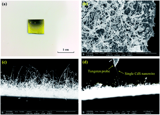
High quality single-crystalline CdS nanowire arrays were synthesized on a silicon substrate using the solid-source catalytic CVD method.21 More details about the synthesis of the CdS nanowires can be found in the ESI.† The optical and scanning electron microscope (SEM) images of the CdS nanowire arrays are shown in Fig. 1.By using different synthesis methods, semiconductor nanowires can be prepared in different forms such as powders, bundles, and arrays. To prepare the nanowires in the powder form, an ultrasonic dispersion method is usually used to separate a single nanowire on a copper grid. However, this method is not applicable for the nanowire arrays because the nanowire can be easily contaminated or damaged during the dispersion process. Here we successfully picked up an individual CdS nanowire from the arrays by using a microprobe as shown in Fig. 1(d). The nanowire was attached to the probe tip by the Coulomb force. This is a direct and non-destructive method that can be applied to any semiconductor nanowire array. Additional SEM images are presented in the ESI.†
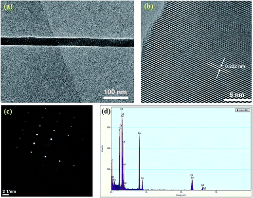
Fig. 2 shows the high-resolution transmission electron microscope (TEM) image, selected area electron diffraction (SAED) pattern, and energy dispersive X-ray (EDX) spectrum of the prepared CdS nanowire. The results clearly confirm the pure Cd and S chemical composition and the high quality single-crystalline structure. The observed lattice spacing is 0.322 nm, corresponding to the (002) plane. In the nanowire length direction vertical to the (002) plane, the layered crystal structure suppresses the heat conduction and leads to lower thermal conductivity. In contrast to the bulk material, the phonon scattering at the surface of the nanowire is greatly enhanced and is expected to significantly decrease the thermal conductivity.
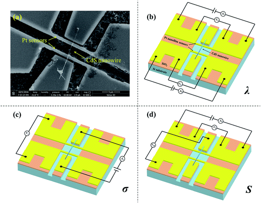
Fig. 3(a) shows the top SEM image of the suspended H-type sensor with the CdS nanowire. In the beginning, two nanofilm sensors (8 nm Ti/40 nm Pt) and an electrode pad were fabricated by using the standard electron beam lithography and physical vapor deposition methods. Then, the sensors were completely suspended after the removal of the SiO2 layer by buffered hydrofluoric acid and etching of the silicon by CF4 plasma. The etched depth was about 1.2 μm. Additional SEM images and details regarding the fabrication process can be found in the ESI.†
Next, we picked up an individual CdS nanowire (Fig. 1(d)) and placed it on the H-type sensor using a tungsten microprobe installed on a nanomanipulator from Kleindiek Nanotechnik. To reduce the electrical and thermal contact resistances between the nanowire and the sensor/electrode pad, Pt was deposited at four contact points using the electron beam induced deposition (EBID) method. All nanomanipulations, EBID processing, and thermoelectric measurements were carried out in a FEI Versa 3D™ dual-beam system (see ESI†).
Fig. 3(b–d) show three measurement schemes for the thermal conductivity λ, electrical conductivity σ, and Seebeck coefficient S of the same nanowire, respectively. In the λ measurement, two sensors were used as the Joule heater and the precise resistance thermometer, respectively. The electrical resistance of each sensor was measured by using two high-precision digital multimeters (Keithley 2002). The temperature rise of the sensor was linearly proportional to its resistance change. The temperature coefficient of the resistance and the thermal conductivity of the sensor were carefully calibrated beforehand. A detailed description of the calibration process can be found in ref. 22. In the experiment, a relatively large temperature rise (∼18 K) was generated at the sensor used as the heater. Due to the heat conduction through the nanowire, a small temperature rise was measured at the other sensor that was larger for the nanowires with the higher thermal conductivity values. λ of the individual CdS nanowire was extracted from the results of 2D thermal analysis (see the ESI†). In contrast to our previous T-type method, the H-type sensor shows a much higher thermal sensitivity because the temperature response of one sensor can be detected simultaneously with the electrical heating of the other sensor. Meanwhile, the estimated temperature resolution of the nanofilm sensor was less than 0.01 K.23 The H-type sensor provides a suitable approach for the measurement of a thermoelectric nanomaterial with a low thermal conductivity.
In the σ measurement, the four-terminal sensing technique was applied to the suspended nanowire. A current As was fed to the nanowire sample through two small electrode pads in the middle (Fig. 3(c)) and two sensors were connected to the multimeter for measuring the voltage drop Vs across the sample. Then, the electrical conductivity was determined as σ = 4AsL/(Vsπd2), where L = 3.05 μm and d = 125 nm were respectively the length and diameter of the nanowire obtained from the SEM image.
In the S measurement, one sensor was heated by an electrical current, and the temperature rise ΔT was measured through the resistance change of the sensor. Due to the temperature difference across the nanowire, a thermoelectric potential Vtp was generated in the CdS nanowire and was measured by a high-precision multimeter (Fig. 3(d)). The Seebeck coefficient was determined as S = |Vtp/ΔT|. All measurements were carried out in high vacuum (<10−4 Pa). The heat losses from the nanowire and the sensor to the environment through the interactions with the rarefied gas or thermal radiation can be safely neglected.15 By simply changing the measurement schemes, all three thermoelectric parameters can be measured in situ on the same nanowire sample, greatly improving the accuracy and reliability of the experimental data. The detailed uncertainty analysis for the thermal conductivity, electrical conductivity and Seebeck coefficient is given in the ESI.†
3. Results and discussion
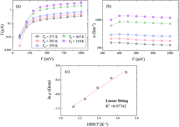
Fig. 4 shows the results of the electrical measurement of CdS nanowire.Our long-term goal is to fabricate efficient thermoelectric devices at room temperature. The temperature range of current work is from 0 °C to 46 °C, with the temperature controlled using a Peltier heating/cooling stage installed inside the high vacuum chamber. As illustrated in Fig. 4, the current of nanowire has a linear relationship with the bias-voltage after 500 mV. The electrical resistance of nanowire was calculated from the I–V curve from 500 mV to 1000 mV. A negative temperature dependence of the resistivity of CdS nanowire is found in Fig. 4(c), which indicates that the CdS nanowire exhibits a typical semiconductor electrical behavior. The measured resistivity obeys the standard Arrhenius relation:15
 | (1) |
Based on the result shown in Fig. 4, the charge mobility of the CdS nanowire was calculated using the following formula:24
 | (2) |
The measured thermal conductivities of the individual CdS nanowire and some other thermoelectric nanowires have been summarized in the Fig. 5.6,7,15–17,27,28 Our experimental result is in good agreement with the data measured using the optical Raman method (red line in Fig. 5).28 Due to the significant phonon-surface scattering effect, the thermal conductivity of CdS nanowire is only about one-tenth of that for the bulk material.29 With the rapid development of measurement techniques,30–32 this dramatic reduction in the thermal conductivity of the nanowire is commonly observed in the semiconductor nanowires.6,7,15 As illustrated in Fig. 5, the thermal conductivities of the different types of semiconductor nanowires are in the 0–5 W m−1 K−1 range. For the nanowire with a smaller diameter, the thermal conductivity can be further suppressed. The thermal conductivity of the single-crystalline CdS nanowire is about twice as large as that of the Bi2S3, Ge and Bi nanowires, probably due to its perfect lattice structure and smaller impurity content (see Fig. 2). For a thinner nanowire with a higher doping concentration, the thermal conductivity could be decreased further.
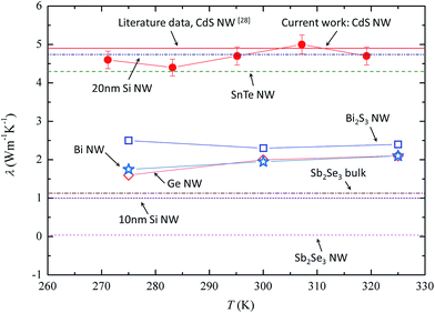 | ||
| Fig. 5 Measured thermal conductivity of CdS nanowire. Red circles are the measured thermal conductivity values of the single-crystalline CdS nanowire with 5% uncertainty. The red line is the experimental data from literature.28 In addition, the data reported for some other thermoelectric nanowires are also shown in the figure: Si (NW) nanowire with 10 or 20 nm diameter,7 SnTe nanowire,6 Bi2S3 nanowire,15 Sb2Se3 nanowire and bulk,27 Bi nanowire17 and Ge nanowire.16 | ||
Fig. 6 shows the measured ZT and Seebeck coefficient of the single-crystalline CdS nanowire. The Seebeck coefficient of the CdS nanowire is almost constant within the 260–330 K temperature range. The ZT value of the CdS nanowire shows a significant increase with increasing temperature from 300 K to 320 K. This rapid increase in ZT is due to the significantly enhanced electrical conductivity. The CdS nanowire ZT is around 0.003 at 300 K, which is two orders of magnitude larger than that of the single-crystalline Bi2S3 nanowire,15 and one order of magnitude smaller than that of the SnTe nanowire.6
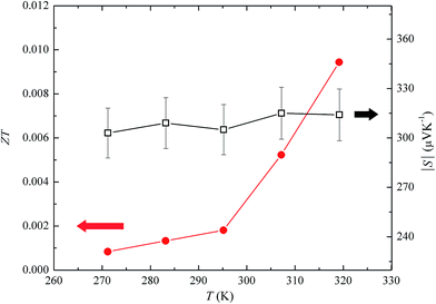 | ||
| Fig. 6 Figure of merit and Seebeck coefficient of the individual single-crystalline CdS nanowire as a function of temperature. | ||
Among three kinds of thermoelectric nanowires, Bi2S3, CdS and SnTe, the electrical conductivity varies from 100 S m−1 of Bi2S3 to 6 × 10⁵ S m−1 of SnTe at room temperature.6 The thermal conductivity of nanowire varies from 2.3 W m−1 K−1 of Bi2S3 to 4.7 W m−1 K−1 of CdS. The Seebeck coefficient varies from 50 μV K−1 of SnTe to 300 μV K−1 of CdS. It is clear that the electrical conductivity of nanowire plays the most important role in achieving high ZT values. Doping the semiconductor nanowire with other atoms could be an efficient way to increase ZT value, because the doped nanowire may have higher charge carrier concentration and lower thermal conductivity.
4. Conclusions
In this report, a novel H-type sensor was developed to measure the electrical conductivity, thermal conductivity and Seebeck coefficient of the same individual CdS nanowire. Compared to our previous T-type sensor or other microdevice methods, the H-type sensor method offers a high-precision four-terminal sensing measurement and ultra-high thermal sensitivity due to its suspended nanoscale structure. In this work, an individual nanowire was directly picked up from the arrays and connected to the sensor without contamination or damage caused by the conventional ultrasonic dispersion process. The CdS nanowire ZT value was about 0.003 at room temperature, smaller than the values obtained for the SnTe or Si nanowires. This was mostly due to the limited electrical conductivity.Author contributions
H. T. and X. Z. proposed and supervised the project. D. Z. and W. H. prepared the CdS nanowire samples and provided high-quality TEM images. H. W. designed and performed the experiments. H. W. wrote the manuscript. All the authors checked and revised the manuscript.Acknowledgements
The authors would like to thank Mr Tatsuya Ikuta, Dr Takanobu Fukunaga, Prof. Koji Takahashi, and Prof. Yasuyuki Takata for their help in fabricating the suspended H-type sensor and SEM operation. The work was supported by the JSPS KAKENHI Grant-in-Aid for Young Scientists A No. 17H04907 and National Natural Science Foundation of China Grant No. 51636002, 51327001 and 51356001.References
- G. J. Snyder and E. S. Toberer, Complex thermoelectric materials, Nat. Mater., 2008, 7, 105 CrossRef CAS PubMed.
- J. R. Sootsman, D. Y. Chung and M. G. Kanatzidis, New and old concepts in thermoelectric materials, Angew. Chem., Int. Ed., 2009, 48, 86168639 CrossRef PubMed.
- L. D. Zhao, S. H. Lo, Y. Zhang, H. Sun, G. Tan, C. Uher, C. Wolverton, V. P. Dravid and M. G. Kanatzidis, Ultralow thermal conductivity and high thermoelectric figure of merit in SnSe crystals, Nature, 2014, 508, 373 CrossRef CAS PubMed.
- J. F. Li, W. S. Liu, L. D. Zhao and M. Zhou, High-performance nanostructured thermoelectric materials, NPG Asia Mater., 2010, 2, 152 CrossRef.
- H. Bottner, G. Chen and R. Venkatasubramanian, Aspects of thin-film superlattice thermoelectric materials, devices, and applications, MRS Bull., 2006, 31, 211 CrossRef.
- E. Z. Xu, Z. Li, J. A. Martinez, N. Sinitsyn, H. Htoon, N. Li, B. Swartzentruber, J. Hollingsworth, J. Wang and S. X. Zhang, Diameter dependent thermoelectric properties of individual SnTe nanowires, Nanoscale, 2015, 7, 2869 RSC.
- A. I. Boukai, Y. Bunimovich, J. Tahir-Kheli, J. K. Yu, W. A. Goddard and J. R. Heath, Silicon nanowires as efficient thermoelectric materials, Science, 2008, 451, 168 CAS.
- A. I. Hochbaum, R. Chen, R. D. Delgado, W. Liang, E. C. Garnett, M. Najarian, A. Majumdar and P. Yang, Enhanced thermoelectric performance of rough silicon nanowires, Nature, 2008, 451, 163 CrossRef CAS PubMed.
- R. Venkatasubramanian, E. Siivola, T. Colpitts and B. O'Quinn, Thin-film thermoelectric devices with high room-temperature figures of merit, Nature, 2001, 413, 597 CrossRef CAS PubMed.
- B. Poudel, Q. Hao, Y. Ma, Y. Lan, A. Minnich, B. Yu, X. Yan, D. Wang, A. Muto, D. Vashaee, X. Chen, J. Liu, M. S. Dresselhaus, G. Chen and Z. Ren, High-Thermoelectric performance of nanostructured bismuth antimony telluride bulk alloys, Science, 2008, 320, 634 CrossRef CAS PubMed.
- T. C. Harman, P. J. Taylor, M. P. Walsh and B. E. LaForge, Quantum dot superlattice thermoelectric materials and devices, Science, 2002, 297, 2229 CrossRef CAS PubMed.
- L. D. Hicks and M. S. Dresselhaus, Thermoelectric figure of merit of a one dimensional conductor, Phys. Rev. B: Condens. Matter Mater. Phys., 1993, 47, 16631 CrossRef CAS.
- G. D. Mahan and J. O. Sofo, The best thermoelectric, Proc. Natl. Acad. Sci. U. S. A., 1996, 93, 7436 CrossRef CAS.
- T. E. Humphrey and H. Linke, Reversible thermoelectric nanomaterials, Phys. Rev. Lett., 2005, 94, 096601 CrossRef CAS PubMed.
- W. G. Ma, T. T. Miao, X. Zhang, K. Takahashi, T. Ikuta, B. P. Zhang and Z. H. Ge, A T-type method for characterization of the thermoelectric performance of an individual free-standing single crystal Bi2S3 nanowire, Nanoscale, 2016, 8, 2704 RSC.
- M. C. Wingert, Z. C. Y. Chen, E. Dechaumphai, J. Y. Moon, J. H. Kim, J. Xiang and R. K. Chen, Thermal conductivity of Ge and Ge–Si core–shell nanowires in the phonon confinement regime, Nano Lett., 2011, 11, 5507 CrossRef CAS PubMed.
- J. W. Roh, K. Hippalgaonkar, J. H. Ham, R. K. Chen, M. Z. Li, P. Ercius, A. Majumdar, W. C. Kim and W. Y. Lee, Observation of anisotropy in thermal conductivity of individual single-crystalline bismuth nanowires, ACS Nano, 2011, 5, 3954 CrossRef CAS PubMed.
- M. Y. Zhang, M. Wille, R. Röder, S. Heedt, L. B. Huang, Z. Zhu, S. Geburt, D. Grutzmacher, T. Schäpers, C. Ronning and J. G. Lu, Amphoteric nature of Sn in CdS nanowires, Nano Lett., 2014, 14, 518 CrossRef CAS PubMed.
- Y. Zhao, X. C. Yang, W. H. Huang, X. Zou and Z. G. Lu, Synthesis and optical properties of CdS nanowires by a simple chemical deposition, J. Mater. Sci., 2010, 45, 1803 CrossRef CAS.
- G. Y. Gou, G. Z. Dai, C. Qian, Y. F. Liu, Y. Fu, Z. Y. Tian, Y. K. He, L. G. Kong, J. L. Yang, J. Sun and Y. L. Gao, High-performance ultraviolet photodetectors based on CdS/CdS: SnS2 superlattice nanowires, Nanoscale, 2016, 8, 14580 RSC.
- D. S. Zheng, H. H. Fang, P. Wang, W. J. Luo, F. Gong, J. C. Ho, X. S. Chen, W. Lu, L. Liao, J. L. Wang and W. D. Hu, High-performance ferroelectric polymer side-gated CdS nanowire ultraviolet photodetectors, Adv. Funct. Mater., 2016, 26, 7690 CrossRef CAS.
- K. Nishimura, H. D. Wang, T. Fukunaga, K. Kurata and H. Takamatsu, Measurement of in-plane thermal and electrical conductivities of thin film using a micro-beam sensor: A feasibility study using gold film, Int. J. Heat Mass Transfer, 2016, 95, 727 CrossRef CAS.
- H. D. Wang, S. Q. Hu, K. Takahashi, X. Zhang, H. Takamatsu and J. Chen, Experimental study of thermal rectification in suspended monolayer graphene, Nat. Commun. Search PubMed , accepted..
- H. D. Wang, X. Zhang and H. Takamatsu, Ultraclean suspended monolayer graphene achieved by in situ current annealing, Nanotechnology, 2016, 28, 045706 CrossRef PubMed.
- K. W. Boer and K. Bogus, Electron mobility in CdS at high electric fields, Phys. Rev., 1968, 176, 899 CrossRef CAS.
- X. C. Yang, C. C. Xu and N. C. Giles, Intrinsic electron mobilities in CdSe, CdS, ZnO, and ZnS and their use in analysis of temperature-dependent Hall measurements, J. Appl. Phys., 2008, 104, 073727 CrossRef.
- T. Y. Ko, M. Shellaiah and K. W. Sun, Thermal and thermoelectric transport in highly resistive single Sb2Se3 nanowires and nanowire bundles, Sci. Rep., 2016, 6, 35086 CrossRef CAS PubMed.
- X. F. Liu, R. Wang, Y. P. Jiang, Q. Zhang, X. Y. Shan and X. H. Qiu, Thermal conductivity measurement of individual CdS nanowires using microphotoluminescence spectroscopy, J. Appl. Phys., 2010, 108, 054310 CrossRef.
- Cadmium Sulfide (CdS) semiconductors, Database from AZO Materials, 2013, http://www.azom.com/article.aspx?ArticleID=8407.
- J. H. Liu, H. D. Wang, W. G. Ma, X. Zhang and Y. Song, Simultaneous measurement of thermal conductivity and thermal contact resistance of individual carbon fibers using Raman spectroscopy, Rev. Sci. Instrum., 2013, 84, 044901 CrossRef PubMed.
- H. D. Wang, K. Kurata, T. Fukunaga, H. Takamatsu, X. Zhang, T. Ikuta, K. Takahashi, T. Nishiyama, H. Ago and Y. Takata, In-situ measurement of the heat transport in defect-engineered free-standing single-layer graphene, Sci. Rep., 2016, 6, 21823 CrossRef CAS PubMed.
- H. D. Wang, J. H. Liu, Z. Y. Guo, X. Zhang, R. F. Zhang, F. Wei and T. Y. Li, Thermal transport across the interface between a suspended single-walled carbon nanotube and air, Nanoscale Microscale Thermophys. Eng., 2013, 17, 349 CrossRef CAS.
Footnotes |
| † Electronic supplementary information (ESI) available: Synthesis method of CdS nanowires, SEM images of CdS nanowire and EBID process, temperature response of H-type sensor and 2D thermal analysis result. See DOI: 10.1039/c7ra02734f |
| ‡ Equally contributed authors. |
| This journal is © The Royal Society of Chemistry 2017 |

