
 Open Access Article
 This Open Access Article is licensed under a Creative Commons Attribution-Non Commercial 3.0 Unported Licence
Control of the compensating defects in Al-doped and Ga-doped ZnO nanocrystals for MIR plasmonics†
M. K. Hamza Tahaa,
O. Boisronb,
B. Canuta,
P. Melinonb,
J. Penuelasc,
M. Gendryc and
B. Masenelli *a
*a
aUniv. Lyon, INSA-Lyon, ECL, UCBL, CPE, CNRS, INL-UMR5270, F-69621, Villeurbanne, France. E-mail: bruno.masenelli@insa-lyon.fr; Tel: +33 4 72 43 74 72
bUniv. Lyon, Univ. Lyon 1, CNRS, ILM-UMR5306, F-69622, Villeurbanne, France
cUniv. Lyon, ECL, INSA-Lyon, UCBL, CPE, CNRS, INL-UMR5270, F-69134, Ecully, France
First published on 31st May 2017
Abstract
In degenerate semiconductor nanoparticles, the tuning range of the plasmon resonance is directly controlled by the electron gas concentration and thus by the dopant activation. Here, we investigate the improvement of the dopant activation in ZnO-based nanocrystals for mid IR plasmonics. For that purpose, we have synthesized Al-doped and Ga-doped ZnO nanocrystals in O-rich and O-poor environments. We show that the free carrier concentration can be doubled for the samples grown in an O-poor environment. Accordingly, the plasmon resonance shifts from 5 μm to 3.1 μm. In analogy with previous results from Ga-doped ZnO thin films, we discuss the effect of the possible reduction of the concentration of acceptor-like complexes such as AlZn–VZn and AlZn–Oi (resp. GaZn–VZn and GaZn–Oi) on the activation improvement. Besides, whether long or rapid, thermal annealing does not improve the compensation ratio. Consequently, the control of O content during synthesis remains the most valuable tool to achieve the highest dopant activation in doped ZnO nanocrystals.
1. Introduction
The research in the field of plasmonics is dominantly focused on the UV-visible and near IR ranges. Comparatively, research on mid infrared (MIR) plasmonics is emerging. Design and optimization of MIR materials and devices are yet a challenge. However, tuning the plasmon resonance to the MIR range would allow the design of label-free chemical sensors of high sensitivity since many chemical molecules (of pollutants for instance) exhibit vibrational modes in that range. Consequently, MIR plasmonic nanomaterials are key materials for Surface Enhanced IR Absorption (SEIRA) spectroscopy.1,2 Doping of metal oxide nanocrystals for infrared (IR) plasmonics has been recently investigated in order to tune the plasmon resonance and amplify the associated local electromagnetic field across the IR range.3–10 Varying the dopant concentration in degenerate metal oxide semiconductors can modulate the free electron density over one order of magnitude (from a few 1019 cm−3 to more than 1021 cm−3).10,11 Accordingly, the plasmon resonance wavelength can be tuned from about 1 μm to 5 μm. However, when the doping level reaches degeneracy, the activation of dopant is reduced, as is evidenced by Brouwer's diagram.12 Generally, much less than 1/2 of the dopant atoms introduced effectively contribute to the free electron gas. Typical values of the dopant activation usually range between 10% and 50%. This is particularly true for Ga and Al dopants in ZnO nanocrystals or for Sn in indium tin oxide (ITO) particles.13,14 The issue of incomplete dopant activation has been addressed first by groups working on transparent conductive oxide (TCO) thin films. The dopant efficiency is reduced because of the formation of compensating centers. For instance, in the case of Sn doped indium oxide,15 complexes between substitutional tin (SnIn) and oxygen interstitials (Oi) are increasingly stable and act as acceptor centers, hence compensating the n-doping of Sn. The same kind of mechanism has been evoked in Ga-doped ZnO thin films16 with the formation of GaZn–Oi and GaZn–VZn acceptor complexes. Because of the required presence of defects such as Zn vacancies (VZn) or O interstitials (Oi), the formation energy of these complexes depends on the amount of oxygen during the growth. Thus, in O-rich growth conditions, the presence of both VZn and Oi is expected to be favored and the formation energy of the GaZn–Oi and GaZn–VZn acceptor complexes is low. On the contrary, in O-poor growth conditions, the stabilization of the acceptor complexes is less likely. This mechanism has been evoked to explain the improved electric conductivity of TCO grown in O-poor conditions. It is thus appealing to study the impact of oxygen on the electronic and optical properties of MIR nanocrystals, and hence on the tuning of the plasmon resonance.In this work, we investigate the influence of oxygen pressure during the synthesis on the plasmon resonance in Al-doped (AZO) and Ga-doped (GZO) ZnO nanocrystals. We report on the physical synthesis of uncapped ZnO nanocrystals doped at 3% with either Al or Ga by an adiabatic plasma expansion in high vacuum. The doping level of 3% was chosen as an optimal compromise between an intense LSPR and a good reproducibility of the samples. Indeed, we have observed in a previous work17 that for doping levels lower than 6%, the nanocrystals are homogeneous in doping and thus are below the solubility limit of Al or Ga within our synthesis process while exhibiting clear and reproducible LSPR. Since the nanocrystals had uncapped surfaces, they tended to spontaneously self-organize through the oriented attachment (OA) process. Doped-ZnO nanocrystals have been synthesized in O-poor as well as in O-rich conditions. We have succeeded in modulating the plasmon resonance from 5 μm to about 3.1 μm by synthesizing the nanocrystals in an O-poor environment. Correspondingly, the resulting free carrier density has been increased significantly. We discuss about the possible relation between this increase in free carrier density and the concentration reduction of acceptor defects and complexes such as AlZn–Oi and AlZn–VZn (resp. GaZn–Oi and GaZn–VZn as seen in Ga-doped ZnO thin films). Next we investigate the impact of a post-deposition annealing to further improve the dopant activation. Contrary to what is observed for thin films, thermal treatment is detrimental to the plasmon of the nanocrystals, questioning the metastability of the dopants.
2. Methods
The nanocrystals have been synthesized by the low energy cluster beam deposition (LECBD) technique described in.17,18 A plasma is obtained from a target which is ablated using a pulsed (10 Hz repetition rate) doubled (532 nm; 100 mW) YAG: Nd laser. The 3% Al (Ga) doped ZnO pellet target consists of a mixture of ZnO and Al2O3 (Ga2O3) (99.999% pure each) microscopic powders sintered and annealed at 800 °C in air for 10 h. A constant flux of buffer gas is used to quench the plasma. The gas flux was a mixture of 75% He and 25% O2 for the AZO nanocrystals obtained in O-rich conditions. For the O-poor synthesis, no O2 gas was added to He. After the ablation of the target, the gas induces stabilization of nucleation embryos (dimers and trimers). Subsequently the mixture of the plasma species and buffer gas is expanded through a micrometer nozzle while leaving the nucleation chamber at 20 mbar and reaching the deposition chamber at 10−7 mbar. During this adiabatic expansion, atoms from the plasma aggregate according to an accretion process; at that point the formation of the clusters is achieved. The resulting nanocrystals forming a supersonic jet are deposited on silicon substrates or TEM grids. Despite their high velocity, the atomic kinetic energy in the nanocrystals is lower than the atomic binding energy. Therefore, the nanocrystals do not fragment during deposition. The films resulting from the deposition of the nanocrystals are typically several hundreds of nm thick and foam-like, with a porosity estimated to be about 70% according to the 3D percolation theory.The structure of the deposited nanocrystals was investigated by transmission electron microscopy (TEM) and X-ray diffraction (XRD). High resolution TEM images were acquired on a JEOL 2010F operating at 200 kV, equipped with a Gatan Orius 100 CCD camera. XRD diffractograms were acquired on a Rigaku Smartlab diffractometer using the Cu Kα1 radiation (λ = 1.54 Å), the incident beam was fixed at a grazing angle of 0.4° in order to increase the surface diffraction. The elemental composition of the whole nanocrystal films has been measured by Rutherford Backscattering Spectrometry (RBS) using a 4He++ ion beam accelerated at 5 MeV delivered by the van de Graaff accelerator of the Nuclear Physics Institute of Lyon (IPNL). A 13 keV resolution implanted junction, set at an angle of 172° with respect to the beam axis, has been used to detect the backscattered particles. Chemical states of the constituents have been analyzed by X-ray Photoelectron Spectroscopy (XPS), using an Al anode. The spectra have been calibrated by using the C1s level of adventitious carbon species as standard references with a nominal value of 285.0 eV. Eventually, the plasmon resonances have been probed by Fourier Transform Infrared Spectroscopy (FTIR) in the reflection mode.
3. Results
The LECBD technique has been previously used to synthesize undoped and Ga doped ZnO nanocrystals.17,18 As in these previous cases, the Al-doped and Ga-doped nanocrystals synthesized in both O-rich and O-poor environments are crystallized in the wurtzite structure. This is confirmed by TEM analysis in the high resolution mode and shown in Fig. 1. The average size distribution of the nanocrystals (estimated over 100 particles) is 5.6 ± 0.3 nm.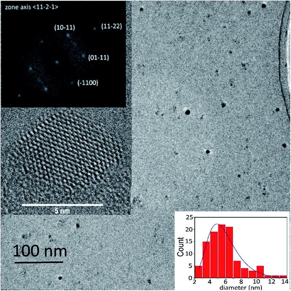 | ||
| Fig. 1 Low magnification TEM image of AZO nanocrystals. Inset: high resolution TEM image of an AZO nanocrystal, doped at 3% and the corresponding FFT, indicating the wurtzite structure of the nanocrystal. The size distribution of the nanocrystals is also shown (lower inset) revealing a mean size of 5.6 nm. The solid line is a fit to the data with a log-normal distribution, typical of the accretion process involved in the LECBD synthesis. | ||
Fig. 2 shows the XRD diffractograms of AZO nanocrystal films. The peaks correspond to the wurtzite structure with no additional peak indicating the absence of any other crystalline phase (see Fig. S2 of ESI† for large scan diffractogram). However, the average size of the crystalline domains, deduced using Scherrer's equation and assuming perfect crystals without defects, is 29 ± 2 nm for all samples. This discrepancy has already been pointed out and reported for pure ZnO18 and Ga doped ZnO nanocrystals17 produced by the LECBD technique. It results from the oriented attachment (OA) of the initial uncapped nanocrystals (see Fig. S3 of ESI†). The nanocrystals tend to reduce the surface energy of their facets through epitaxial attachment. The influence of the OA on MIR plasmon resonance has been studied intensively in.17 We have shown that it essentially leads to the inhomogeneous broadening of the plasmon resonance but has almost no effect on the dopant compensation. Moreover, the diffractograms do not show any shift of the peak positions. In AZO nanocrystals synthesized by wet chemical route, a slight increase of the peak position, corresponding to a small shrinkage of the lattice, has been reported.19 Al having an ionic radius (50 pm) smaller than that of Zn (74 pm), this shrinkage has been considered as a confirmation of the substitution of Zn with Al. If this statement holds, we can infer that, in our nanocrystals, not all the Al atoms are incorporated on substitutional sites. Nevertheless, the incorporation of Al (or Ga) in our nanocrystal films has been confirmed by RBS. The measured content of Al in AZO and Ga in GZO nanocrystals, whether obtained in O-rich or O-poor environment, is 3% in atomic concentration with respect to Zn.
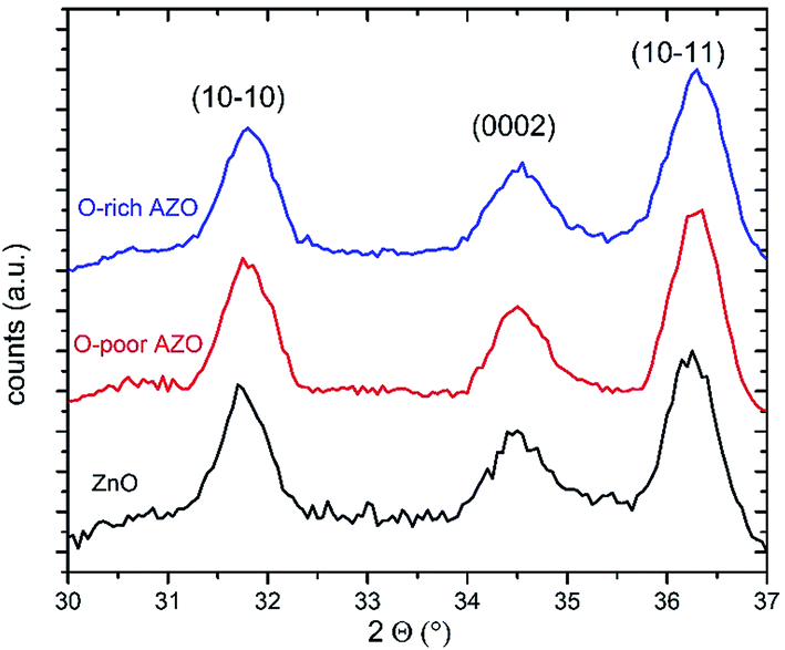 | ||
| Fig. 2 Diffractograms of the ZnO nanocrystal sample and of O-rich and O-poor AZO nanocrystal samples with 3% Al content. | ||
The effect of synthesizing nanocrystals in O-poor and O-rich environments on the IR plasmon properties of the resulting films was investigated by FTIR reflectance measurements. The plasmon peaks of the 3% AZO and GZO nanocrystals synthesized in O-rich and O-poor environments are shown in Fig. 3. As expected, the plasmon peaks are characterized by large broadening. This broadening is a common feature of doped nanocrystals.6,13,14,17 It is related to several distinct causes, such as the inherent plasmon damping (in Drude's model), which leads to the homogeneous broadening. It is also related to the inhomogeneity of the nanocrystal size and shape,20,21 the dopant segregation among the nanocrystals, the variation of the electron concentration between nanocrystals12 and the nanocrystal organization (oriented attachment). The sum of the optical responses of nanocrystals of different sizes, shapes and electron densities gives rise to a broad plasmon peak.
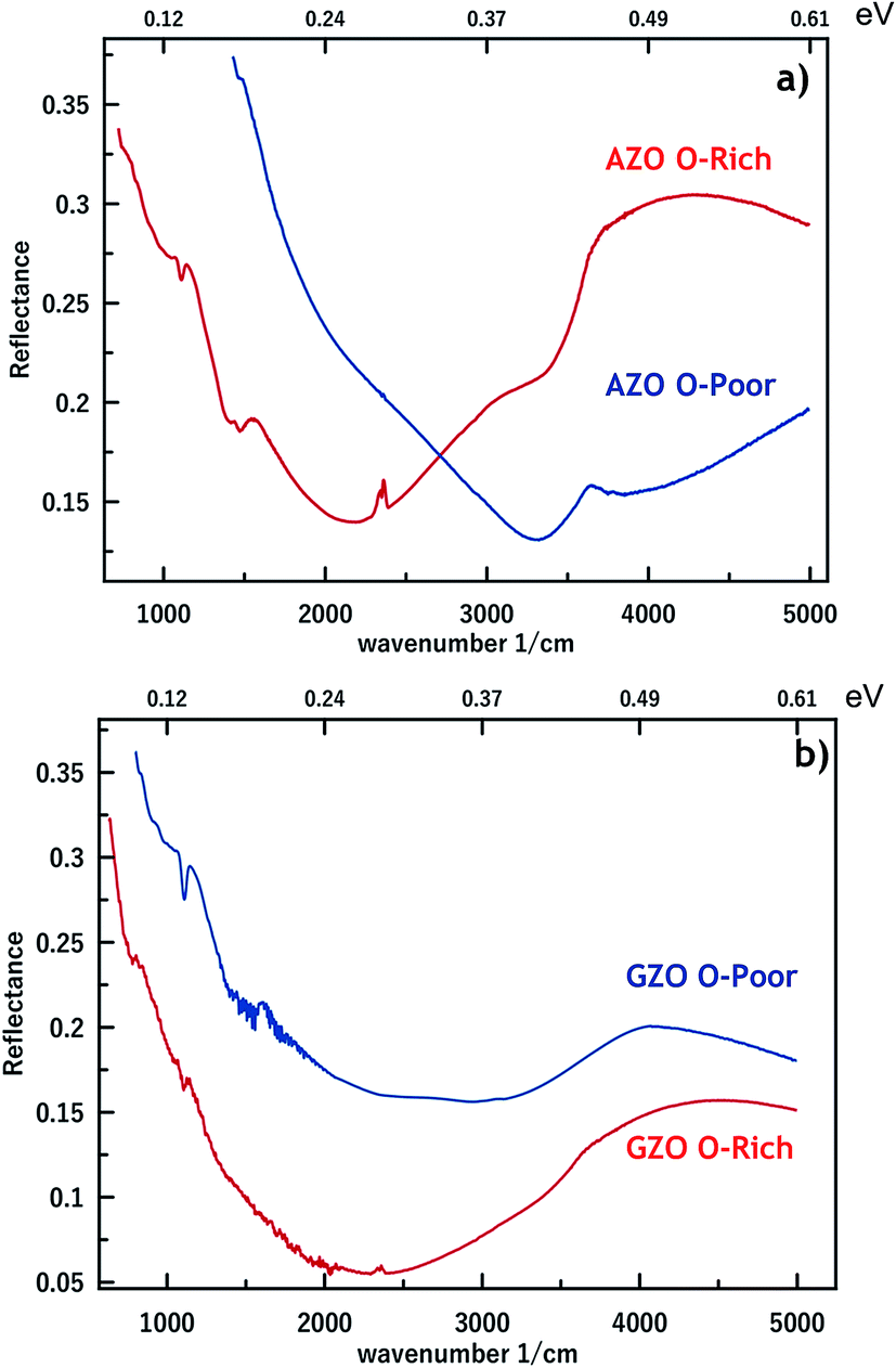 | ||
| Fig. 3 FTIR reflectance spectra of (a) AZO and (b) GZO nanocrystal films synthesized in oxygen rich (O-rich) and oxygen poor (O-poor) conditions deposited on Si substrates. | ||
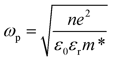
In Fig. 3a, we observe that the plasmon resonances of AZO nanocrystal films resulting from a synthesis in O-rich and O-poor environments peak at 2000 cm−1 (5 μm or 0.25 eV) and 3200 cm−1 (3.1 μm or 0.40 eV), respectively. For GZO nanocrystals (Fig. 3b), the shift is slightly lower, ranging from 2000 cm−1 (5 μm or 0.25 eV) to 2700 cm−1 (3.75 μm or 0.33 eV). From the observed plasmon resonances, we deduce the free electron density according to Drude's model. The frequency of the bulk plasmon resonance ωp is related to the electron density n through the following expression:
 | (1) |
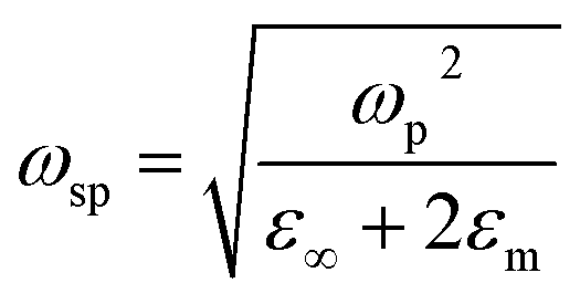 | (2) |
Synthesizing AZO or GZO nanocrystal films in O-poor conditions is conclusively beneficial for the improvement of the free electron density. This observation has been demonstrated for GZO16,22 or AZO23 thin films. As mentioned in the introduction, in the latter case, the improvement has been assigned to the reduced concentration of the GaZn–VZn or GaZn–Oi acceptor complexes. Demchenko et al.16 have computed the formation energy of these complexes and shown that in O-rich conditions, when the Fermi level is high, as in the case of degenerate ZnO, it is lower than that of the donor GaZn. Actually, the most stable and thus most likely complex is GaZn–VZn. In O-poor conditions, the formation energy of both complexes is higher by 6.70 eV making them less likely to exist. Hence, the compensating effect is reduced. This is a common feature in Al or Ga doped ZnO thin films. Moreover, other kinds of acceptor defects have been pointed out. At odd with the DFT calculations from Demchenko et al. which do not predict VZn as a stable defect, Look et al. have noticed that, in films grown with pulsed laser ablation, VZn can compensate partially the donors.24 Nevertheless, this study also points towards the role of Zn deficiencies, and thus indirectly to the O pressure during the growth, since a large O pressure is expected to favor the presence both VZn and Oi. In Ga-doped ZnO thin films, the compensation ratio was reduced from 90% to less than 30% (ref. 14) or set at 57% by controlling the synthesis ambient. In our AZO nanocrystal films the compensation ratio is reduced from 83% to 65%. Since we experience exactly the same behavior related to the O conditions of growth, we believe that in our system, acceptors either related to VZn or Oi are involved, possibly the GaZn–VZn or GaZn–Oi acceptor complexes.
In order to support this hypothesis, we have analyzed the chemical states of O within the nanocrystals by XPS. The O1s levels of O-rich and O-poor AZO nanocrystals are shown in Fig. 4. Both spectra show two distinct contributions labelled O1 and O2. The O1 contribution, peaking at 530.6 eV, is ascribed to O2− ions in a well-crystallized wurtzite environment, in accordance with ref. 25 and 26. The second contribution O2, peaking at 532 eV is assigned to O from hydroxide groups or to O in an O-deficient environment. O2 line is thus and indirect signature of O vacancies (VO). The ratio of the intensities of the O1 and O2 lines changes from 1.6 for the O-rich nanocrystals to 0.6 for the O-poor ones. The OH content being identical in both samples, the change of the O1/O2 ratio indicates the reduction of O content in the nanocrystals synthesized in O-poor conditions. Accordingly, the presence of Oi and VZn is expected to be drastically reduced, as is the presence of related compensating centers.
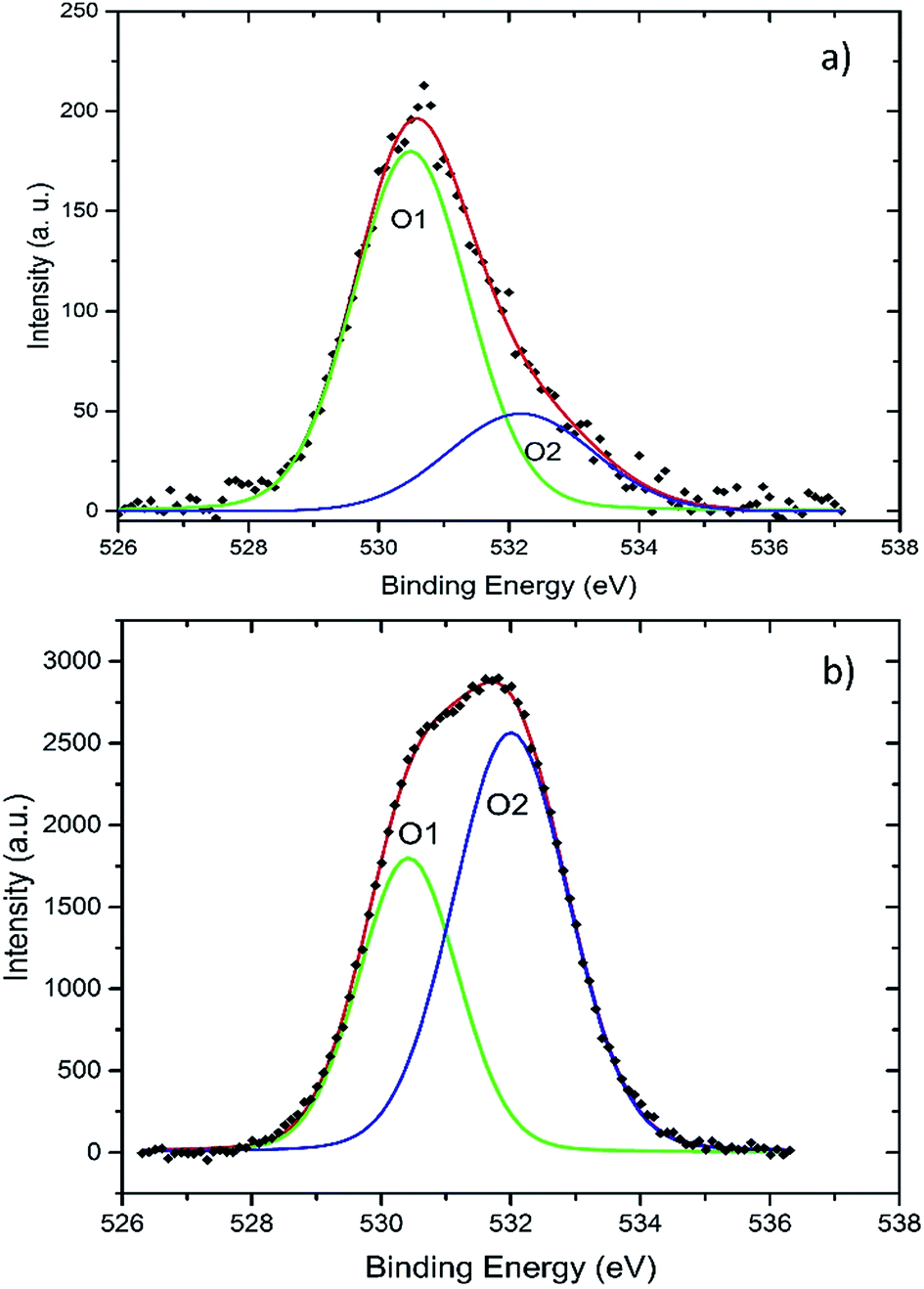 | ||
| Fig. 4 XPS spectra of the O1s level for 3% AZO nanocrystals synthesized in O-rich conditions (a) and O-poor conditions (b). The experiment results correspond to ♦ symbols. The O1 and O2 contributions are shown as the result of their sum (solid line). | ||
Even though we managed to reduce the acceptor complexes concentration, we note that our samples still have other compensating defects. Indeed, the presence of uncapped surfaces, of grain boundaries and twin boundaries resulting from the oriented attachment may play also a role. Embedding the AZO (or GZO) nanocrystals in a matrix leading to a clean and passivated surface of the nanocrystals might reduce significantly the acceptor-like defects (see27). Moreover, controlling the position of the donor centers among the nanocrystals could also be beneficial, as revealed by Milliron et al. for nanocrystals15 and by Look et al. for thin films.28 Eventually, we have to consider the possibility that the dopants do not go on the proper sites. In the drastically kinetic conditions of our growth process, we cannot discard that some Al or Ga atoms are incorporated on O sites (anti-sites) or interstitial sites. This would lead to metastable acceptor defects. As evidenced previously, the high resolution X-rays diffractograms of pure ZnO and 3% AZO nanocrystals (synthesized in O-rich or O-poor condition) do not show any shift of the peak positions. This may reveal that a significant part of the Al ions is not incorporated in Zn sites.
This observation has been made also for thin films and the latter are often subject to post-deposition annealing. Consequently, we have first annealed our 3% AZO O-rich nanocrystal films in air for 30 minutes at low temperature (50 °C) and high temperature (400 °C). In Fig. 5, we clearly observe that the low temperature annealing has no effect on the LSPR while the high temperature one leads to its complete disappearance. This is in fair agreement with results from Kortshagen et al.27 where the disappearance of the LSPR in AZO nanocrystals was observed after a 1 h annealing at 650 °C. Thus, instead of improving the activation of the dopants, it clearly shows that either the latter are in a metastable state or annealing induces additional compensating centers. Taking this metastability into account and considering that the diffusion length of Al in ZnO at high temperature can be as large as few nanometers, we next annealed the 3% AZO O-rich nanocrystal films by Rapid Thermal Annealing (RTA) in vacuum at moderate temperature (350 °C) for 1 or 2 minutes. This temperature was chosen from studies in the literature showing improvements of degenerate ZnO close to this value.29–32 The results are presented in Fig. 5b. Here again annealing leads to the annihilation of the LSPR. Our results emphasize a discrepancy between certain studies regarding degenerate ZnO thin films and our nanocrystals since in thin films a RTA has been shown to improve the dopant activation.16 However, for the sake of rigor, we mention that even in degenerate thin films, annealing at moderate temperature (ca. 350 °C) has been show to degrade the dopant concentration and thus the electron gas concentration.33 Actually, the annealing atmosphere matters. It seems that annealing in air, oxygen or nitrogen reduces the carrier concentration32,33 whereas annealing in reducing atmosphere seems to improve it.34–36 To further check the influence of the annealing atmosphere, we have repeated the RTA in a neutral ambient, Ar. The reduction of the electron gas concentration is still observed but to a lesser extent (see ESI S4†). Eventually, we have annealed an O-rich 3% doped AZO nanocrystal sample in H2 (400 °C, 30 min). The MIR reflectance spectrum, presented in (Fig. S5 of ESI†), does not show any LSPR anymore. This highlights that both mechanisms are involved. The addition of compensator centers is evidenced by the fact that the reduction of the LSPR is larger with an oxidizing ambient. On the other hand, when annealing in an inert atmosphere, the introduction of charged species is less likely. Eventually, the annealing in a reducing atmosphere should provide extra electrons to help saturating the electron traps. However, in the annealing conditions used here, this is not the case. The duration of the annealing seems to matter. The LSPR disappearance thus questions the metastability of the acceptors.
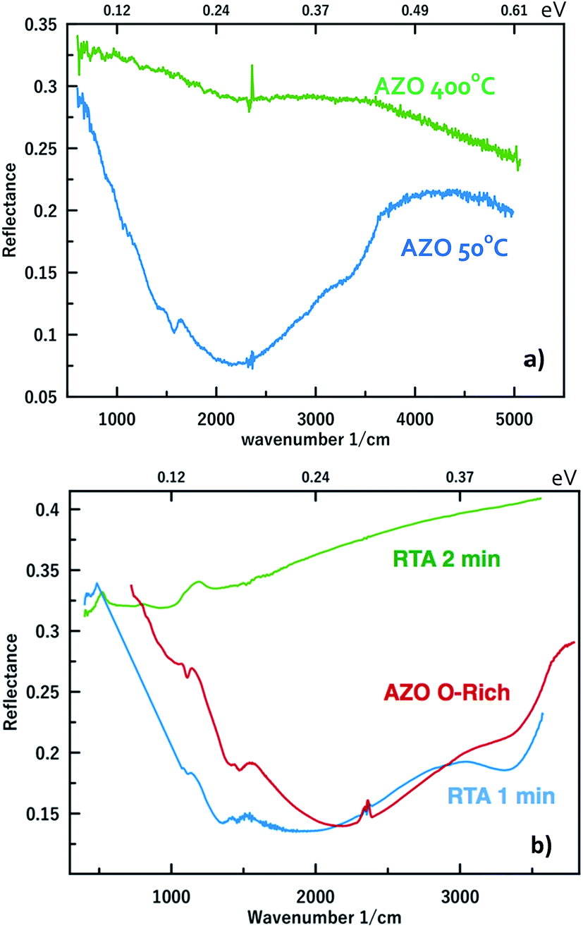 | ||
| Fig. 5 FTIR reflectance spectra of (a) 3% AZO nanocrystal films annealed in air at 50 °C and 400 °C for 30 minutes and (b) of 3% AZO nanocrystal films annealed by RTA at 350 °C for 1 mn and 2 mn. | ||
Another important point concerns the homogeneity of the compensation. We have no evidence about its possible variation from nanocrystal to nanocrystal but we can expect at least some stochastic variations. Since it has been shown that variations of the free electron density between different nanocrystals lead to an inhomogeneous broadening of the LSPR,13 it would be very interesting to measure the compensating ratio at the nanocrystal scale and see how it can be controlled in order to design nanocrystals with very sharp LSPR.
4. Conclusion
To conclude, we have investigated the improvement of dopant activation in ZnO nanocrystals for Mid IR plasmonics. First, the influence of the O amount during the growth on the LSPR of AZO and GZO nanocrystals has been studied. We have synthesized nanocrystal films either in O-rich or O-poor environment. While the Al (or Ga) content is not affected, the carrier density is doubled, varying from 2 × 1020 cm−3 for the O-rich synthesis to 4 × 1020 cm−3 for the O-poor one. Accordingly, the compensation ratio decreases from 83% to 65%. In analogy with previous calculations and observations on Ga-doped and Al-doped ZnO nanocrystal films, we propose that the increase in the carrier density is related to the concentration reduction of acceptor-like defects and complexes such as AlZn–VZn and AlZn–Oi. Despite the improvement of the compensating ratio the carrier density absolute value remains rather low, pointing to the presence of other compensating centers. Contrary to what has been observed for thin films, the removal of the latter cannot be achieved by post-synthesis thermal annealing. Instead, the annealing questions the metastability of the dopants within the nanocrystals and is accompanied with the disappearance of the LSPR. Thus, the control of the synthesis conditions, and among them the amount of O, is of prime importance to enhance the activation of dopants in degenerate ZnO nanocrystals.Acknowledgements
This works was financed through the GaZON project ANR-15-CE-09-004-01. The authors are indebted to Prof. K. Masenelli-Varlot and the CLYM platform for TEM analysis. B. M. wishes to thank Dr Dave Rodgers from Nanovation for fruitful discussion. The authors are very grateful to the technical staff of the ANAFIRE platform of Institute of Nuclear Physics of Lyon (IPNL) for their help during the experiments with the accelerator and to Dr C. Chevalier for her assistance with the annealing in H2 ambient.References
- H. Matsui, A. Ikehata and H. Tabata, Appl. Phys. Lett., 2015, 106, 011905 CrossRef.
- L. Baldassare, E. Sakat, J. Frogerio, A. Samarelli, K. Gallacher, E. Calandrini, G. Isella, M. Ortolani and P. Biagioni, Nano Lett., 2015, 15, 7225–7231 CrossRef PubMed.
- A. Comin and L. Manna, Chem. Soc. Rev., 2014, 43, 3957–3975 RSC.
- X. Liu and M. T. Swihart, Chem. Soc. Rev., 2014, 43, 3908–3920 RSC.
- S. Kalusniak, S. Sadofev and F. Hennerberger, Phys. Rev. Lett., 2014, 112, 137401 CrossRef CAS PubMed.
- Y. Yin and A. P. Alivisatos, Nature, 2005, 437, 664–670 CrossRef CAS PubMed.
- E. Della Gaspera, N. W. Duffy, J. van Embden, L. Waddington, L. Bourgeois, J. J. Jasieniak and A. S. R. Chesman, Chem. Commun., 2015, 51, 12369–12372 RSC.
- P. K. Jain, K. Manthiram, J. Engel, S. L. White, J. A. Faucheaux and A. P. Alivisatos, Angew. Chem., Int. Ed., 2013, 52, 13671–13675 CrossRef CAS PubMed.
- X. Ye, D. Reifsnyder Hickey, J. Fei, B. T. Diroll, T. Paik, J. Chen and C. B. Murray, J. Am. Chem. Soc., 2014, 136, 5106–5115 CrossRef CAS PubMed.
- X. Ye, J. Fei, B. T. Diroll, T. Paik, J. Chen and C. B. Murray, J. Am. Chem. Soc., 2014, 136, 11680–11686 CrossRef CAS PubMed.
- J. M. Luther, P. K. Jain, T. Ewers and A. P. Alivisatos, Nat. Mater., 2011, 10, 361–366 CrossRef CAS PubMed.
- D. M. Smyth, Solid State Ionics, 2000, 129, 5–12 CrossRef CAS.
- R. W. Johns, H. A. Bechtel, E. L. Runnerstrom, A. Agrawal, S. D. Lounis and D. J. Milliron, Nat. Commun., 2016, 7, 11583 CrossRef CAS PubMed.
- S. D. Lounis, E. L. Runnerstrom, A. Bergerud, D. Nordlund and D. J. Milliron, J. Am. Chem. Soc., 2014, 136, 7110–7116 CrossRef CAS PubMed.
- S. D. Lounis, E. L. Runnerstrom, A. Llordeś and D. J. Milliron, J. Phys. Chem. Lett., 2014, 5, 1564–1574 CrossRef CAS PubMed.
- D. Demchenko, B. Earles, H. Liu, V. Avrutin, N. Izyumskaya, Ü. Özgür and H. Morkoç, Phys. Rev. B: Condens. Matter Mater. Phys., 2011, 84, 075201 CrossRef.
- M. Hamza, J. M. Bluet, K. Masenelli-Varlot, B. Canut, O. Boisron, P. Melinon and B. Masenelli, Nanoscale, 2015, 7, 12030–12037 RSC.
- D. Hapiuk, B. Masenelli, K. Masenelli-Varlot, D. Tainoff, O. Boisron, C. Albin and P. Melinon, J. Phys. Chem. C, 2013, 117, 10220–10227 CAS.
- R. Buonsanti, A. Llordes, A. Aloni, B. A. Helms and D. J. Milliron, Nano Lett., 2011, 11, 4706–4710 CrossRef CAS PubMed.
- R. Mendelsberg, G. Garcia, H. Li, L. Manna and D. J. Milliron, J. Phys. Chem. C, 2012, 116, 12226–12231 CAS.
- V. Juvé, M. Cardinal, A. Lombardi, A. Crut, P. Maioli, J. Pérez-Juste, L. Liz-Marzán, N. Del Fatti and F. Vallée, Nano Lett., 2013, 13, 2234–2240 CrossRef PubMed.
- H. Y. Liu, V. Avrutin, N. Izyumskaya, M. A. Reshchikov, Ü. Ozgur and H. Morkoç, Phys. Status Solidi RRL, 2010, 4, 70–72 CrossRef CAS.
- J. T. Thienprasert, S. Rujirawat, W. Klysubun, J. N. Duenow, T. J. Coutts, S. B. Zhang, D. C. Look and S. Limpijumnong, Phys. Rev. Lett., 2013, 110, 055502 CrossRef PubMed.
- D. C. Look, T. C. Droubay and S. A. Chambers, Appl. Phys. Lett., 2012, 101, 102101 CrossRef.
- A. G. Marrani, F. Capriolo, A. Boccia, R. Zanoni and F. Decker, J. Solid State Electrochem., 2014, 18, 505–513 CrossRef CAS.
- E. Della Gaspera, D. F. Kennedy, J. van Embden, A. S. R. Chesman, T. R. Gengenbach, K. Weber and J. J. Jasieniak, Adv. Funct. Mater., 2015, 25, 7263–7271 CrossRef CAS.
- B. L. Greenberg, S. Ganguly, J. T. Held, N. J. Kramer, K. A. Mkhoyan, E. S. Aydil and U. R. Kortshagen, Nano Lett., 2015, 15, 8162–8169 CrossRef CAS PubMed.
- D. C. Look, K. D. Leedy, D. H. Tomich and B. Bayraktaroglu, Appl. Phys. Lett., 2010, 96, 0621102 CrossRef.
- J. H. Kim, B. D. Ahn, C. H. Lee, K. A. Jeon, H. S. Kang and S. Y. Lee, J. Appl. Phys., 2006, 100, 113515 CrossRef.
- B. Ayachi, T. Aviles, J.-P. Vilcot and C. Sion, Appl. Surf. Sci., 2016, 366, 53–58 CrossRef CAS.
- A. A. Letailleur, S. Y. Grachev, E. Barthel, F. Sondergard, K. Nomenvo, C. Couteau, S. Mc Murtry and G. Lerondel, J. Lumin., 2011, 131, 2646–2651 CrossRef CAS.
- W. Tang and D. C. Cameron, Thin Solid Films, 1994, 238, 83–87 CrossRef CAS.
- V. Shelke, B. K. Sonawane, M. P. Bhole and D. S. Patil, J. Non-Cryst. Solids, 2009, 355, 840–843 CrossRef CAS.
- V. Musat, B. Teixeira, E. Fortunato and R. C. C. Monteiro, Thin Solid Films, 2006, 502, 219–222 CrossRef CAS.
- B.-Y. Oh, M.-C. Jeong, D.-S. Kim, W. Lee and J.-M. Myoung, J. Cryst. Growth, 2005, 281, 475–480 CrossRef CAS.
- E. Della Gaspera, M. Bersani, M. Cittadini, M. Gulglielmi, D. Pagani, R. Noriega, S. Mehra, A. Salleo and A. Martucci, J. Am. Chem. Soc., 2013, 135, 3439–3448 CrossRef PubMed.
Footnote |
| † Electronic supplementary information (ESI) available: HR TEM image of AZO nanocrystals (S1); large scan XRD of AZO and pure ZnO nanocrystal films (S2); examples of AZO nanocrystals in OA (S3); effect of RTA annealing in Ar on the plasmon resonance of AZO nanocrystals (S4); effect of annealing in H2 on the plasmon resonance of AZO nanocrystals (S5). See DOI: 10.1039/c7ra03697c |
| This journal is © The Royal Society of Chemistry 2017 |