 Open Access Article
Creative Commons Attribution 3.0 Unported Licence
Simultaneously high thermal stability and ultra-fast phase change speed based on samarium-doped antimony thin films
Hua Zou *a,
Yifeng Hua,
Xiaoqin Zhu*a and
Zhitang Songb
aSchool of Mathematics and Physics, Jiangsu University of Technology, Changzhou, 213001, P. R. China. E-mail: zouhua@jsut.edu.cn; zxq@jsut.edu.cn
bState Key Laboratory of Functional Materials for Informatics, Shanghai Institute of Micro-system and Information Technology, Chinese Academy of Sciences, Shanghai 200050, China
First published on 16th June 2017
Abstract
The trade-off between crystallization speed and thermal stability has been a challenge to improve the performance of phase change memory. Herein, we propose samarium (Sm)-doped antimony (Sb) materials, in which the Sm doping influences the thermal stability to simultaneously realize high thermal stability and ultra-fast phase change speed. We show that slight Sm doping (<3%) can improve the crystallization temperature (Tc) up to 242 °C and their relevant 10 year data retention up to 159 °C with an ultra-fast speed of ∼2 ns. The high performance of Sm doped Sb thin film was attributed to the formation of Sm–Sb bonds measured by XPS. These results suggest that the Sm doped Sb materials are promising candidates for phase change memory, and the rare-earth (RE) doping-induced improvement in performance could be extended to other chalcogenide films.
1. Introduction
Phase change memory (PCM) techniques based on phase change materials are derived from the extreme optical or electrical contrast between the amorphous and crystalline structural states.1 Compared to other data storage technologies, such as dynamic random access memory (DRAM) and ferroelectric memories (FeRAM), phase change materials offer fast access speed, high density storage, non-volatility, and good scalability.2 To date, PCM is considered as a promising next generation memory, which operates via a thermally induced reversible phase transition between the amorphous and crystalline state, where the former state represents the “0” state (high resistance) and the latter expresses the “1” state (low resistance).3Recently, Ge2Sb2Te5 (GST), sandwiched between two conduction contacts, is the most widely applied material for PCM applications due to its overall suitable properties of good stability and high speed.4 However, GST has some drawbacks: the Te element is harmful to semiconductor techniques due to its volatilization5,6 and the phase change speed ∼50 ns makes it difficult for high speed PCM applications.7,8 Thus, it has been challenging to prepare materials possessing high thermal stability and ultra-high phase change speed.9–11
Antimony (Sb) has become another choice for PCM because of the fastest speed change, which originates from growth-dominant crystallization behavior.12 However, pure Sb thin films have very low thermal stability, even if its initially deposited films possess a crystalline state.8,12 Recently, a useful strategy for improving the thermal stability takes the doping path.1,13 For example, the O, N, SiC14 and Si15 doping can enhance the thermal stability of Sb-based films. However, very little study has been carried out to investigate rare earth (RE)-doped chalcogenide films. In our previous study, it was found that Er can significantly improve the thermal stability of Sb-based films. For extending the RE-doped phase change materials, it is important to continue investigating the properties of other RE-doped thin films. As is known, samarium (Sm) is a typical member of the lanthanides with only slight toxicity and has several important applications, such as a catalyst16 and luminescence center.17 In this study, we fabricated a Sm-doped Sb thin film and studied the thermal stability, phase change speed, and investigated the possible mechanism in detail.
2. Experimental
The Sm-doped Sb thin films (1 cm × 1 cm) of SmxSb1−x (0.005 ≤ x ≤ 0.025) were deposited on SiO2/Si (100) wafers by co-sputtering the Sm and Sb targets at room temperature using magnetron sputtering. The purity of the Sm and Sb targets was 99.999%. The base pressure in the deposition chamber was 2 × 10⁻⁴ Pa. Sputtering was performed under an Ar gas pressure of 0.3 Pa, a flow of 30 SCCM, and power of 30 W. The thin film thickness was set at 50 nm through controlling the deposition time. To ensure the uniformity of the deposition, the substrate holder was rotated at an autorotation speed of 20 rpm.The amorphous-to-crystalline transition was investigated by in situ temperature-dependent resistance (R–T) measurements using a TP 95 temperature controller (Linkam Scientific Instruments Ltd. Surry, UK) under an Ar atmosphere. Laser irradiation was performed on the films using a mode-locked neodymium-doped yttrium aluminum garnet laser operating at a wavelength of 532 nm with approximately 30 ps. The He–Ne laser with a wavelength of 632.8 nm was used as the probing laser. The compositions of the deposited films were determined by means of energy dispersive spectroscopy (EDS). The crystalline structures of the films were analyzed by X-ray diffraction (XRD, PANalytical, X'PERT Powder). The surface morphology of the films was examined by atomic force microscopy (AFM, FM-Nanoview 1000). In order to assess the chemical bonding states of the Sm doped Sb films, X-ray photoelectron spectroscopy (XPS, Thermo Scientific, K-Alpha) was carried out.
3. Results and discussion
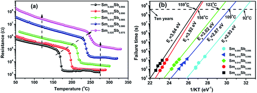
Fig. 1(a) shows the resistance of the Sm doped Sb films (x = 0.005, 0.010, 0.015, 0.020 and 0.025) as a function of temperature at a heating rate of 20 °C min−1. It can be clearly found that the a precipitous drop, defined as the crystallization temperature (Tc), occurs at 165 °C, 191 °C, 209 °C, 231 °C and 243 °C upon increasing the doping content from 0.005 to 0.025. This result reveals that the Sm dopants can significantly inhibit the growth-dominant crystallization process, leading to a remarkable improvement of the thermal stability. In addition, the resistance of the amorphous and crystalline state increases upon increasing the doping content of Sm, indicating a decrease in the writing current of their PCM devices.18The 10 year data retentions of the Sm doped Sb thin films are shown in Fig. 1(b), which can be characterized by extrapolating the isothermal plots in the Arrheniuus equation:
 | (1) |
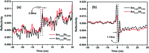
The phase change speed is the key index for materials in data memory, which can be characterized by the change in the optical reflectivity. Fig. 2 shows the evolution of reflectivity for Sm0.005Sb0.995 and Sm0.015Sb0.985 excited by laser irradiation. When excited with a laser pulse of fluence 0.56 mJ cm−2, the reflectivity increases due to the transition from an amorphous to crystalline state, as shown in Fig. 2(a). For comparison, the reverse amorphous-to-crystalline transition was also achieved using a higher laser fluence of 1.72 mJ cm−2, showing a decrease in the optical reflectivity. In Fig. 2(b), the clear peaks with reverse direction may be ascribed to the Sb volatilization or hole opening and propagation upon increasing the laser power.20 Compared with the laser fluence of GST (7.31 mJ cm−2 for the crystallization process and 12.31 mJ cm−2 for the amorphization process),21 the Sm doped Sb materials possess much lower laser fluence, revealing the lower power consumption for phase change. More importantly, Fig. 2 reveals that the crystallization time for the Sm doped Sb films was about 2.08 ns, which is much shorter than GST (∼17 ns)21 and other known Sb-rich alloys such as SbSe (∼11 ns)22 and GeSb (∼12 ns).23 Similarly, the amorphization process has a much shorter time (about 1.74 ns) than GST (∼16 ns) or other systems. Thus, these results demonstrate that the Sm doped Sb thin films have an ultra-high phase change speed due to their growth-dominated crystallization process.24 In general, the Sb-rich materials will have fast phase change speed because of the weak Sb–Sb bond. The doped atoms, such as Sm, will form a new bond such as Sm–Sb, which can easily break the Sb–Sb bond.25 In this study, the ultra-high phase change speed was ascribed to the growth-dominated crystallization mechanism of the Sb–Sb bond. More importantly, the slight Sm doping allows the films to still possess the massive nucleating center of Sb–Sb, keeping the ultra-high phase change speed.
The surface roughness of the films is very important for the device performance because the electric properties depend on the quality of the electrode-film interface.26 Fig. 3 shows the film surface roughness of the Sm doped Sb films observed by AFM. Generally, the root mean square (RMS) is calculated as the root mean square of the surface measured microscopic peaks and valleys, which is the key index for surface roughness. As shown in Fig. 4, the RMS of the as-deposited Sm0.005Sb0.995, Sm0.010Sb0.990, Sm0.015Sb0.985, Sm0.020Sb0.980 are 0.41, 0.34, 0.29 and 0.24 nm, respectively. Compared with other results, such as Sn2Se3 (ref. 27) and Sb2Te3,28 the Sm doped Sb films have a relatively low RMS value, demonstrating the excellent surface roughness for the devices performance. In addition, it is clearly found that the RMS values decrease upon increasing the content of the Sm dopant due to the impediment of the crystallization process by the Sm doping. On this point, the Sm dopants will be propitious to improve the performance of PCM devices.
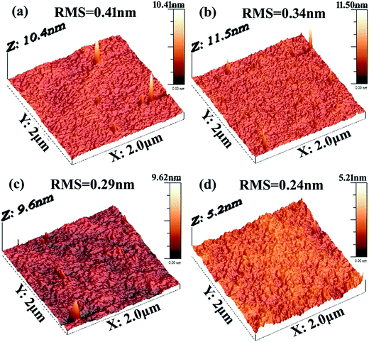 | ||
| Fig. 3 AFM image of the as-deposited (a) Sm0.010Sb0.990, (b) Sm0.015Sb0.985, (c) Sm0.020Sb0.980 and (d) Sm0.025Sb0.975. | ||
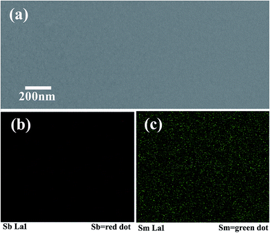 | ||
| Fig. 4 (a) The surface morphology and (b and c) EDS mapping of the as-prepared Sm0.025Sb0.975 thin film. | ||
Fig. 4(a) shows the SEM images of the as-prepared Sm0.025Sb0.975 thin film. It is apparent that no crystalline grains were observed in the film, also indicating the smooth amorphous state. The corresponding EDS elemental mappings are shown in Fig. 4(b) and (c). Through Fig. 4(c), it is apparent that there is a homogeneous distribution of Sm in the Sb thin film. In addition, Fig. 4(b) shows the Sb elemental homogeneous distributed over the surface. These results directly demonstrate that the Sb films are embedded with uniform Sm elements.
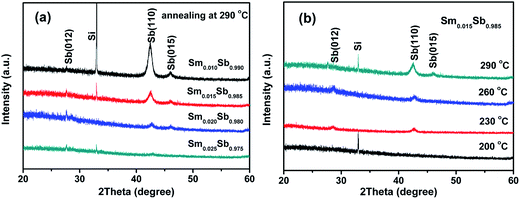
Fig. 5 shows the crystalline structures of the Sm doped Sb films characterized by XRD after annealing in an Ar atmosphere for 5 min. As shown in Fig. 5(a), only the single hexagonal phase of Sb (PDF#35-0732) was observed after annealing at 290 °C. Moreover, Fig. 5(a) also indicates that the intensity of the XRD peaks significantly decreased upon increasing the Sm doping resulting in a significant increase in the Tc, which is in accordance with the R–T measurements. Fig. 5(b) shows the XRD patterns of the Sm0.015Sb0.985 film annealed at different temperatures. It can be seen that when the annealing temperature was lower than 200 °C, the film maintained an amorphous state. When the temperature was higher than 230 °C, the crystallization peaks emerged, which could be assigned to the phase transition. This result reveals that the Sm0.015Sb0.985 thin film can keep a stable amorphous state at 200 °C, indicating excellent thermal reliability for PCM applications.
In order to comprehend the mechanism for the enhanced thermal stability, the bond environments of the doped crystalline films were measured using XPS, as shown in Fig. 6. The XPS analysis in Fig. 6(a) indicates that the Sm–Sb bonds exists in the crystalline Sm doped Sb films, which is consistent with Er doped Sb films.29 Thus, the formation of some Sm–Sb bonds during the crystallization process will increase the Ec and enhance the thermal stability. In addition, Fig. 6(a) also shows that the relative intensity of the Sm–Sb peaks decreases upon increasing the Sm content, which may be attributed to the lower Tc with a lower amount of dopant.30,31 Fig. 6(b) indicates that some Sm–Sm bonds exist in the Sm0.020Sb0.980 film only when the doping content is larger than 0.020. This powerfully illustrates that, with slight Sm doping, the formation of the Sm–Sb bonds plays the main role in the control of thermal stability.
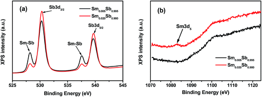 | ||
| Fig. 6 (a) High resolution Sb3d and (b) high resolution Sm3d XPS spectra of the Sm0.005Sb0.995 and Sm0.020Sb0.980 thin films annealed at 290 °C for 5 min. | ||
4. Conclusions
In summary, Sm doped Sb thin films were prepared via RF magnetron sputtering. The crystallization temperature (Tc) and 10 year data retention of the Sm doped Sb films both increase upon increasing the amount of Sm doping and are both higher than those of conventional GST films. A reversible phase transition was achieved by picosecond laser pulses, which indicated that the Sm doped Sb thin films had an ultra-high phase change speed. AFM tests revealed that the SmxSb1−x alloys have excellent surface roughness, and the value of the RMS decreased upon increasing the amount of Sm doping. EDX mapping showed that the Sm elements were homogenously distributed in the Sb thin films. The XRD measurements reveal that the Sm doped Sb films have a single Sb phase and also proved the significant improvement via Sm doping. The XPS analyses show the improvement in the device performance was due to the Sm–Sb bonding. Thus, the outstanding properties of simultaneous high thermal stability and ultra-fast phase change speed make the Sm doped Sb thin films promising candidates for PCM applications.Acknowledgements
This study was supported by the Natural Science Foundation of Jiangsu Province (No. BK20151172) and Changzhou Sci & Tech Program (No. CJ20159049, CJ20160028), and sponsored by the Qing Lan Project.References
- T. H. Lee, D. Loke and S. R. Elliott, Adv. Mater., 2015, 27, 5477–5483 CrossRef CAS PubMed.
- X. Zhou, J. Kalikka, X. Ji, L. Wu, Z. Song and R. E. Simpson, Adv. Mater., 2016, 28, 3007–3016 CrossRef CAS PubMed.
- D. Lencer, M. Salinga, B. Grabowski, T. Hickel, J. Neugebauer and M. Wuttig, Nat. Mater., 2008, 7, 972–977 CrossRef CAS PubMed.
- S. Raoux and D. Ielmini, Chem. Rev., 2009, 110, 240–267 CrossRef PubMed.
- Y. Lu, S. Song, X. Shen, G. Wang, L. Wu, Z. Song, B. Liu and S. Dai, J. Alloys Compd., 2014, 586, 669–673 CrossRef CAS.
- Y. Gu, T. Zhang, Z. Song, Y. Liu, B. Liu and S. Feng, Appl. Phys. A: Mater. Sci. Process., 2010, 99, 205–209 CrossRef CAS.
- P. C. Chang, C. C. Chang, S. C. Chang and T. S. Chin, J. Non-Cryst. Solids, 2014, 383, 106–111 CrossRef CAS.
- H. Zou, X. Zhu, Y. Hu, Y. Sui, W. Wu, J. Xue, L. Zheng and Z. Song, CrystEngComm, 2016, 18, 6365–6369 RSC.
- X. Zhou, L. Wu, Z. Song, F. Rao, K. Ren, C. Peng, S. Song, B. Liu, L. Xu and S. Feng, Appl. Phys. Lett., 2013, 103, 072114 CrossRef.
- K. Ren, F. Rao, Z. Song, C. Peng, J. Li, L. Wu, B. Liu and S. Feng, Appl. Phys. Lett., 2013, 103, 093111 CrossRef.
- S. Y. Lee, H. K. Kim, J. H. Kim, J. S. Roh and D. J. Choi, J. Mater. Sci., 2009, 44, 4354–4359 CrossRef CAS.
- J. Tominaga, T. Nakano and N. Atoda, Appl. Phys. Lett., 1998, 73, 2078–2080 CrossRef CAS.
- H. Zou, X. Zhu, Y. Hu, Y. Sui, Y. Sun, J. Zhang, L. Zheng and Z. Song, J. Appl. Phys., 2016, 120, 245303 CrossRef.
- T. Guo, S. Song, L. Li, X. Ji, C. Li, C. Xu, L. Shen, Y. Xue, B. Liu, Z. Song, M. Qi and S. Feng, Scr. Mater., 2017, 129, 56–60 CrossRef CAS.
- X. Zhu, Y. Hu, H. Zou, J. Zhang, Y. Sun, W. Wu, L. Yuan, L. Zhai, S. Song and Z. Song, Scr. Mater., 2016, 121, 66–69 CrossRef CAS.
- F. Xu, Y. Luo, M. Deng and Q. Shen, Eur. J. Org. Chem., 2003, 2003, 4728–4730 CrossRef.
- C. Gao, H. Song, L. Hu, G. Pan, R. Qin, F. Wang, Q. Dai, L. Fan, L. Liu and H. Liu, J. Lumin., 2008, 128, 559–564 CrossRef CAS.
- X. Zhou, L. Wu, Z. Song, Y. Cheng, F. Rao, K. Ren, S. Song, B. Liu and S. Feng, Acta Mater., 2013, 61, 7324–7333 CrossRef CAS.
- X. Cheng, F. Mao, Z. Song, C. Peng and Y. Gong, Jpn. J. Appl. Phys., 2014, 53, 050304 CrossRef.
- C. Ortiz and A. Blatter, Thin Solid Films, 1992, 218, 209–218 CrossRef CAS.
- Y. Hu, X. Feng, J. Zhai, T. Wen, T. Lai, S. Song and Z. Song, Scr. Mater., 2014, 93, 4–7 CrossRef CAS.
- W. Wu, Y. Hu, X. Zhu, Y. Sui, J. Xue, L. Yuan, S. Song and Z. Song, J. Mater. Sci.: Mater. Electron., 2015, 26, 9700–9706 CrossRef CAS.
- Z. Li, Y. Hu, T. Wen, J. Zhai and T. Lai, J. Appl. Phys., 2015, 117, 135703 CrossRef.
- L. V. Pieterson, M. H. R. Lankhorst, M. V. Schijndel, A. E. T. Kuiper and J. H. J. Roosen, J. Appl. Phys., 2005, 97, 083520 CrossRef.
- W. Wu, S. Chen, J. Zhai, X. Liu, T. Lai, S. Song and Z. Song, Appl. Phys. Lett., 2017, 110, 181906 CrossRef.
- H. Zou, X. Zhu, Y. Hu, Y. Sui, L. Zheng, W. Wu, L. Zhai, J. Xue and Z. Song, J. Mater. Sci.: Mater. Electron., 2017, 28, 3806–3811 CrossRef CAS.
- Y. Hu, S. Li, T. Lai, S. Song, Z. Song and J. Zhai, J. Alloys Compd., 2013, 581, 515–518 CrossRef CAS.
- W. Fenfen, W. Long, K. Tao, S. Lin, H. Rong, Z. Jie and C. Guosheng, Appl. Phys. Lett., 2013, 103, 181908 CrossRef.
- H. Zou, X. Zhu, Y. Hu, Y. Sun, L. Zheng, Y. Sui, S. Wu and Z. Song, J. Mater. Sci., 2017, 52, 5216–5222 CrossRef CAS.
- F. Wei, L. Wang, T. Kong, L. Shi, R. Huang, J. Zhang and G. Cheng, Appl. Phys. Lett., 2013, 103, 181908 CrossRef.
- C. Peng, L. Wu, Z. Song, F. Rao, M. Zhu, X. Li, B. Liu, L. Cheng, S. Feng and P. Yang, Appl. Surf. Sci., 2011, 257, 10667–10670 CrossRef CAS.
| This journal is © The Royal Society of Chemistry 2017 |

