
 Open Access Article
 This Open Access Article is licensed under a
 Creative Commons Attribution 3.0 Unported Licence
A BHJ-thin-film/liquid-electrolyte based electrochemical-sensor for visible light-detection
Ali Sephar Shikoha,
Zubair Ahmad *b,
Farid Touatia,
R. A. Shakoorb,
Jolly Bhadrab and
N. J. Al-Thanib
*b,
Farid Touatia,
R. A. Shakoorb,
Jolly Bhadrab and
N. J. Al-Thanib
aDepartment of Electrical Engineering, College of Engineering, Qatar University, P. O. Box 2713, Doha, Qatar
bCenter for Advanced Materials (CAM), Qatar University, P. O. Box 2713, Doha, Qatar. E-mail: zubairtarar@qu.edu.qa; Tel: +974 4403 7729
First published on 14th July 2017
Abstract
The current study presents a new type of inexpensive and very sensitive bulk heterojunction (BHJ) organic photo-sensor (OPS) configuration that incorporates a layer of liquid electrolyte into the conventional BHJ photodiode arrangement. Initially, a P3HT:PCBM blend based photo-anode was deposited onto ITO substrates using spin coating. Then the semiconductor coated photo-anode was attached to a Pt/ITO counter electrode. A 40 µm gap between photo-anode and counter electrode was filled with a liquid (iodine based) HI-30 electrolyte. Various electrical parameters including ideality factor, series and shunt resistance were extracted from the current–voltage characteristics under dark and light conditions. The value of mobility measured under dark conditions was found to be 25.58 × 10⁻⁶ m2 V−1 s−1. In addition, the samples were found to have a series and shunt resistance of 133.33 Ω and 74.70 kΩ, respectively. Under illumination, the fabricated photodiodes exhibited a linear current–irradiance relationship, with a rapid response time, when exposed to transient light, thus making the newly proposed hybrid BHJ photo-diode configuration a potential alternative to the conventional photo-sensors.
Introduction
Organic photo-sensors (OPSs) have attracted a lot of attention in recent years, owing to their flexibility, low cost, light weight, easy fabrication techniques and broad spectral response.1 In addition, they also create a possibility of processing on a large active area by means of several deposition methods including roll-to-roll and ink-jet printing.2,3 Among others, OPSs are being used in bioelectronics, infrared light detection, data transmission and numerous analytical applications. These detectors can be divided into two major groups i.e. two-terminal photodiodes and three-terminal phototransistors.4 Although the photodiodes are not as sensitive as phototransistors, their linearity in response can, however, make them more attractive in applications involving simple light meters.5Bulk heterojunction (BHJ) is considered as one of the leading organic photodiode configurations, being employed today.6–8 A typical BHJ configuration involves the use of a homogeneous blend of donor (D) polymer and acceptor (A) molecules, that forms an interpenetrating network, with nanoscale heterojunction interface.3,6 This interpenetrating network facilitates the charge collection at respective electrodes by making sure that all photo-generated excitons reach the D/A interface. When operated in reverse biased mode, the same BHJ device structure employed in organic solar cell (OSC) can be operated as organic photodiode (OPD).6 However, in case of BHJ photodetectors, emphasis is paid on parameters like linearity, responsivity, sensitivity etc. rather than power conversion efficiency (required for solar cell performance characterization), since precise and sensitive detection of a signal originating from the sensing film is of key importance for photodiode's performance evaluation.7
For a better operation, it is crucial that the charge transfer process is optimized in order to favor the transfer of photo-induced electrons to the external circuit over recombination with holes. One such approach deals with improving the kinetics of cathode interface. In case of dye-sensitized-photo-sensors (DSPSs), the cathode interface kinetics are immensely dependent on the electrolyte (redox couple based), which provides ionic conductivity between the positive and negative electrodes and is responsible for two main factors: (1) retardation of the recombination process, (2) efficient transportation of charge carriers between the active semiconductor layer and cathode.8,9 When integrated into a BHJ photodiode configuration as an intermediate layer, the electrolyte (redox based) can serve the same functions, thereby improving various photo-detection/sensory parameters including short circuit current (Isc), open circuit voltage (Voc), and sensitivity. Further, with the addition of electrolyte, the charge transport mechanism becomes dependent on the contained ion species, thereby waiving off the constraint of making the active layer of precise thickness and eventually making the fabrication simple, fast and economical. Nevertheless, the use of electrolyte would also eliminate the need of high cost and time consuming counter electrode deposition process that limits the use of BHJ OPDs in many industrial applications.10
In the present work, keeping in view the advantages of the organic BHJ and DSPS structures, a hybrid BHJ/DSPS configuration has been introduced. The current study aims to fabricate inexpensive and high yield hybrid BHJ photodiodes by means of an additional electrolyte layer sandwiched between the semiconductor and cathode. Initially, a semiconductor layer based on PCBM:P3HT blend was spin coated onto ITO substrates. These substrates were later integrated with Pt-based cathodes to fabricate hybrid BHJ-OPDs. Iodolyte HI-30 liquid electrolyte based on I−/I3− redox ion species was utilized for transportation of charge carriers between the semiconductor layer and cathode, owing to its high performance and low viscosity. Finally, the fabricated hybrid PDs (ITO/P3HT:PCBM/electrolyte/Pt) were characterized for various performance criteria under dark and light conditions.
Experimental
Regioregular poly(3-hexylthiophene-2,5-diyl) (P3HT) and phenyl-C61-butyric acid methyl ester (PCBM) chemicals were purchased from Lumtec, Taiwan. 1 wt% solutions of both n-type (PCBM) and p-type (P3HT) materials were prepared separately, in chloroform. To attain homogeneous solution, the vials containing PCBM and P3HT solutions were stirred at 1000 RPM for 24 hours. The preparation of photo-anode started off with the cleaning of ITO slides. The ITO coated glass substrates (purchased from Lumtec) were submerged in acetone and sonicated for a duration of 15 minutes. Later, the slides were washed with acetone and distilled water. At the end of the cleaning process, the slides were dried using a warm air blow dryer. It was made sure that no impurity-induced strains were visible. For the deposition of a PCBM:P3HT BHJ semiconductor layer spin-coating was utilized since it is a simple and relatively easy process; adopted worldwide to deposit thin and uniform coatings on a variety of substrates.11 The homogenized PCBM and P3HT solutions were mixed together in 1![[thin space (1/6-em)]](https://www.rsc.org/images/entities/char_2009.gif) :1 ratio. To deposit the PCBM:P3HT BHJ films, 100 µl of the mixed solution was spread on the whole surface of each ITO substrate (size 2.5 cm × 2.5 cm) and spin-coated at 1000 rpm. The thickness of the deposited BHJ films was noted to be in the range of 110 ± 10 nm. Later, the photo-anodes were annealed at 110 °C for a duration of 30 min (Fig. 1).
:1 ratio. To deposit the PCBM:P3HT BHJ films, 100 µl of the mixed solution was spread on the whole surface of each ITO substrate (size 2.5 cm × 2.5 cm) and spin-coated at 1000 rpm. The thickness of the deposited BHJ films was noted to be in the range of 110 ± 10 nm. Later, the photo-anodes were annealed at 110 °C for a duration of 30 min (Fig. 1).
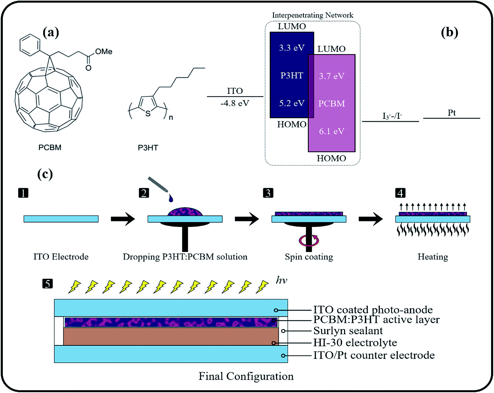 | ||
| Fig. 1 (a) Molecular structure of PCBM and P3HT, (b) energy band diagram, (c) step involved in the preparation of the photo-anode and fabrication of the final configuration of the BHJ photo-diode. | ||
For the photo-sensor fabrication, a sealing mask (Solaronix) was fixed around the edges of the photo-anode BHJ layer and attached to the drilled counter electrode (Solaronix), containing ITO and platinum (Pt) catalyst coatings. The whole assembly was heated at 100 °C, to form a sealed device. It was made sure that cells were properly sealed (without any imperfections) to prevent electrolyte leakage, that would have proved detrimental to the long-term performance of the sensor. For the hole transportation between the semiconductor layer and counter electrode a high performance Iodolyte HI-30 electrolyte was used that is based on I−/I3− ions species (ionic liquid) and comprises of additives including lithium salt, pyridine derivative, thiocyanate dissolved in acetonitrile. The electrolyte was poured into the vacant space between the photoelectrode and counter-electrode, using a vacuum syringe. Finally, the drilled hole (used for pouring electrolyte) was sealed using Meltonix (Solaronix) sealing mask. The fabricated sensors were subjected to performance tests for the characterization of various sensory parameters (including photo-sensitivity and responsivity) under light and dark conditions, using Sunlite solar simulator (manufactured by Abet Technologies) and Keithley 2400 SMU.
Results and discussion
Electrical characteristics
The dark I–V characteristics of the fabricated hybrid photo-detector are depicted in Fig. 2. In the present scenario, the forward bias corresponds to positive potential applied to Pt electrode with respect to ITO. The measured I–V characteristics exhibited a non-linear, asymmetric and rectification behavior. At low voltage levels, the I–V characteristics of the hybrid photodetector showed an exponential increase in the current, whereas at higher voltage (above 0.25 V) the current–voltage relationship was quasi-linear, mainly because of the minimization of the depletion layer, which in turn made the organic film act as a resistor.12 The value of turn-on voltage (Von), estimated from the linear part of the forward biased I–V curve region, was found to be 0.25 V. The rectification ratio (RR) determined using the ratio of forward current to reverse current (IF/IR), turned out be 55.5 at ±0.4 V. The inset in Fig. 2 shows a graph between V and lnI measured in the dark conditions. As observed in the forward biased region, the I–V characteristics were almost linear at low voltage levels. However, at higher voltage levels the characteristics started deviating from linearity and became quickly overpowered by the series resistance presented by the contact wires or bulk resistance of the organic semiconductor material, resulting in a curve at the end of the forward biased region. As soon as the diode became reverse biased, a current was produced due to the diffusion of minority carriers across the potential barrier, which should ideally remain at a constant value until the reverse voltage reached the breakdown limit. This constant current that remained unaffected by the applied potential is called the reverse saturation current (Io).13 In the current case, a Io of 2.74 µA was found graphically as shown in the graph in the inset of Fig. 2.
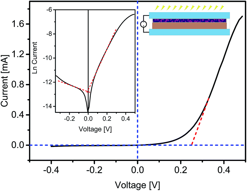 | ||
| Fig. 2 Forward and reverse biased I–V characteristics under dark conditions measured at room temperature, for the fabricated BHJ thin film/electrolyte photo-detector. Inset shows the graph between V vs. lnI in the dark. | ||
The ideality factor (also known as a quality factor) is a figure of merit for a semiconductor diode which provides the information about quality and performance of a semiconductor diode.14 The ideality factor is mainly dependent on the locus of the recombination of the charge carriers (i.e. electron–hole pairs).15 For an ideal diode, with no charge carrier traps and absence of recombination (or occurrence of recombination in the neutral region of p–n junction), the ideality factor should be equal to 1. However, in the case of non-ideal diodes, the ideality factor is greater than unity because of the occurrence of trap facilitated recombination of electrons and free holes, in the space-charge region. If the recombination occurs in the space charge region, mediated by recombination centers in the band gap, the ideality factor increases to 2. Ideality factor can also be greater than 2 and values as high as 20 have been quoted by various studies, in the past.16 Since in dark conditions a BHJ based solar cell/photo-sensor behaves as a diode, therefore the equation describing current (I) as a function of applied voltage (V) for the Schottky junction can be used to calculate the ideality factor, eqn (1). Using eqn (1), the ideality factor was found to be 2.43 ± 0.09. Numerous factors including series resistance, tunneling effects, non-homogeneous thickness of organic film, presence of native oxide layer on electrodes, organic layer effect, voltage drop across interfacial layer and Schottky effect, might be potential reasons of the high ideality factor.12,17
 | (1) |
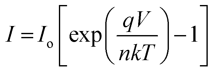
Series (Rs) and shunt resistance (Rsh) play a major role in the performance and reliability of the semiconductor diodes and can be determined by plotting junction resistance (RJ) values as a function of the applied voltage, as shown in Fig. 3. The maximum RJ value (in the reverse biased region) can be considered as a shunt resistance (Rsh). On the other hand, the series resistance (Rs) is the lowest RJ value occurring in the forward region. The Rs and Rsh resistance values were estimated to be 120.19 Ω and 74.71 kΩ, respectively. The abrupt peaks seen in both forward and reverse biased region might be the resultant of any changes occurring in the electrolyte/bulk interface charges under the applied voltages.
 | ||
| Fig. 3 Graph between junction resistance and voltage, presenting the values of Rsh and Rs, inset depicts the logI–logV characteristics of the cell. | ||
Indeed, the transportation of charge carriers in semiconductor diodes involves a series of different conduction mechanism. These mechanism are usually described using a double logI–V graph, in terms of various transport regimes, namely; ohmic, space charge limited current (SCLC) and trap charge limited current (TCLC) regimes. In ohmic region, the current is directly proportional to the applied voltage. In the case of SCLC region, a quadratic relationship exists between current and voltage. This region can be noticed in two situations i.e. with partially filled traps (trapping parameter: Θ < 1) or fully filled traps (Θ = 1).18 TCLC regime exists in-between the ohmic and SCLC region with a Vn dependence of current density on voltage. Higher order dependence of current on voltage can also occur in regimes where mobility is dependent on electric field density. The double logarithmic I–V plot is shown in the inset of Fig. 3. Varied slopes of different regions signify that the conduction mechanism altered with the applied potential difference. The transition between the regions can also be seen clearly. At voltage levels, lower than the turn-on voltage (VT) the slope of the characteristic curve was found to be 1.8. Due to the small magnitude of the applied voltage in this region, the number of injected electrons are lower than the number of thermally generated electrons.19 As a result, the injected electrons are incapable of filling any of the traps located in the organic semiconductor layer. Thus, the injected carriers skipped between the deepest energy traps, making the current almost proportional to the applied potential difference. With further increase of the biased voltage, the slope increased to 3.97, indicating a Vn dependence of current on voltage. Therefore, the region (ranging from 0.17 V to 0.38 V) can be regarded as TCLC region. The higher magnitude of applied potential difference resulted in an increased number of carriers being generated, that can fill the lower energy traps, facilitating the transport of additional carriers in higher energy traps and thus resulting in a higher current (to voltage) increasing ratio. The slope of the third and final region turned out to be ∼2, representing an SCLC region, where all the traps get occupied and the carriers are transported in the organic material without any restriction. The only entity that limited the carriers' transportation is the space charge.
In SCLC region, the charge transport mechanism can be explained by using the Child's law (eqn (2)).
| J = (9εsθµV2)/8d3 | (2) |
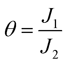 ” is defined as the ratio of current densities at the beginning and at the end of the of square law region, and its value can be calculated from the ratio of current density values J1 and J2, lying at the beginning and end of region III, respectively.20 Using eqn (2) the mobility (µ) was calculated which turned out to be 25.47 × µm2 (V−1 s−1).
Photo-sensor characteristics
Fig. 4(a) shows the current–voltage characteristics of the sensors, as a function of varied irradiance levels. As seen, the magnitude of generated current increased linearly from 0.1 mA to 0.6 mA. When the photo-sensor is illuminated, electron–hole pairs are generated in the P3HT and diffused into the P3HT:PCBM blend interface and split apart due to the built-in electric field. As known, the HOMO level of PCBM is lower as compared to P3HT, thus the holes are transferred from P3HT to PCBM and later to the electrolyte and finally reach to the respective electrode. A similar explanation can be given for the electron transportation. This difference between the HOMO level of PCBM and P3HT is the main reason behind the upsurge in the number of excited electrodes produced, thereby enhancing the photocurrent generation, with respect to increased irradiance levels.21 Typically, the trend of increased photocurrent followed, until a saturation point was reached i.e. maximum number of photoelectrons is being produced, and transferred to the photo-anode. In the case of open circuit voltage (Voc), a similar trend is noted.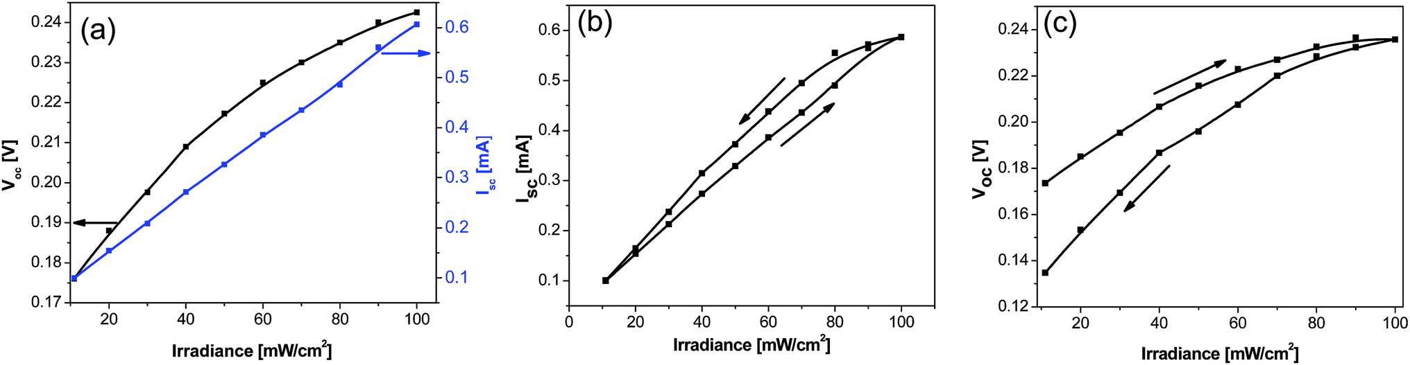 | ||
| Fig. 4 (a) Isc and Voc values measured at different irradiance levels ranging from 11 mW m−2 to 100 mW m−2, (b) Isc values with respect to ascending and descending irradiance levels, (c) Voc values with respect to ascending and descending irradiance levels. | ||
To analyze the hysteresis in Isc and Voc, forward and reverse step irradiance measurements were performed. Initially, the irradiance was increased from 11 mW m−2 to 100 mW m−2 (forward) and the resultant Isc and Voc values were noted. The same procedure was applied in reverse, with the irradiance now decreasing from 100 mW m−2 to 11 mW m−2. When taking measurements in ascending order, the current was seen to rise in a linear fashion, Fig. 4(b). However, the diode started deviating from the ascending irradiance part, owing to the fact that the diode remained saturated till 80 mW m−2. At 80 mW m−2 irradiance level, maximum difference of 65.32 µA was observed. This difference began to diminish as the irradiance was further decreased, until the two lines converged at the 11 mW m−2. A linear trend was also noticed for the forward and reverse Voc vs. illumination cycles, Fig. 4(c). However, the voltage saturation at higher irradiance levels (i.e. 90 mW m−2 and 100 mW m−2) was seen. In contrast to the current measurements, lower Voc levels were observed in the reverse cycle. Further, the difference between the Voc values among the two cycles started increasing for reduced irradiance values and this difference reached the highest value at 11 mW m−2 irradiance.
Fig. 5, shows the photocurrent produced as a function of time under the illumination and dark conditions when 0.15 V potential difference was applied. As seen from the figure, when the sample got excited in the presence of light, a spike is generated indicating the generation of both types of charge carriers. One species of the charge carrier produced recombined at the respective electrode, whereas the other traveled through the active area at a constant velocity, resulting in the plateau region in the transient curve. When the light was ceased, the number of electron–hole pair generated sharply declined, resulting in a tail in the transient current. With the passage of time, the number of charge carriers (generated upon illumination) started to decrease. In the second cycle the current peaked at a relatively lower value, and started stabilizing comparatively quickly. The subsequent transient cycles were almost identical in nature, with an average peak current (measured after stabilization) equal to 0.18 mA. For the stable current cycles, an average transient time constant of 0.43 × 10⁻³ was found by measuring the slope of the transient cycle's tail area. The response time (ts) and reset/recovery time (tc) which are defined as the time required for the photo-current to reach a stable peak value and vice versa, were found to be 0.35 s and 0.23 s, respectively. Further, the responsivity (R) which is the ratio of the photocurrent to illumination power, in the photoconductive mode, was found to have an average value of 1.03 × 10⁻⁷ A W−1. To determine photoconductive sensitivity, eqn (3) was used.22
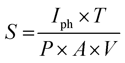 | (3) |
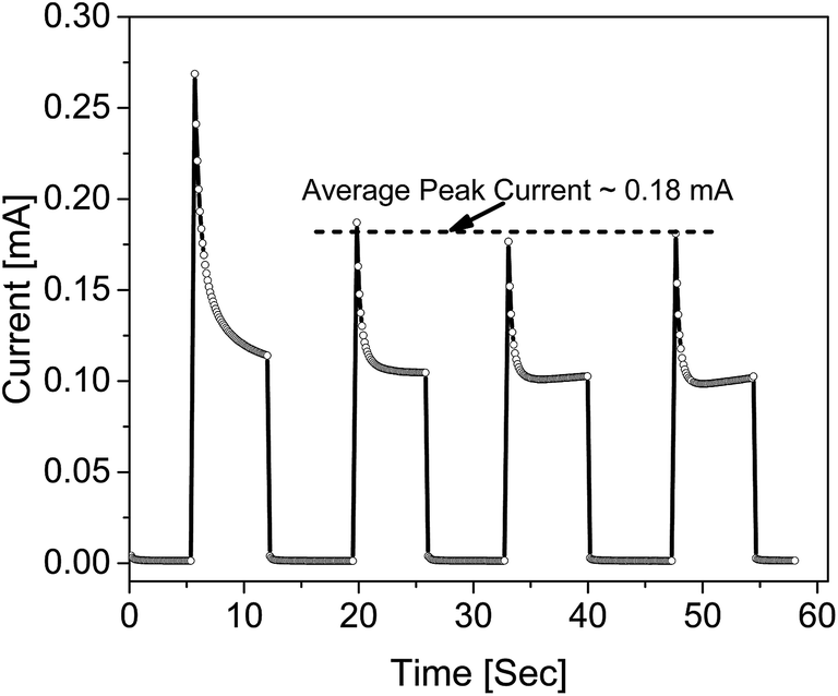 | ||
| Fig. 5 Transient response of the photo-detector. | ||
Conclusion
In the present study, a new type of hybrid BHJ/electrolyte photodetector configuration has been investigated. I–V characteristics exhibited a non-linear, asymmetric and a rectification behavior. The Rs and Rsh resistance values turned out to be 120.19 Ω and 74.71 kΩ, respectively. Under illumination, the photodiodes depicted reasonable photosensitive characteristics with open circuit voltage (Voc) and short circuit current (Isc) vary in a linear fashion with respect to stepped irradiance. Further, the sensors were noted to have a prompt response to any changes in irradiance. The response time and reset/recovery time were found to be 0.35 s and 0.23 s, respectively. These results depict that the new hybrid photo-diode sensor works in an efficient way and can be considered a promising contender in the photo-detection industry.Conflict of interest
The authors declare that there is no conflict of interest.Acknowledgements
This publication was made possible by NPRP grant #5-546-2-2222 from Qatar National Research Fund (a member of Qatar Foundation). The statements made herein are solely the responsibility of the authors. The authors are also grateful to the Center for Advanced Materials (CAM), Qatar University for extended support during this work.References
- M. Burkhardt, W. Liu, C. G. Shuttle, K. Banerjee and M. L. Chabinyc, Appl. Phys. Lett., 2012, 101, 033302 CrossRef
.
- F. Arca, S. F. Tedde, M. Sramek, J. Rauh, P. Lugli and O. Hayden, Sci. Rep., 2013, 3, 1324 CrossRef PubMed
- B. Arredondo, B. Romero, J. M. S. Pena, A. Fernández-Pacheco, E. Alonso, R. Vergaz and C. de Dios, Sensors, 2013, 13, 12266–12276 CrossRef PubMed
- M. C. Hamilton and J. Kanicki, IEEE J. Sel. Top. Quantum Electron., 2004, 10, 840–848 CrossRef CAS
- A. K. Ghosh, Introduction to measurements and instrumentation, PHI Learning Pvt. Ltd., 2012 Search PubMed
- B. Arredondo, C. de Dios, R. Vergaz, G. del Pozo and B. Romero, IEEE Photonics Technol. Lett., 2012, 24, 1868–1871 CrossRef CAS
- E. Manna, T. Xiao, J. Shinar and R. Shinar, Electronics, 2015, 4, 688–722 CrossRef
- A. Mathew, V. Anand, G. M. Rao and N. Munichandraiah, Electrochim. Acta, 2013, 87, 92–96 CrossRef CAS
- J. Wu, Z. Lan, J. Lin, M. Huang, Y. Huang, L. Fan and G. Luo, Chem. Rev., 2015, 115, 2136–2173 CrossRef CAS PubMed
- V. T. H. Pham, T. K. Trinh, N. T. N. Truong and C. Park, Jpn. J. Appl. Phys., 2017, 56, 046501 CrossRef
- W. S. Wong and A. Salleo, Flexible electronics: materials and applications, Springer Science & Business Media, 2009 Search PubMed
- Z. Ahmad, P. Ooi, K. Aw and M. Sayyad, Solid State Commun., 2011, 151, 297–300 CrossRef CAS
- U. Bakshi and A. Godse, Semiconductor Devices & Circuits, Technical Publications, Pune, India, 2008 Search PubMed
- G. Wetzelaer, M. Kuik, M. Lenes and P. Blom, Appl. Phys. Lett., 2011, 99, 153506 CrossRef
- A. Usami, in Nanostructured Materials for Solar Energy Conversion, Elsevier, Amsterdam, 2006, pp. 81–104, DOI:10.1016/B978-044452844-5/50004-4
- K. Tvingstedt and C. Deibel, Adv. Energy Mater., 2016, 6, 1502230 CrossRef
- F. Aziz, K. Sulaiman, W. K. Al-Rawi, Z. Ahmad, M. Sayyad, K. S. Karimov, L. Wei and M. Tahir, Pigm. Resin Technol., 2015, 44, 148–156 CrossRef CAS
- A. Vercik, MRS Online Proc. Libr., 2014, 1660 DOI:10.1557/opl.2014.702
- S. Mondal, J.-L. Her, K. Koyama and T.-M. Pan, Nanoscale Res. Lett., 2014, 9, 3 CrossRef PubMed
- Z. Ahmad, M. H. Sayyad and K. S. Karimov, J. Semicond., 2010, 31, 074002 CrossRef
- A. S. Shikoh, Z. Ahmad, F. Touati, R. Shakoor, N. Al-Thani, Z. Zhu, T. Mankowski, M. A. Benammar, M. Mansuripur and C. M. Falco, RSC Adv., 2016, 6, 53123–53129 RSC
- K. W. Qadir, Z. Ahmad and K. Sulaiman, J. Nanopart. Res., 2014, 16, 2705 CrossRef
- B. Hailegnaw, G. Adam and T. Yohannes, Thin Solid Films, 2015, 589, 272–277 CrossRef CAS
- S. Li, D. Xue, W. Xu, Y. Feng, J. Wang, G. Zhang, X. Meng, C. Wang, Y. Song and C. Shu, J. Mater. Chem. C, 2014, 2, 1500–1504 RSC
| This journal is © The Royal Society of Chemistry 2017 |