 Open Access Article
CdS–MoS2 heterostructures on Mo substrates via in situ sulfurization for efficient photoelectrochemical hydrogen generation†
Xianglin Zhua,
Peng Wang*a,
Qianqian Zhanga,
Zeyan Wanga,
Yuanyuan Liua,
Xiaoyan Qina,
Xiaoyang Zhanga,
Ying Dai b and
Baibiao Huang
 *a
*a
aState Key Laboratory of Crystal Materials, Shandong University, Jinan 250100, China. E-mail: pengwangicm@sdu.edu.cn; bbhuang@sdu.edu.cn; Fax: +86-0531-88365969; Tel: +86-0531-88366139
bSchool of Physics, Shandong University, Jinan 250100, China
First published on 15th September 2017
Abstract
A CdS–MoS2 photoelectrode with a double-layer core–shell structure was prepared using a simple electrodeposition–in situ sulfurization method on a Mo substrate. The photocatalytic activity of as-prepared electrodes was evaluated using a photoelectrochemical H2-generation experiment. The photocurrent and photon–electron conversion efficiency of the CdS–MoS2 photoelectrode were nearly double those of a CdS photoanode prepared on FTO glass. The high activity of the CdS–MoS2 photoelectrode was due to the higher separation efficiency of carriers caused by the formed CdS–MoS2 Janus heterojunction structure, which made directional transmission and electron–hole separation possible. Our experiments show that, in addition to being a good co-catalyst in powder material for photocatalytic hydrogen production, MoS2 can also be used as an electron acceptor layer to enhance electron–hole separation.
1. Introduction
The development of modern society has been built on energy consumption, with large amounts of fossil fuels, including coal, oil, and natural gas, burned to power the fast development of the world economy over the last hundred years. However, these fossil fuels are nonrenewable and cause environmental damage. Environmental problems caused by burning fossil fuels have attracted global attention. An ideal energy source to replace fossil fuels would be an effective solution for energy and environmental problems. Solar energy is abundant and clean, making it an excellent candidate. Solar energy conversion has become a hot topic in recent years.1–12 Storing solar energy in the form of hydrogen energy using photoelectrochemical (PEC) water splitting technology is considered a promising solution to provide ample clean energy to satisfy the increasing demands of modern society.13,14In harnessing solar energy to split water with the necessary efficiency, the most important factors are light capture and carrier separation. Some n-type semiconductor photoanodes have shown the ability to split water at low over-potentials, such as TiO2, ZnO, and WO3, and their applications in PEC water splitting have received much attention. Due to self-defects, these materials can only absorb pure UV light or have poor stabilities under sunlight irradiation,15–21 greatly limiting the use of solar energy. Accordingly, developing photoanodes with narrow band gaps that can absorb and utilize visible light is essential to enhance photoelectric water splitting efficiency. CdS, a well-known semiconductor material for PEC water splitting, has outstanding potential due to its excellent visible light absorption properties. The activity of CdS photoanodes is mainly limited by the efficiency of photogenerated carrier separation. Several types of CdS-based photoelectrodes have been developed with high efficiency in PEC hydrogen production, including CdS/TiO2, CdS/ZnO, and CdS/ZnS.22–24 However, preparation of these structures is usually complicated, with the facile construction of CdS photoanodes with high activity remaining a challenge. Among various exploratory approaches to the promotion of carrier transport and separation, constructing a core–shell structure has been shown to be especially advantageous for promoting carrier separation and improving stability owing to the separation of reduction and oxidation sites.25–32
Herein, we have synthesized CdS photoanodes on a Mo mesh substrate using an electrodeposition sulfurization method, which produces a layer of MoS2 between CdS and Mo metal during sulfurization. Experiments showed that the generated CdS and MoS2 layers formed a double-layer shell around an Mo core. Furthermore, the CdS and MoS2 layers formed a special CdS/MoS2 Janus heterojunction that was able to promote the directional transmission of photogenerated electrons and enhance photocatalytic performance.
2. Experimental sections
2.1. Materials and reagents
All reagents used in experiments, including CdCl2, Na2SO4, Na2SO3, and Na2S, were purchased from Aladdin reagent and used without further purification. Mo mesh (99.9%) was soaked in 20% hydrochloric acid for 24 h, and then cleaned ultrasonically with deionized water, ethanol, and acetone for 20 min before use.2.2. Preparation of CdS–MoS2 photoelectrodes
CdS–MoS2 photoelectrodes were prepared using an electrodeposition-sulfurization method. Firstly, Cd metal was electroplated onto Mo mesh in 20 mM CdCl2 solution at a bias voltage of −1.0 V using a three-electrode system comprising a platinum plate counter electrode and saturated Ag/AgCl reference electrode. Different amounts of Cd were deposited by adjusting the deposition time and deposition charge, (0.5 C, 1.0 C, 2.0 C, 3.0 C, and 5.0 C). The prepared electrodes were denoted CdS–MoS2-x, where x is the deposition charge. The deposition current was about 3 mA and two-thirds of the Mo mesh was kept submerged in the solution throughout the process. The deposited electrode was dried with pure N2. The Mo mesh was then sulfurized under an H2S atmosphere by heating to 500 °C at a rate of 10 °C min−1 and then holding at 500 °C for 1 h. Pure N2 was used to purge remaining H2S during cooling. During sulfurization, some Mo also reacted with H2S gas, producing a layer of MoS2 between the Mo core and CdS shell.For comparison, CdS photoelectrodes without the MoS2 layer were prepared on a fluorine-doped tin oxide (FTO) glass substrate, as the Cd layer was too thin to prevent MoS2 generation when using Mo metal as substrate. Typically, CdS/FTO photoelectrodes were prepared according to a literature method,36 but with the reaction time increased to 10 h to achieve the best photoelectric properties.
2.3. Characterization
The structure of the CdS–MoS2 photoelectrode was characterized by X-ray diffraction (XRD) on a Bruker AXS D8 advance powder diffractometer (Cu Kα X-ray radiation, λ = 0.154![[thin space (1/6-em)]](https://www.rsc.org/images/entities/char_2009.gif) 056 nm). The morphology of the as-prepared photoelectrodes was obtained using scanning electron microscopy (SEM, Hitachi S4800). The light source was a 300 W Xe arc lamp (PLS-SXE 300, Beijing Trusttech Co. Ltd.) equipped with an AM 1.5 filter. The amount of H2 produced was determined by gas chromatography (GC, Varian GC-3800) equipped with a thermal conductivity detector.
056 nm). The morphology of the as-prepared photoelectrodes was obtained using scanning electron microscopy (SEM, Hitachi S4800). The light source was a 300 W Xe arc lamp (PLS-SXE 300, Beijing Trusttech Co. Ltd.) equipped with an AM 1.5 filter. The amount of H2 produced was determined by gas chromatography (GC, Varian GC-3800) equipped with a thermal conductivity detector.
2.4. Electrochemical measurements
The photoelectrochemical activity of CdS photoelectrodes was evaluated in a quartz cell using a three-electrode system based on a Chenghua electrochemical work station (CHI660C, Shanghai). A Pt plate and commercially available Ag/AgCl electrode were used as the counter electrode and reference electrode, respectively, with the prepared CdS photoelectrode used as the working electrode. The electrolyte used in all measurements was an aqueous solution containing 0.1 M Na2SO4, 0.05 M Na2S, and 0.05 M Na2SO3 at pH 12.6.3. Results and discussion
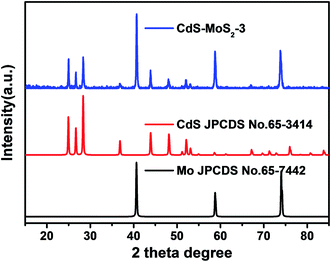
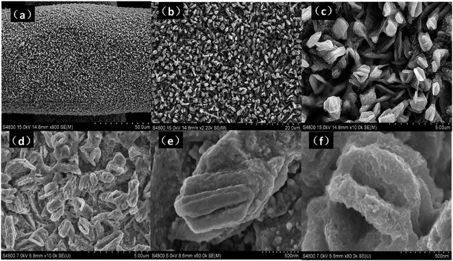
The phase and composition of the CdS–MoS2 photoelectrode were investigated, with Fig. 1 showing the X-ray diffraction (XRD) patterns of CdS–MoS2. The blue line is the pattern for CdS–MoS2, while red and black lines correspond to the standard cards of hexagonal phase CdS and Mo metal, respectively. The XRD results show that the prepared CdS was pure hexagonal phase with good crystallinity. Typically, photocatalytic activity is closely correlated with photocatalyst crystallinity, with good crystallinity usually benefitting the photocatalytic reaction. No obvious MoS2 peaks could be distinguished, meaning that very little MoS2 was formed during the reaction.The surface morphology of the CdS–MoS2 photoelectrode was characterized by SEM. Fig. 2(a–d) show images of the CdS–MoS2 photoelectrode before the photocatalytic experiment. As shown in Fig. 2(a) and (b), CdS was generated on the surface of MoS2 and the Mo mesh with uniform morphology. The magnified SEM images (Fig. 2(c) and (d)) showed plate-like CdS with heights of about 1.2 μm (Fig. S1b†) embedded uniformly in the surface. This plate-like CdS can increase the reaction area, which improves photoelectric activity. Fig. 2(e) and (f) show surface images of CdS after the photocatalytic experiment. The surface of plate-like CdS became rough, perhaps due to photocorrosion.
To further investigate the internal composition and structure of CdS–MoS2 samples, the electrodes were immersed in 1 M HCl solution for 30 min (CdS can react with dilute hydrochloric acid, CdS + HCl → H2S↑ + CdCl2, while MoS2 is more stable in dilute hydrochloric acid solution) to remove surface CdS. The surface elemental composition before and after treatment with HCl solution was analyzed by EDS mapping (Fig. 3(a–e)). The results before HCl treatment confirmed the uniform distribution of Cd and S, with no Mo element detected. This indicated that the CdS layer was compact and could fully cover the electrode surface. The mapping results after treatment with HCl solution showed that only a small amount of elemental Cd existed and that its distribution was uneven, while Mo and S remained uniformly distributed. From the above EDS mapping characterizations, it was concluded that a Mo–S compound was generated under the CdS layer.
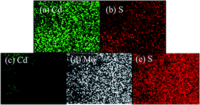 | ||
| Fig. 3 EDS element mapping results of the CdS–MoS2 electrode (a, b) before and (c–e) after treating with HCl solution. | ||
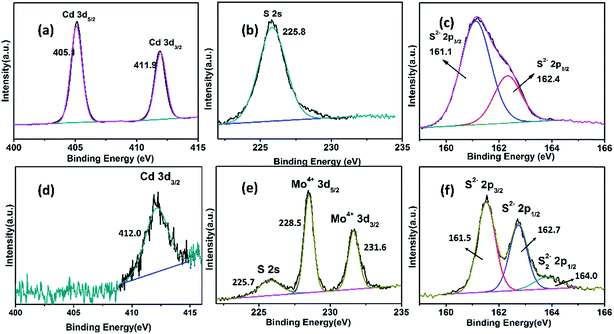
The electrodes before and after HCl solution treatment were analyzed by X-ray photoelectron spectroscopy (XPS). Cd 3d, Mo 3d, and S 2p spectra are shown in Fig. 4. The spectra of untreated samples showed characteristic Cd 3d, S 2s, and S 2p peaks, but no elemental Mo peaks were found. After treatment with HCl solution, the XPS results were very different. The intensity of the Cd 3d peaks became weaker, with only one Cd 3d3/2 peak distinguishable at 412.1 eV. Another characteristic peak at around 405.3 eV was not clearly observed. The XPS of Cd also showed that most elemental Cd was removed by HCl solution. The Mo 3d XPS spectra were resolved into four peaks at around 231.6 eV and 228.5 eV that were assigned to Mo4+ 3d3/2 and Mo4+ 3d5/2, respectively.34 The S 2p XPS spectra were resolved into three peaks, corresponding to two components. Peaks at 162.7 eV and 161.5 eV were attributed to S 2p3/2 and S 2p1/2 signals in MoS2, while the peak at around 164.0 eV was attributed to bridging disulfides, S22−, which have been reported previously35 XPS of Mo and S indicated that MoS2 was formed beneath the CdS layer. Notably, Mo0 was not detected by XPS, proving that the Mo0 core was completed covered with a MoS2 layer.
From the XPS and EDS results, we concluded that the prepared CdS–MoS2 electrodes contained a CdS–MoS2–Mo double-layer core–shell structure. To understand the interactions of CdS and MoS2, Mott–Schottky plots of CdS/MoS2 and CdS/FTO photoanodes were produced, as shown in Fig. S4.† These plots showed that the flat band potential of CdS shifted toward high voltage for the existing of MoS2 layer, indicating heterojunction formation.37,38 In such a structure, the CdS and MoS2 layers construct a CdS/MoS2 type-I heterojunction with a Janus structure. Therefore, photogenerated electrons in the CdS layer are likely transferred to the MoS2 layer under visible light irradiation, while holes remain in the CdS layer, resulting in the separation of photogenerated electrons and holes. This type of CdS/MoS2 Janus structure is advantageous for the directional transmission of carriers and enhances photoelectric activity.33 In the CdS/FTO photoanodes, CdS contacted with FTO directly and there was no forced directional transmission of the photogenerated carriers. Therefore, the CdS/FTO photoanodes showed weaker activity than the prepared CdS–MoS2 photoelectrodes.
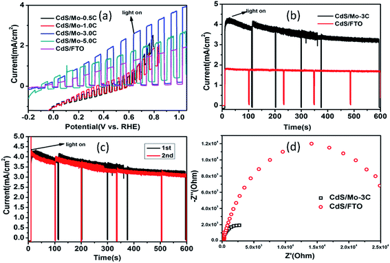
To further examine the activity of CdS–MoS2 photoelectrodes in PEC cells, electrochemical experiments were performed using a three-electrode system. Fig. 5(a) shows current–potential curves of the as-prepared CdS–MoS2 photoelectrodes and CdS/FTO photoelectrodes. Linear sweep voltammograms of the electrodes were recorded under light illumination and in the dark intermittently at a rate of 5 mV s−1. The results show that activity was affected by deposition amount. When the deposition electric charge was 0.5 C or 1.0 C, the prepared CdS–MoS2 photoelectrodes showed poor activity. Furthermore, the dark current was very high during experiments, proving that electric leakage was occurring. CdS–MoS2-3 and CdS–MoS2-5 showed good photoelectric activities, while CdS–MoS2-3 showed the better performance. The deposition amount also influenced the initial potential, with higher deposition amounts corresponding to lower initial potentials. For comparison, the linear sweep voltammogram results of the CdS/FTO electrode were also characterized, as shown in Fig. 5(a). The results show that the prepared CdS/FTO photoelectrode had good photoelectric activity, but worse than that of CdS–MoS2-3 and CdS–MoS2-5. Considering the photoelectric activity and initial potential, a deposition amount of 3C was deemed the most appropriate.
Fig. 5(b) and (c) show I–t curves of photoelectrodes at a potential of 0.9 V vs. RHE. The stable light current density of CdS–MoS2-3 was about 3.5 mA cm−2, while that of CdS/FTO was about 1.7 mA cm−2. During the experiment, CdS/FTO showed good stability, while the light current density of CdS–MoS2-3 decreased to 3.5 mA cm−2 from 4.0 mA cm−2 in 600 s. The cycling experiment of CdS–MoS2-3 after electrolyte replication, as shown in Fig. 5(c), showed no obvious change in activity in the second test, demonstrating that the CdS–MoS2-3 photoelectrode had good stability in the photoelectric test. EDS analysis (Fig. S2†) showed that the ratio of S and Cd elements after photocatalytic reaction was larger than that before the test. This indicated that the decrease of photoactivity was due to sulfur deposition during the reaction caused by oxidation of S2−.
Efficient charge transfer was further verified by electrochemical impedance spectra (EIS).33 Fig. 5(d) shows EIS results for CdS–MoS2-3 and CdS/FTO photoelectrodes under UV-visible light irradiation. The results show that the EIS curve diameter for CdS–MoS2-3 was smaller than that of CdS/FTO, with a smaller radius diameter corresponding to smaller charge-transfer resistance in the EIS Nyquist plot, better electroconductivity, and faster separation efficiency of photogenerated electron–hole pairs on the Cd/Mo electrodes compared with the CdS/FTO sample.
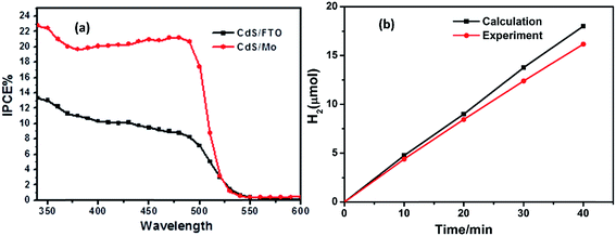
Incident photon-to-electron conversion efficiency (IPCE) is an important index for evaluating photoelectrode activity, and was characterized, as shown in Fig. 6(a). The black and red lines correspond to the IPCE results of the CdS/FTO electrode and the CdS–MoS2-3 electrode, respectively. The IPCE of the CdS–MoS2-3 electrode was higher than that of the CdS/FTO electrode. Furthermore, the IPCE of the CdS–MoS2-3 electrode in the wavelength range 420–500 nm was more than twice that of the CdS/FTO electrode. The IPCE results showed that CdS–MoS2 on the Mo substrate could convert more solar energy than that on FTO glass. The faradaic efficiency was calculated using a photoelectric water splitting experiment. The graph in Fig. 6(b) shows that H2 generation was good and linear, and that the faradaic efficiency of the CdS–MoS2-3 photoelectrode was over 90%.
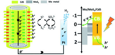
Based on the above experiments and characterization results, we have proposed a possible mechanism to explain the better performance of CdS–MoS2 photoelectrodes compared with the CdS/FTO electrode, as shown in Fig. 7. During Cd sulfurization, some Mo metal reacts with H2S, forming a MoS2 layer between CdS and the Mo substrate. On the CdS anode, photogenerated holes are captured by S2−, while electrons are more likely to migrate to the counter electrode and generate H2. The formed CdS/MoS2 Janus heterojunction takes advantage of the separation of photogenerated electrons and holes along the given direction, which can enhance the carrier separation efficiency. As a result, the prepared CdS–MoS2 structure showed high photoelectric activity.
4. Conclusion
In summary, efficient CdS–MoS2 photoelectrodes were prepared using a simple electrodeposition-sulfurization method. The CdS–MoS2 photoelectrodes had higher activities in photoelectric water splitting than CdS/FTO electrodes. EDS and XPS characterization indicated that the prepared electrodes had a unique CdS–MoS2–Mo double-layer core–shell structure. The presence of a Janus CdS/MoS2 heterojunction was favorable for directional transmission and electron–hole separation. Therefore, the CdS–MoS2 photoelectrodes showed improved activity. These results confirm that, in addition to being a good co-catalyst in powder materials for photocatalytic hydrogen production, MoS2 can enhance the separation efficiency of photoelectrodes by forming a heterojunction. The preparation of these CdS–MoS2 photoanodes will aid the further design of highly efficient photoanodes.Conflicts of interest
There are no conflicts to declare.Acknowledgements
This work is financially supported by the National Basic Research Program of China (the 973 program, 2013CB632401), the National Natural Science Foundation of China (21333006, 21573135, 11374190, 51602179, and 51321091). P. Wang acknowledges support from The Recruitment Program of Global Experts, China. B. B. H. acknowledges support from the Taishan Scholars Program of Shandong Province.References
- K. Sekizawa, K. Maeda, K. Domen, K. Koike and O. Ishitani, J. Am. Chem. Soc., 2013, 135, 4596–4599 CrossRef CAS PubMed.
- J. G. Yu, J. X. Low, W. Xiao, P. Zhou and M. Jaroniec, J. Am. Chem. Soc., 2014, 136, 8839–8842 CrossRef CAS PubMed.
- X. Zong, H. J. Yan, G. P. Wu, G. J. Ma, F. Y. Wen, L. Wang and C. Li, J. Am. Chem. Soc., 2008, 130, 7176–7177 CrossRef CAS PubMed.
- Q. Li, B. D. Guo, J. G. Yu, J. R. Ran, B. H. Zhang, H. J. Yan and J. R. Gong, J. Am. Chem. Soc., 2011, 133, 10878–10884 CrossRef CAS PubMed.
- Q. L. Tay, X. H. Wang, X. Zhao, J. D. Hong, Q. Zhang, R. Xu and Z. Chen, J. Catal., 2016, 342, 55–62 CrossRef CAS.
- T. Kamegawa, H. Seto, S. Matsuura and H. Yamashita, ACS Appl. Mater. Interfaces, 2012, 4, 6635–6639 CAS.
- X. L. Zhu, P. Wang, B. B. Huang, X. C. Ma, X. Y. Qin, X. Y. Zhang and Y. Dai, Appl. Catal., B, 2016, 199, 315–322 CrossRef CAS.
- W. Z. Zhong, T. Qiao, J. Dai, L. Q. Mao, Q. Xu, G. Q. Zou, X. X. Liu, D. L. Yin and F. P. Zhao, J. Catal., 2015, 330, 208–221 CrossRef CAS.
- M. Navlani-García, K. Mori, A. Nozaki, Y. Kuwahara and H. Yamashita, Ind. Eng. Chem. Res., 2016, 55, 7612–7620 CrossRef.
- S. S. Chen, Y. Qi, Q. Ding, Z. Li, J. Y. Cui, F. X. Zhang and C. Li, J. Catal., 2016, 339, 77–83 CrossRef CAS.
- Z. K. Zheng, T. Tachikawa and T. Majima, J. Am. Chem. Soc., 2014, 136, 6870–6873 CrossRef CAS PubMed.
- Q. J. Xiang, J. G. Yu and M. Jaroniec, J. Am. Chem. Soc., 2012, 134, 6575–6578 CrossRef CAS PubMed.
- A. Fujishima and K. Honda, Nature, 1972, 238, 37–38 CrossRef CAS PubMed.
- W. Q. Fan, C. Chen, H. Y. Bai, B. F. Luo, H. Q. Shen and W. D. Shi, Appl. Catal., B, 2016, 195, 9–15 CrossRef CAS.
- J. H. Han, Z. F. Liu, K. Y. Guo, X. Q. Zhang, T. T. Hong and B. Wang, Appl. Catal., B, 2015, 179, 61–68 CrossRef CAS.
- L. P. Wu, Y. L. Zhang, L. Z. Long, C. P. Cen and X. J. Li, RSC Adv., 2014, 4, 20716 RSC.
- M. Kodera, H. Urabe, M. Katayama, T. Hisatomi, T. Minegishi and K. Domen, J. Mater. Chem. A, 2016, 4, 7658–7664 CAS.
- C. Fàbrega, S. Murcia-López, D. Monllor-Satoca, J. D. Prades, M. D. Hernández-Alonso, G. Penelas, J. R. Morante and T. Andreu, Appl. Catal., B, 2016, 189, 133–140 CrossRef.
- R. Lv, T. Wang, F. L. Su, P. Zhang, C. J. Li and J. L. Gong, Nano Energy, 2014, 7, 143–150 CrossRef CAS.
- G. M. Wang, H. Y. Wang, Y. C. Ling, Y. C. Tang, X. Y. Yang, R. C. Fitzmorris, C. C. Wang, J. Z. Zhang and Y. Li, Nano Lett., 2011, 11, 3026–3033 CrossRef CAS PubMed.
- S. C. Wang, H. J. Chen, G. P. Gao, T. Butburee, M. Q. Lyu, S. Thaweesak, J.-H. Yun, A. Du, G. Liu and L. Z. Wang, Nano Energy, 2016, 24, 94–102 CrossRef CAS.
- J. Zhang, L. H. Wang, X. H. Liu, X. A. Li and W. Huang, J. Mater. Chem. A, 2015, 3, 535–541 CAS.
- B. K. Liu, Y. F. Xue, J. T. Zhang, D. J. Wang, T. F. Xie, X. Y. Suo, L. L. Mu and H. Z. Shi, Electrochim. Acta, 2016, 19, 370–376 CrossRef.
- H. Li, C. Z. Yao, L. X. Meng, H. Sun, J. Huang and Q. J. Gong, Electrochim. Acta, 2013, 108, 45–50 CrossRef CAS.
- Y. F. Tang, X. L. Liu, C. C. Ma, M. J. Zhou, P. W. Huo, L. B. Yu, J. M. Pan, W. D. Shi and Y. S. Yan, New J. Chem., 2015, 39, 5150–5160 RSC.
- E. Ha, L. Y. S. Lee, H.-W. Man, S. C. E. Tsang and K.-Y. Wong, ACS Appl. Mater. Interfaces, 2015, 7, 9072–9077 CAS.
- W. W. Xu, Z. Q. Xie, Z. Wang, G. Dietrich and Y. Wang, J. Mater. Chem. A, 2016, 4, 19011–19018 CAS.
- Y. N. Tang, W. H. Di, X. S. Zhai, R. Y. Yang and W. P. Qin, ACS Catal., 2013, 3, 405–412 CrossRef CAS.
- J. K. Zhang, Z. B. Yu, Z. Gao, H. B. Ge, S. C. Zhao, C. Q. Chen, S. A. Chen, X. L. Tong, M. H. Wang, Z. F. Zheng and Y. Qin, Angew. Chem., Int. Ed., 2016, 55, 1–6 CrossRef.
- J. Y. Zhang, Y. H. Wang, J. Jin, J. Zhang, Z. Lin, F. Huang and J. G. Yu, ACS Appl. Mater. Interfaces, 2013, 5, 10317–10324 CAS.
- Y. Zhu, Y. J. Wang, Q. Ling and Y. F. Zhu, Appl. Catal., B, 2017, 200, 222–229 CrossRef CAS.
- F. Liu, W. Q. Yao, D. Liu, R. L. Zong, M. Zhang, X. G. Ma and Y. F. Zhu, Appl. Catal., B, 2015, 163, 547–553 CrossRef.
- P. Wu, C. G. Tian, Y. Q. Jiao, Q. Yan, G. Y. Yang and H. G. Fu, Appl. Catal., B, 2017, 203, 955–963 CrossRef.
- Y. Liu, Y.-X. Yu and W.-D. Zhang, J. Phys. Chem. C, 2013, 117, 12949–12957 CAS.
- H. Vrubel, D. Merki and X. Hu, Energy Environ. Sci., 2012, 5, 6136–6144 CAS.
- G. Bao, C. F. Wang, L. Dong, C. Y. Shen, K. Zhao and C. F. Pan, Nanoscale, 2016, 8, 8078–8082 RSC.
- Z. L. Wang, H. Y. Zhang, H. W. Cao, L. C. Wang, Z. Y. Wan, Y. F. Hao and X. T. Wang, Int. J. Hydrogen Energy, 2017, 42, 17394–17402 CrossRef CAS.
- M. Y. Zhang, H. L. Lin, J. Cao, X. M. Guo and S. F. Chen, Chem. Eng. J., 2017, 321, 484–494 CrossRef CAS.
Footnote |
| † Electronic supplementary information (ESI) available. See DOI: 10.1039/c7ra06304k |
| This journal is © The Royal Society of Chemistry 2017 |

