 Open Access Article
Near-infrared emitting CdTeSe alloyed quantum dots: Raman scattering, photoluminescence and single-emitter optical properties†
Le Xuan Hungab,
Pascal D. Bassènecd,
Pham Nam Thangbe,
Nguyễn Thu Loance,
Willy Daney de Marcillacc,
Amit Raj Dhawanfc,
Fu Fengc,
Juan U. Esparza-Villac,
Nguyen Thi Thuc Hiena,
Nguyen Quang Lieme,
Laurent Coolenc and
Pham Thu Nga*abe
aInstitute of Research and Development, Duy Tan University, Danang, Vietnam. E-mail: ngalamvn@gmail.com
bGraduate University of Science and Technology, Vietnam Academy of Science and Technology, 18 Hoang Quoc Viet Road, Cau giay Dist., Hanoi, Vietnam
cSorbonne Universités, UPMC Univ Paris 06, UMR 7588, Institut de NanoSciences de Paris (INSP), Paris F-75005, France
dGroupe de Laboratoires Physique des Solides et Sciences de Matériaux (GPLSSM), Université Cheikh Anta Diop de Dakar (UCAD), Senegal
eInstitute of Materials Science, Vietnam Academy of Science and Technology, 18 Hoang Quoc Viet Road, Cau Giay Dist., Hanoi, Vietnam
fInstitute of Fundamental and Frontier Sciences, University of Electronic Science and Technology of China, Chengdu 610054, People's Republic of China
First published on 12th October 2017
Abstract
The synthesis of ternary core/shell zinc-blende CdTeSe/ZnSe quantum dots with optimal synthesis parameters is analyzed. For the synthesis of the ternary-alloy CdTeSe core, a temperature around 260 °C is shown to allow a good reaction of both the Te and Se reagents, while for lower temperatures mostly-CdTe quantum dots are synthesized. At this temperature, by changing the ratio of the Te and Se reagents, the composition can be tuned from Te-rich to Se-rich while keeping a constant quantum dot size. The photoluminescence wavelength expands up to 860 nm for the core CdTeSe and 900 nm for the CdTeSe/ZnSe samples, a near-infrared bandgap with potential applications in photovoltaics. The use of Raman spectroscopy is proved especially useful to analyze the composition of the alloy quantum dots, with the presence of two longitudinal-optical phonon lines corresponding respectively to CdTe and CdSe vibrations. For single core/shell CdTeSe/ZnSe quantum dots, perfect single-photon emission is demonstrated with good stability and low blinking, and a long decay time of 110 ns suggesting high luminescence quantum yield.
Introduction
Colloidal quantum dots (QDs) are the subject of intense research programs and innovations to be used in different fields such as solar cells, photocatalysis, light-emitting diodes or biosensors.1–6 Numerous studies on types of QDs that can absorb strongly in the near-infrared (NIR) range (700–900 nm) are currently being conducted, since these QDs can be used as an absorber of solar radiation.7–11 Alloy QDs have attracted great attention due to the enhanced chemical stability resulting from a hardened lattice structure, higher crystallinity, decreased inter diffusion processes and higher photoluminescence quantum yields.12 The optoelectronic properties of alloyed QDs can be tuned by their composition without changing the particle size.13 Besides, ternary alloy cadmium selenide telluride (CdTexSe1−x) QDs can absorb at lower energies when compared with their parent binary CdSe and CdTe QDs, so that, alloyed ternary QDs have many significant advantages compared to their parent binary semiconductors. The possibility to tune both their size and composition, possibly including composition gradients in the material, offers additional degrees of freedom. In particular, due to the optical bowing effect, the absorption and emission wavelengths of the ternary alloy can be redshifted further than for its parent binary semiconductors. For instance, for CdTeSe QDs, expansion of the absorption range up to ∼900 nm has been reported.3,4 CdTexSe1−x alloyed QDs with water-soluble mercaptopropionic acid (MPA) ligand were investigated in 2013 by Pan et al.11,13 applied in a liquid junction QD sensitized solar cell. In11 CdTexSe1−x alloyed QDs were used for the first time in solid state organic solar cells.Many fabrication methods have been studied and improved to synthesize CdTeSe QDs with core/shell structure,14–19 and different kinds of shells such as ZnSe or ZnTe have been reported lately.20 Due to the reactivity difference between Te and Se, a CdTe-rich core and CdSe-rich shell have been formed in the CdTeSe alloy with the formation of a gradient type II.21 This study was carried out with the aim to understand more thoroughly the conditions to fabricate CdTeSe QDs that only crystallize in the zinc-blende single crystalline phase, by using a simple modified fabrication method described in.13,17,22–25 CdTeSe/CdS had been used in quantum-dot-sensitized solar cells with power conversion efficiency achieving over 9%.7 Recently, Poplawsky et al. showed the role of the CdTeSe layer as a NIR photoactive layer in CdTe-based solar cells26 and for using them in quantum-dot-sensitized solar cells (QDSC), we have conducted detailed studies on this material.
In this paper, we present our studies on alloyed CdTeSe QDs with NIR absorption and emission, with the aim of fabricating single-phase zb-CdTeSe QDs with a process in a solution at a suitable temperature (<300 °C). A systematic study is conducted on the effects of temperature and reagent ratios on structural and optical properties. A temperature of 260 °C is found optimal for incorporation of both Te and Se into the QDs. Raman spectra, X-ray analysis and optical spectroscopy consistently show that the composition of the alloyed QDs can be tuned through the Te and Se reagents concentration. The growth of a ZnSe shell is also described and micro-photoluminescence study at the single quantum dot level has shown that the QDs emit single photons, with limited PL blinking.
Experimental section
Synthesis method of CdTeSe and CdTeSe/ZnSe QDs
The fabrication method of CdTeSe ternary QDs has been described in our recent publication20 and reported in.27–29 We used the following reagents (from Aldrich) – cadmium acetate dihydrate (Cd(Ac)2·2H2O, 99.9%) as a source of Cd, zinc acetate (Zn(Ac)2, 99.9%) as a source of Zn, elemental selenium powder (Se, 99.99%) as a source of Se, elemental tellurium powder (Te, 99.99%) as a source of Te, oleic acid (OA, 90%) and oleylamine (OLA, 90%) as surface ligands, 1-octadecene (ODE, 90%) and trioctylphosphine (TOP, 90%) as the reaction medium. All chemicals were used without further purification.We first fabricated the precursor solutions by taking 1.33 g (5 mmol) of cadmium acetate dihydrate and dissolved it in 1.59 ml (5 mmol) of OA and 75 ml of ODE. 5 ml of OLA (15 mmol) are added to the mixture of OA and ODE to prepare Cd precursor for QD samples of the first series, following ref. 15 where the growth was at 230 °C. However for the second and third series, grown at higher temperatures (260 °C), OLA is not added as at high temperatures it would cause the QDs to quickly change to brown and immediately deposit (see discussion ESI†). The TOP-Se and TOP-Te precursors were fabricated by dissolving respectively 31.6 mg (0.4 mmol) of powder Se in 0.4 ml of TOP and 76.6 mg (0.6 mmol) of Te metal in 1 ml of TOP, at 80–100 °C, in N2 gas. Then, all amount of these precursors were brought into a reaction flask. We quickly injected the mixed precursors TOP-Se and TOP-Te into a three-neck flask containing the Cd precursor solution at 120 °C for 1 h, in N2 gas.
For a first series of CdTeSe QD samples, we used a constant Cd![[thin space (1/6-em)]](https://www.rsc.org/images/entities/char_2009.gif) :
:![[thin space (1/6-em)]](https://www.rsc.org/images/entities/char_2009.gif) Te
Te![[thin space (1/6-em)]](https://www.rsc.org/images/entities/char_2009.gif) :
:![[thin space (1/6-em)]](https://www.rsc.org/images/entities/char_2009.gif) Se molar fraction 5
Se molar fraction 5![[thin space (1/6-em)]](https://www.rsc.org/images/entities/char_2009.gif) :
:![[thin space (1/6-em)]](https://www.rsc.org/images/entities/char_2009.gif) 0.6
0.6![[thin space (1/6-em)]](https://www.rsc.org/images/entities/char_2009.gif) :
:![[thin space (1/6-em)]](https://www.rsc.org/images/entities/char_2009.gif) 0.4 with the mass as described above, but performed the growth reaction at different temperatures: 180 °C, 200 °C, 220 °C, 240 °C, 260 °C or 280 °C. We kept this temperature stable for a period of 10 min, while vigorously stirring the reacting solution, to create nanoparticle seeds and grow them. Then we allowed the solution to cool slowly while stirring with a magnetic stirrer. Finally, we obtained ∼85.5 ml solution containing colloidal quantum dots, corresponding to 1 mmol quantum dots.
0.4 with the mass as described above, but performed the growth reaction at different temperatures: 180 °C, 200 °C, 220 °C, 240 °C, 260 °C or 280 °C. We kept this temperature stable for a period of 10 min, while vigorously stirring the reacting solution, to create nanoparticle seeds and grow them. Then we allowed the solution to cool slowly while stirring with a magnetic stirrer. Finally, we obtained ∼85.5 ml solution containing colloidal quantum dots, corresponding to 1 mmol quantum dots.
In a second series of syntheses of CdTeSe QDs, we used different Te fractions (Te/(Te + Se) ratio), x = 0, 0.2, 0.4, 0.5, 0.6, 0.8 and 1, with the precursors fabricated in a similar way as above – note that x is the fraction of Te reagent, not the fraction of Te inside the CdTeSe QDs. The nanocrystals growth temperature was then 260 °C for 10 min. We obtained 79.6 ml solution containing colloidal quantum dots, corresponding to 1 mmol quantum dots.
A third series of samples of CdTeSe/ZnSe core/shell QDs was synthesized from CdTeSe cores (T = 260 °C, x = 0.5) with different ZnSe shell thicknesses. The process of preparing the precursors for Zn and Se is completely identical to that of the initial Cd precursor and Se-TOP. The masses of Zn and Se were calculated for 1 monolayer (ML), 2 ML, 4 ML and 6 ML of ZnSe. An ML thickness is based on the lattice constant a of ZnSe crystals, depending on the type of shell. The molar ratio of Zn![[thin space (1/6-em)]](https://www.rsc.org/images/entities/char_2009.gif) :
:![[thin space (1/6-em)]](https://www.rsc.org/images/entities/char_2009.gif) Se was 1
Se was 1![[thin space (1/6-em)]](https://www.rsc.org/images/entities/char_2009.gif) :
:![[thin space (1/6-em)]](https://www.rsc.org/images/entities/char_2009.gif) 1. After cleaning out the ligands and unreacted residue substances, we took 46.4 ml of the CdTeSe core QD solution (∼1.6 mmol) and poured it in to a three-necked flask, and quickly raised the temperature to 230 °C. At this temperature, we quickly injected 2.8 ml of the Zn precursor solution (corresponding to one monolayer of Zn ions) and stirred vigorously for 15 min. Then, we quickly injected 1.3 ml of TOP-Se and stirred vigorously for 15 min to grow the shell. Next, we took out 25 ml of the solution containing QDs, which constituted a first CdTeSe/ZnSe sample with 1 ML nominal shell thickness. With the remaining volume, we continued to quickly inject 1.4 ml of Zn precursor, stirred vigorously for 10 min, then injected TOP-Se (0.7 ml), stirred vigorously to grow the ZnSe particles' shell for 15 min. We obtained the CdTeSe/ZnSe QD sample of nominal shell thickness 2 ML. We performed the same operations when coating ZnSe for CdTeSe QD cores to form CdTeSe/ZnSe with higher thickness such as 4 and 6 ML.
1. After cleaning out the ligands and unreacted residue substances, we took 46.4 ml of the CdTeSe core QD solution (∼1.6 mmol) and poured it in to a three-necked flask, and quickly raised the temperature to 230 °C. At this temperature, we quickly injected 2.8 ml of the Zn precursor solution (corresponding to one monolayer of Zn ions) and stirred vigorously for 15 min. Then, we quickly injected 1.3 ml of TOP-Se and stirred vigorously for 15 min to grow the shell. Next, we took out 25 ml of the solution containing QDs, which constituted a first CdTeSe/ZnSe sample with 1 ML nominal shell thickness. With the remaining volume, we continued to quickly inject 1.4 ml of Zn precursor, stirred vigorously for 10 min, then injected TOP-Se (0.7 ml), stirred vigorously to grow the ZnSe particles' shell for 15 min. We obtained the CdTeSe/ZnSe QD sample of nominal shell thickness 2 ML. We performed the same operations when coating ZnSe for CdTeSe QD cores to form CdTeSe/ZnSe with higher thickness such as 4 and 6 ML.
All alloyed ternary quantum dots were purified by several rounds of precipitation and centrifugation and were stored at room temperature for later characterization and use.
Characterization of alloyed CdTeSe ternary quantum dots
The size of the CdTeSe QDs was determined by transmission electron microscopy (TEM) with a JEOL Jem 1010 microscope operating at 100 kV. Powder X-ray diffraction (XRD, Siemens D5005) was used to confirm the wurtzite (w) or zinc-blende (zb) crystalline structure.The ultraviolet-visible (UV-Vis) absorption spectra of the QDs in toluene were measured within the wavelength range of 200–1000 nm using a Shimadzu (UV-1800) UV-Vis spectrophotometer. All UV-Vis measurements were performed at 25 °C and automatically corrected for the solvent medium.
The PL spectra measurement was carried out on a Fluorolog-322 system (Jobin-Yvon) by using Xenon 450 W light with excitation wavelength selected at 532 nm. The detector is a photomultiplier, measuring range from 250–1000 nm. All PL spectra were measured under the same conditions. The solution concentrations were adjusted in order to all present an optical density of 0.03 at 532 nm so that the emission intensities of the different samples can be compared (although affected by the measurement system spectral response).
For the PL decays ensemble measurements, a pulsed nitrogen laser (337 nm, pulse width 0.6 ns, repetition rate of 10 Hz) was used as the excitation source. The PL from the samples was collected by an optical fiber on the same side as the excitation light, then was analyzed by a Jobin-Yvon Spectrometer HR460 and the PL decays were measured with a PM Hamamatsu R5600U and a Tektronix TDS 784A scope with the time resolution of 1 ns.
For individual QD measurements, the QDs were spin-coated on a glass coverslip and then covered them by a 50 nm layer of PMMA to protect them from the oxidation. The sample was imaged with a microscope and a ×60 oil-immersion objective with 0.7 numerical aperture. A single QD was excited by a 450 nm pulsed diode laser. Its emission was selected by a pinhole located in the objective image plane, and detected by two avalanche photodiodes in Hanbury-Brown and Twiss configuration, connected to a Picoharp acquisition card. The overall setup provided a 400 ps resolution.
The QD samples were analyzed by Micro Raman spectroscopy (XploRA-Horiba) using 532 nm (25 mW) excitation line from a diode-pumped, solid state laser to analyze the vibration bonds and their Raman frequencies. The laser power was 100 mW. 10× objectives were used to focus the excitation laser light on the right spot of the investigated samples. The spot size of the laser beam was 1 μm. The spectral resolution was 2 cm−1. The acquisition time ranged from 30 s to 120 s, but normally was 30 s. The system uses a Charge Coupled Device (CCD) receiver with four gratings 600, 1200, 1800 and 2400 g mm−1, measuring from 100 to 4000 cm−1. For Raman and PL measurements at low temperature (liquid nitrogen temperature 77 to 293 K) we combined the Raman XploRA Plus system with the THMS 600 Linkam temperature control system. The whole THMS6 00 system is controlled by the Lynksys-32 software with temperature adjustment of 0.1 K.
With powder X-ray diffraction (XRD) and Raman measurements, the CdTeSe QD samples were used in solid form. These samples were purified by washing thrice with isopropanol. The sample that was used to measure TEM, absorption and fluorescence spectra was in solution in toluene, after being purified of ligands and remaining excess substances after QD fabrication.
Results and discussion
Effect of temperature on the growth of CdTeSe ternary quantum dots
We first consider the series of CdTeSe QDs fabricated with constant Te![[thin space (1/6-em)]](https://www.rsc.org/images/entities/char_2009.gif) :
:![[thin space (1/6-em)]](https://www.rsc.org/images/entities/char_2009.gif) Se ratio (0.6
Se ratio (0.6![[thin space (1/6-em)]](https://www.rsc.org/images/entities/char_2009.gif) :
:![[thin space (1/6-em)]](https://www.rsc.org/images/entities/char_2009.gif) 0.4), but different growth temperatures from 180 °C to 280 °C.
0.4), but different growth temperatures from 180 °C to 280 °C.
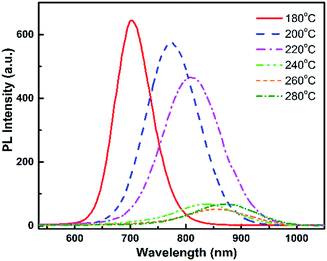
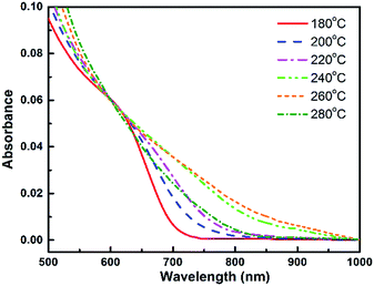
The absorption spectra of this sample series show that there is a change in absorption intensity and edge when nanocrystal growth temperature is increased (Fig. 2). The absorption edge is shifted towards longer wavelengths for higher growth temperature, in agreement with the PL spectra. Thus, the absorption capability of QDs fabricated at 240 °C to 260 °C increases notably in the NIR region. The absorption and emission wavelengths are in the same range as values previously reported by Bailey et al.,4 but redshifted with respect to other samples described in.13,15,22 The photoluminescence decay curves (see ESI, Fig. SI-1†) present two characteristic times, one of 10–40 ns corresponding to the exciton radiative recombination, and the other of the order of a few nanoseconds which can be attributed to the presence of non-radiative decay channels.
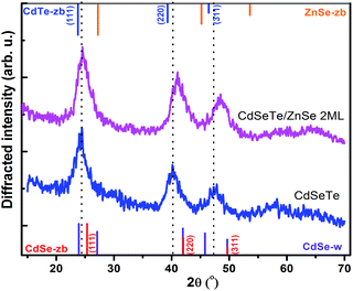
In order to analyze the reasons for the spectral shift between these different samples, we have recorded the micro-Raman spectra, XRD patterns and TEM images of all samples to obtain more information on QDs composition, shape and size.
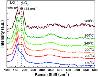
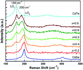
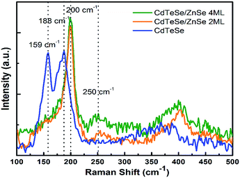
Fig. 3 displays the Raman spectra of the CdTeSe QDs samples series fabricated at different temperatures from 180 °C to 280 °C. In the frequency range of 125 and 225 cm−1, the Raman spectra have revealed CdTe-like and CdSe-like longitudinal optical (LO) phonons, labeled LO1 and LO2 respectively.
For the growth at 180 °C, only one vibration band appears at 159 cm−1 – characteristic of the CdTe-like LO mode,27,30,36 and a shoulder with lower intensity at 188 cm−1 (CdSe-like LO mode).36,37 As the growth temperature is increased, the second peak at 188 cm−1 now appears distinctly. It increases gradually and becomes equal to the peak at 159 cm−1 for 260 °C, and quite higher at 280 °C. We can conclude that the QDs synthesized at lower temperatures are CdTe-rich, due to the stronger Te reactivity, and the incorporation of Se into the QDs increases with temperature. As it was shown in ref. 38 for CdSeS quantum dots that the ratio between Raman peaks is close to the ratio between concentrations we can estimate that similar amounts of Te and Se are included in the QDs around 260 °C. Given that similar amounts of Te and Se were introduced, we interpret this as a sign that, at 260 °C, the Te and Se are incorporated into the QDs with similar efficiencies. This temperature is thus optimal in order to achieve various compositions of the CdTeSe alloy by choosing different ratios of the Se and Te reagents, as will be demonstrated in the next section.
Therefore, an increase in QD growth temperature increases their size as well as their Se concentration. The size increase leads to reduced quantum confinement and thus can explain the observed redshifted luminescence at higher growth temperature. The higher Se concentration also contributes to this redshift (note that, due to the optical bowing effect, adding a small amount of Se to CdTe leads to a luminescence redshift although CdSe has a higher bandgap energy than CdTe). As explained previously, the growth temperature of 260 °C will be chosen as it allows the best incorporation of both Te and Se into the alloy QDs. The PL efficiency was found to decrease above 240 °C, however further characterizations (see discussion in ESI, Fig. SI-5 and SI-6†) showed that significantly higher PL efficiencies could be obtained, especially at high temperatures, without changing the resulting Se![[thin space (1/6-em)]](https://www.rsc.org/images/entities/char_2009.gif) :
:![[thin space (1/6-em)]](https://www.rsc.org/images/entities/char_2009.gif) Te composition and its dependence of temperature, by removing the OLA ligand from the precursor solution. We will use this modified protocol in the following.
Te composition and its dependence of temperature, by removing the OLA ligand from the precursor solution. We will use this modified protocol in the following.
Effect of the change of the Te/Se precursors ratio
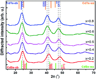
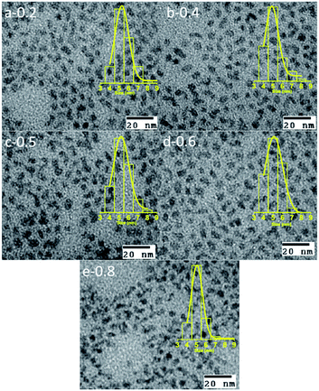
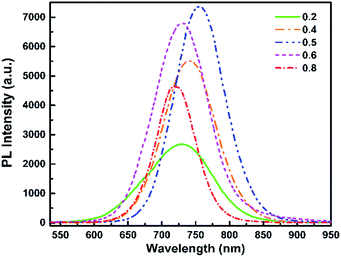
We now consider the second CdTeSe QD samples series fabricated at 260 °C for 10 min, with only the Te/(Te + Se) precursors ratio (x) changed at values of x = 0, 0.2, 0.4, 0.5, 0.6, 0.8 and 1. We examine whether the Se![[thin space (1/6-em)]](https://www.rsc.org/images/entities/char_2009.gif) :
:![[thin space (1/6-em)]](https://www.rsc.org/images/entities/char_2009.gif) Te composition of the QDs can be tuned, while keeping other parameters (QD size) constant.
Te composition of the QDs can be tuned, while keeping other parameters (QD size) constant.
Study on the alloyed CdTeSe/ZnSe QDs
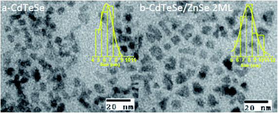
We finally consider a series of CdTeSe samples fabricated at 260 °C with x = 0.5 and shelled with a ZnSe layer of different thicknesses. Two samples were considered for more detailed studies: CdTeSe cores and CdTeSe shelled with ZnSe 2 ML nominal thickness.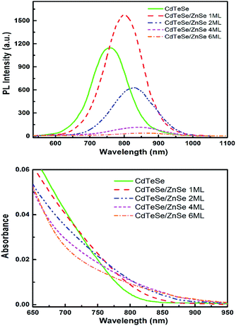 | ||
| Fig. 11 Photoluminescence (top) and absorption (bottom) spectra of the CdTeSe and CdTeSe coated with shells of ZnSe with different monolayer thicknesses (nML, n = 1, 2, 4 and 6). | ||
The absorption edge of CdTeSe QD cores is located at 820 nm wavelength, and is shifted towards longer wavelengths – by 50 nm when coated with a ZnSe layer 2 ML thick, and 8 nm when coated a layer ZnSe layer 6 ML thick. The absorption band expanding up to ∼900 nm is an interesting feature for applications in solar cells. This redshift might be related to a penetration of the charges into an additional CdSe layer, although CdSe has a larger band gap; an increase of the Se concentration in the CdTeSe alloy would also lead to a blueshift, as shown in Fig. 9. A possible explanation for the large redshift could be the appearance of a type-II structure in these QDs, which would also explain the relatively long radiative decay time observed on single QDs (see Fig. 13 below). Further analysis, for instance HR-TEM imaging of the QDs, would be necessary in order to elucidate this aspect, which is important as NIR absorption and slow radiative decay are key elements for photovoltaic applications.
Single-QD optical properties
We now use a microphotoluminescence setup to analyze the luminescence of individual CdTeSe/ZnSe quantum dots. Fig. 12 (left) shows the PL intensity autocorrelation curve (distribution of delays between one photon and the next photon detected) of a typical emitter under excitation by a pulsed laser with 400 ns pulse repetition period. The peaks at times multiples of 400 ns indicate that all photons are emitted slightly after a laser pulse so that the delay between two photons is roughly a multiple of 400 ns. The nearly-perfect absence of a peak at zero delay indicates that there is never emission of two photons following the same laser pulse. This indicates that for these CdTeSe/ZnSe nanocrystals we have obtained single-photon emission, most likely because multi-exciton emission is quenched by Auger effect. The minor residual peak might be due to self-luminescence from the substrate, possibly with a slight contribution from multi-exciton emission.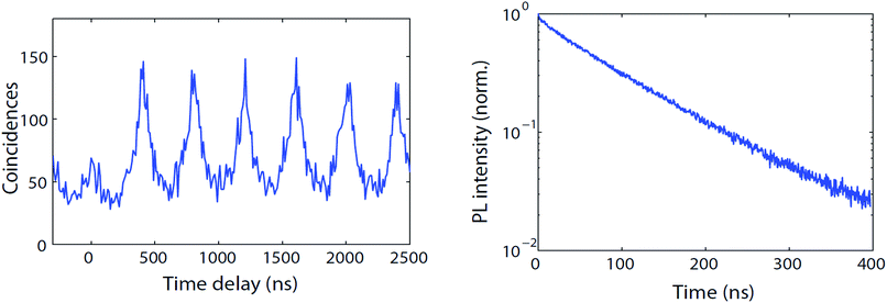 | ||
| Fig. 12 Left: PL intensity autocorrelation g(2) function (arb. units) of a typical individual CdTeSe quantum dot. Right: Decay curve (norm.) of the same quantum dot. | ||
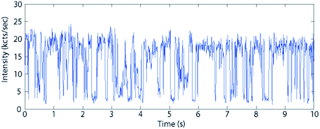
Fig. 12 (right) plots the decay curve of the same quantum dot. This curve is remarkably close to a mono-exponential, with an unusually long decay time of 110 ns. This observation, which was reproduced for all single quantum dots observed with similar 110 ± 15 ns decay times, is in contrast with ensemble measurements, possibly because the latter are performed at much higher power which could excite multi-excitonic or other non-radiative recombination pathways (the increase of multi-excitonic contribution upon shell growth could then be explained by decreased competition with Auger decay). Under the single-QD observation conditions, there is no (fast) multiexcitonic contribution and, during the measurement (100 seconds), there were very few fluctuations of the decay time. This excellent stability is confirmed by considering the intensity variations of a typical quantum dot (Fig. 13). Some non-fluorescent periods (“off”) are observed, but they constitute only 20% of the total time (and less than 10% for many other QDs). During the “on” periods, the emission remains remarkably stable.
Conclusions
In summary, CdTeSe QDs with up to 860 nm emission bands have been fabricated. The absorption intensity of these QDs starts to become stronger at wavelengths ∼850 nm when fabricated at 260 °C. The QDs crystallize stably at CdTeSe zinc-blende phase at the growth temperature of 260 °C. The NIR absorbing properties at NIR make CdTeSe QDs usable in solar cells. Raman scattering spectra can be used as a powerful tool to evaluate qualitatively the amount of Te:Se in the alloy CdTeSe QDs. When the nanocrystal growth temperature is increased, their size increases as well as the amount of Se in the QDs. When the amount of Te reagent is increased, the intensity of the CdTe-like LO line increases compared to that of the CdSe-like LO line in CdTeSe QDs, showing increased Te concentration in the QD – the QD size, on the other hand, can be kept constant. Upon growth of a ZnSe shell, the emission band is redshifted up to 900 nm. For single core–shell nanocrystals, perfect single-photon emission is obtained, with good stability and little intermittency.Conflicts of interest
There are no conflicts to declare.Acknowledgements
This research is funded by Vietnam National Foundation for Science and Technology Development (NAFOSTED) under grant number 103.03-2014.66 and by the CNRS-VAST programm Plato (PICS 6456). P. Bassène is supported by the Service de Coopération et d’Action Culturelle of the French Embassy in Dakar. Fu Feng is supported by the ANR-12-JS04-0011 project Ponimi. The authors thank the National Key Laboratory for Electronic Materials and Devices – IMS and Duy Tan University for the use of facilities. We would like to thank Mr Pham Son Lam for his assistance in editing the paper and Prof. Vu Xuan Quang of Duy Tan University for his support.Notes and references
- R. Wang, Y. Shang, P. Kanjanaboos, W. Zhou, Z. Ning and E. H. Sargent, Energy Environ. Sci., 2016, 9, 1130–1143 CAS.
- W. W. Yu, L. Qu, W. Guo and X. Peng, Chem. Mater., 2003, 15, 2854–2860 CrossRef CAS.
- L. Li, Y. Chen, Q. Lu, J. Ji, Y. Shen, M. Xu, R. Fei, G. Yang, K. Zhang, J.-R. Zhang and J.-J. Zhu, Sci. Rep., 2013, 3, 01529 CrossRef PubMed.
- R. E. Bailey and S. Nie, J. Am. Chem. Soc., 2003, 125, 7100–7106 CrossRef CAS PubMed.
- J. Xue, X. Chen, S. Liu, F. Zheng, L. He, L. Li and J. J. Zhu, ACS Appl. Mater. Interfaces, 2015, 7, 19126–19133 CAS.
- H. Zou, M. Liu, D. Zhou, X. Zhang, Y. Liu, B. Yang and H. Zhang, J. Phys. Chem. C, 2017, 121, 5313–5323 CAS.
- J. Yang, J. Wang, K. Zhao, T. Izuishi, Y. Li, Q. Shen and X. Zhong, J. Phys. Chem. C, 2015, 119, 28800–28808 CAS.
- Z. Du, Z. Pan, F. Fabregat-Santiago, K. Zhao, D. Long, H. Zhang, Y. Zhao, X. Zhong, J. S. Yu and J. Bisquert, J. Phys. Chem. Lett., 2016, 7, 3103–3111 CrossRef CAS PubMed.
- S. K. Verma, R. Verma, N. Li, D. Xiong, S. Tian, W. Xiang, Z. Zhang, Y. Xie and X. Zhao, Sol. Energy Mater. Sol. Cells, 2016, 157, 161–170 CrossRef CAS.
- G. Wang, H. Wei, Y. Luo, H. Wu, D. Li, X. Zhong and Q. Meng, J. Power Sources, 2016, 302, 266–273 CrossRef CAS.
- R. Soltania, A. A. Katbaba, K. Schaumbergerb, N. Gasparinib, C. J. Brabec, S. Rechbergerd, E. Spieckerd, A. G. Alabaue, A. Rulandf, A. Sahag, D. M. Guldig, V. Sgobba and T. Ameri, J. Mater. Chem. C, 2017, 5, 654–662 RSC.
- X. Zhong, M. Han, Z. Dong, T. J. White and W. Knoll, J. Am. Chem. Soc., 2003, 125, 8589–8594 CrossRef CAS PubMed.
- Z. Pan, K. Zhao, J. Wang, H. Zhang, Y. Feng and X. Zhong, ACS Nano, 2013, 7(6), 5215–5222 CrossRef CAS PubMed.
- W. Jiang, A. Singhal, J. Zheng, C. Wang and W. C. W. Chan, Chem. Mater., 2006, 18, 4845–4854 CrossRef CAS.
- T. Pons, N. Lequeu, B. Mahler, S. Sasnousk, A. Fragola and B. Dubertret, Chem. Mater., 2009, 21, 1418–1424 CrossRef CAS.
- B. Xing, W. Li, X. Wang, H. Dou, L. Wang, K. Sun, X. He, J. Han, H. Xiao, J. Miao and Y. Li, J. Mater. Chem., 2010, 20, 5664 RSC.
- R. Wang, O. Calvignanello, C. I. Ratcliffe, X. Wu, D. M. Leek, M. B. Zaman, D. Kingston, J. A. Ripmeester and K. Yu, J. Phys. Chem. C, 2009, 113, 3402–3408 CAS.
- Z. Wan, W. Luan and S. T. Tu, J. Colloid Interface Sci., 2011, 356, 78–85 CrossRef CAS PubMed.
- L. Song, J. Duan and J. Zhan, Mater. Lett., 2010, 64, 1843–1845 CrossRef CAS.
- L. X. Hung, P. N. Thang, H. Van Nong, N. H. Yen, V. Đ. Chinh, L. Van Vu, N. T. T. Hien, W. D. de Marcillac, P. N. Hong, N. T. Loan, C. Schwob, A. Maître, N. Q. Liem, P. Bénalloul, L. Coolen and P. T. Nga, J. Electron. Mater., 2016, 45, 4425–4431 CrossRef CAS.
- T. Debnath, S. Maiti and H. N. Ghosh, J. Phys. Chem. Lett., 2016, 7, 1359–1367 CrossRef CAS PubMed.
- L. Liu, X. Xu, T. Luo, Y. Liu, Z. Yang and J. Lei, Solid State Commun., 2012, 152, 1103–1107 CrossRef CAS.
- L. Liao, H. Zhang and X. Zhong, J. Lumin., 2011, 131, 322–327 CrossRef CAS.
- F. Yang, Z. Xu, J. Wang, F. Zan, C. Dong and J. Ren, Luminescence, 2013, 28, 392–400 CrossRef CAS PubMed.
- H. Y. Nguyen, W. D. de Marcillac, C. Lethiec, N. H. Phan, C. Schwob, A. Maître, Q. L. Nguyen, V. V. Le, P. Bénalloul, L. Coolen and P. Thu Nga, Opt. Mater., 2014, 36, 1534–1541 CrossRef CAS.
- J. D. Poplawsky, W. Guo, N. Paudel, A. Ng, K. More, D. Leonard and Y. Yan, Nat. Commun., 2016, 7, 12537 CrossRef CAS PubMed.
- V. Dzhagan, I. Lokteva, C. Himcinschi, X. Jin, J. Kolny-Olesiak and D. R. Zahn, Nanoscale Res. Lett., 2011, 6, 79 CrossRef PubMed.
- S. Li, G. Tan, J. B. Murowchick, C. Wisner, N. Leventis, T. Xia, X. Chen and Z. Peng, J. Electron. Mater., 2013, 42, 3373–3378 CrossRef CAS.
- B. T. Spann and X. Xu, Appl. Phys. Lett., 2014, 105, 083111 CrossRef.
- Z. Chai, W. Wu, D. Kong, Y. Gao and Q. Chang, J. Non-Cryst. Solids, 2013, 382, 121–124 CrossRef CAS.
- D. N. Talwar, Z. C. Feng, J.-F. Lee and P. Becla, Phys. Rev. B: Condens. Matter Mater. Phys., 2013, 87, 1652018 CrossRef.
- E. S. F. Neto, S. W. da Silva, P. C. Morais, M. I. Vasilevskiy, M. A. Pereira-da-Silva and N. O. Dantas, J. Raman Spectrosc., 2011, 42, 1660–1669 CrossRef.
- S. Perkowitz, L. S. Kim and P. Becla, Phys. Rev. B: Condens. Matter Mater. Phys., 1991, 43, 6598–6601 CrossRef CAS.
- D. N. Talwar, T.-R. Yang, Z. C. Feng and P. Becla, Phys. Rev. B: Condens. Matter Mater. Phys., 2011, 84, 174203 CrossRef.
- H. W. Verleur and J. A. S. Barker, Phys. Rev., 1966, 149, 715–729 CrossRef CAS.
- V. S. Vinogradov, G. Karczewski, I. V. Kucherenko, N. N. Mel’nik and P. Fernandez, Phys. Solid State, 2011, 50, 164–167 CrossRef.
- A. V. Bragas, C. Aku-Leh and R. Merlin, Phys. Rev. B: Condens. Matter Mater. Phys., 2006, 73, 125305 CrossRef.
- P. Mukherjee, S. J. Lim, T. P. Wrobel, R. Bhargava and A. M. Smith, J. Am. Chem. Soc., 2016, 138, 10887–10896 CrossRef CAS PubMed.
- V. M. Dzhagan, M. Y. Valakh, A. E. Raevskaya, A. L. Stroyuk, S. Y. Kuchmiy and D. R. T. Zahn, Nanotechnology, 2007, 18, 285701 CrossRef.
- V. M. Dzhagan, M. Y. Valakh, O. E. Raevska, O. L. Stroyuk, S. Y. Kuchmiy and D. R. Zahn, Nanotechnology, 2009, 20, 365704 CrossRef CAS PubMed.
Footnote |
| † Electronic supplementary information (ESI) available. See DOI: 10.1039/c7ra06500k |
| This journal is © The Royal Society of Chemistry 2017 |

