
 Open Access Article
 This Open Access Article is licensed under a
 Creative Commons Attribution 3.0 Unported Licence
Systematic tuning of segmented magnetic nanowires into three-dimensional arrays of ‘bits’†
S. Bochmanna,
A. Fernandez-Pachecob,
M. Mačkovićc,
A. Neffd,
K. R. Siefermannd,
E. Spieckerc,
R. P. Cowburnb and
J. Bachmann *a
*a
aFriedrich-Alexander University of Erlangen-Nürnberg, Inorganic Chemistry, Egerlandstrasse 1, 91058 Erlangen, Germany. E-mail: julien.bachmann@fau.de
bCavendish Laboratory, University of Cambridge, J. J. Thomson Avenue, Cambridge CB3 0HE, UK
cInstitute of Micro- and Nanostructure Research (WW9), Center for Nanoanalysis and Electron Microscopy (CENEM), Cauerstr. 6, 91058 Erlangen, Germany
dLeibniz Institute of Surface Modification (IOM), Permoserstrasse 15, 04318 Leipzig, Germany
First published on 31st July 2017
Abstract
A method is presented for the preparation of a three-dimensional magnetic data storage material system. The major ingredients are an inert nanoporous matrix prepared by anodization and galvanic plating of magnetic and non-magnetic metals in wire shape inside the cylindrical pores. The individual nanomagnets consist of a nickel–cobalt alloy, the composition of which is tuned systematically by adjusting the electrolytic bath composition at one optimal applied potential. The lowest magnetocrystalline anisotropy is obtained at the composition Ni60Co40, as quantified by superconducting quantum interference device magnetometry. Wires of this composition experience a pinning-free propagation of magnetic domain walls, as determined by single-wire magneto-optical Kerr effect magnetometry. Adding copper into the electrolyte allows one to generate segments of Ni60Co40 separated by non-magnetic copper. The segment structure is apparent in individual nanowires imaged by scanning electron microscopy, UV-photoelectron emission microscopy, and transmission electron microscopy. The single-domain structure of the wire segments is evidenced by magnetic force microscopy.
Introduction
Current magnetic data storage devices (computer hard drives) rely on a two-dimensional (2D) design. The lower limit of bit size, defined by the transition from ferromagnetic to superparamagnetic behavior as particles are reduced in size, combined with the 2D design, currently prevents magnetic data storage from keeping up with other storage media in terms of density, speed, and energy efficiency.1 A possible strategy for exploiting the third dimension of space in magnetic data storage was proposed based on the so-called ‘racetrack’ concept.2 Indeed, if parallel arrays of ‘vertically’ arranged nanowires were used, the areal storage density could be increased by several orders of magnitude despite the lower limit on bit size. Since such wires would need to be embedded in some non-magnetic matrix, however, individual bits would be buried in the bulk of the matrix, instead of being accessible at the surface directly. Therefore, the read/write technique must rely on the motion of domain boundaries along the wires in order to render the information accessible. To date, however, this concept has not been transferred into devices on an applicable scale.Several individual aspects pertaining to the racetrack memory have been addressed. On the one hand, much has been investigated on domain wall motion induced by spin-polarized electrical current and/or magnetic fields in thin stripes serving as model systems, generated mostly by lithographic methods.3–5 In those studies, lithography enables the experimentalist to define any designer shape, in particular arbitrarily arranged notches or other geometric features serving to define a unitary step size of the domain wall motions. From the preparative viewpoint, however, this approach is limited to 2D objects and cannot be applied towards a 3D system. In another large set of studies, parallel arrays of ‘vertical’ nanowires have been generated in a truly three-dimensional fashion, mostly by galvanic methods in an inert template.6–8 The magnetic properties of such wires have been characterized, in part as they depend on geometry and material composition.9–13 In a smaller subset of those studies, segments of ferromagnetic and diamagnetic metals have even been combined in nanowires.14–16 This strategy of introducing a structure along the wires' length by alternating two distinct metals (instead of defining notches) would enable one to exploit solitons in order to code information,17 whereby the magnetic sections would switch sequentially, propagating data vertically by means of RKKY or dipolar interactions in a cascade-like manner.18–20
What has been missing to date is the demonstration that a materials system can be prepared that simultaneously combines all of the following features, necessary for the realization of any type of 3D magnetic memory based on the motions of solitons:
(1) Wires must be defined which run parallel to each other and which combine segments of two metals, one ferromagnetic and one diamagnetic, grown from the same one electrolytic bath.
(2) The wire diameter must be below 100 nm (approximately, depending on the physical parameters of the ferromagnetic material) in order to favor a single-domain behavior of the ferromagnetic segments laterally.
(3) For lateral distances between wires on the order of 50 to 500 nm, the relative amount of ferromagnetic material inside the matrix must be significantly below 10% (approximately, depending on the physical parameters) in order to prevent significant dipolar interactions between neighboring wires.
(4) The ferromagnetic material must have tunable physical properties, in particular low magnetic anisotropy (sum of magnetocrystalline and shape anisotropies) in order to control its magnetic state via the wire shape.
(5) The wire diameter and individual segment lengths must be tunable.
(6) The segments of two materials must serve to define the step size for soliton motion, and each individual segment must be sufficiently homogeneous and smooth to prevent undesired domain wall pinning in the middle of a segment.
For each of these six features considered individually, the literature provides precedents; their combination in a single system, however, which is required for the generation of a practically exploitable three-dimensional magnetic memory, has not been possible to date. The present paper introduces a preparation of segmented NixCoy/Cu wires which addresses these aspects in a systematic manner and demonstrates them simultaneously.
Results and discussion
Growth parameters of NixCoy wires
We choose macroporous ‘anodic’ alumina as a template system, as it enables one to generate parallel pores with diameters and lengths tunable between 20 nm and 300 nm and between 0.5 μm and 100 μm approximately, respectively.6 We also choose nickel–cobalt as a ferromagnetic alloy phase in which the composition can be varied continuously from pure Ni to pure Co and the magnetic behavior changes from soft to hard accordingly.9 In this section, the goal is to find conditions for the uniform growth of smooth wires, that is, the growth rate must be well defined and uniform across the whole macroscopic sample, and the wire surface must display minimal roughness.Starting with a cobalt sulfate/cobalt chloride/boric acid electrolyte with saccharin as a “brightener”, or smoothing agent,20 the first observation is that an optimal deposition potential exists. At an applied potential of −1.10 V vs. Ag/AgCl, the metallic cobalt wires exhibit the lowest roughness and most uniform length (Fig. 1b). At −1.00 V, the quality is considerably lower, with significant roughness and non-uniform length (Fig. 1a). We note that the contrasting results obtained at −1.00 V and −1.10 V are highly reproducible, whereas saccharin does significantly improve the quality of the wires, all other parameters being maintained constant. Upon addition of nickel (in form of sulfate and chloride) to the electrolyte, the results at −1.10 V remain best (Fig. 2). Since the potential will be varied later in order to define the segments of NixCoy and Cu, the NixCoy composition must be tuned solely based on the ratio of Ni2+ and Co2+ ions in the electrolyte.
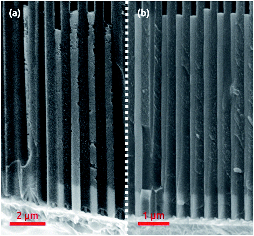 | ||
| Fig. 1 Co nanowires of 300 nm diameter grown inside the porous template at an applied potential of −1.0 V (a) and −1.1 V (b) vs. Ag/AgCl. The latter value results in smoother, more uniform wires. A thin sputtered Au film and short Au segment subsequently grown (galvanically) as the electrical contact are observable near the lower extremity of the pores. | ||
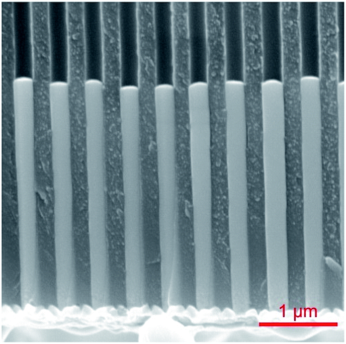 | ||
| Fig. 2 NiCo nanowires of 300 nm diameter deposited inside the porous template at −1.1 V vs. Ag/AgCl. | ||
Fig. 3 displays the composition of the solid deposited at the potential −1.10 V as a function of the electrolyte composition, whereby the total concentration of Co2+ and Ni2+ ions is maintained at 0.32 M. The data are obtained by atomic absorption after complete dissolution of the solid samples to minimize the experimental uncertainty (≤0.1%). The dependence is not a straight line with unity slope due to the distinct aqueous chemistries of Ni2+ and Co2+, whereas the electrochemical potentials are very similar (E°(Ni) = −0.46 V, E°(Co) = −0.49 V vs. Ag/AgCl).21 However, any desired NixCoy alloy can be obtained at the sole potential of −1.10 V.
 | ||
| Fig. 3 Composition of the NiCo wires (diameter 300 nm) deposited, determined by atomic absorption spectroscopy (AAS), as a function of the electrolyte composition. | ||
Magnetic tuning of NixCoy wires
The magnetic properties of wires deposited in pores of 300 nm diameter depend on their composition in a sensitive and non-linear manner. Fig. 4 compares the magnetic hysteresis loops recorded by SQUID magnetometry on Ni60Co40 (blue) and Ni42Co58 (purple) as an example. The shapes of the loops for the two materials are distinct, and they also depend on the magnetic field orientation with respect to the wire axis, a manifestation of magnetic anisotropy present in the samples, as well as the different dipolar interactions for both configurations. Fig. 5a quantifies the composition effect on anisotropy by summarizing the coercive field (Hc) values extracted from the SQUID loops for a series of NixCoy alloy wire samples (in the alumina matrix) held with the wire axis parallel to the applied magnetic field (squares) and perpendicular to it (triangles). Pure Ni and pure Co wire samples are also displayed for comparison. The graph is similar if remanence values are plotted (instead of Hc) as a function of the composition (Fig. S1 in the ESI†).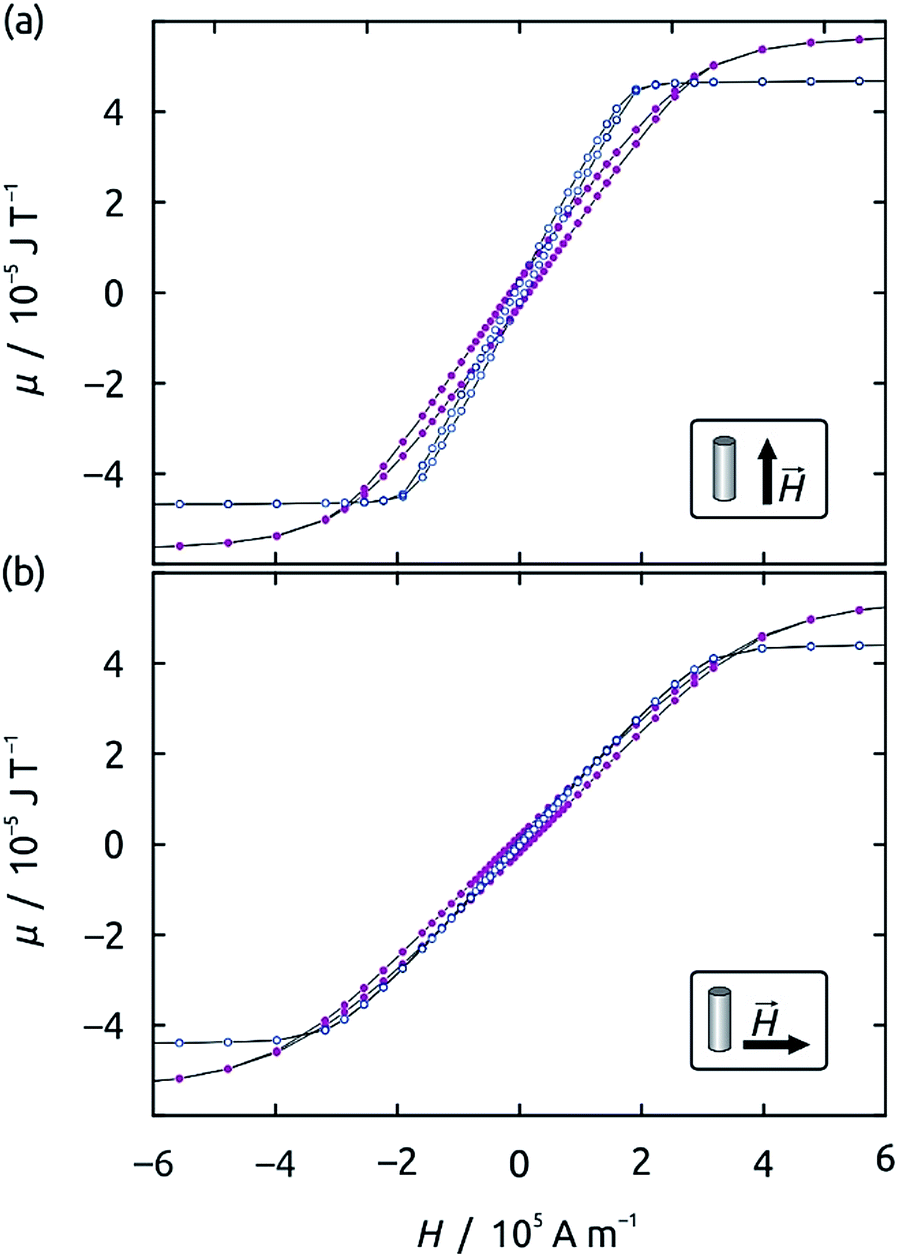 | ||
| Fig. 4 Magnetic hysteresis curves obtained for Ni60Co40 (empty blue circles) and Ni42Co58 (full purple disks) wires of 300 nm diameter by SQUID magnetometry with the external field applied either parallel to the wires' long axis (a) or perpendicular to it (b). | ||
 | ||
| Fig. 5 Structural and magnetic properties of NixCoy wires (300 nm diameter) of various compositions. (a) Coercive field values recorded on the same samples by SQUID magnetometry with the wires' long axis oriented parallel to the applied field (triangles) and perpendicular to it (squares). The softest sample (green: large shape anisotropy, small Hc perpendicular) has the hcp phase with the least Ni. (b) X-ray diffractograms recorded on five different sample compositions. The positions of the most prevalent peaks of the Co hcp and Ni fcc phases are highlighted in red and green, respectively. | ||
Pure Co nanowires give rise to almost identical Hc values in both orientations. This effect may be caused by the magnetocrystalline anisotropy of hcp cobalt, which can result into similar magnetic loops if the crystals are large enough and randomly oriented.7,22 On the other extremity of the spectrum, pure Ni wires display a significantly different coercivity for both field orientations. This is consistent with the soft magnetic behavior of the metal, related with its highly symmetric cubic (fcc) structure.23,24 However, the absolute values of Hc are still large for spintronic application. Mixing Ni into Co initially increases Hc values, but beyond 25% Ni a beneficial effect appears, in that not only does Hc decrease again, but a difference also becomes observable between both orientations, indicating that a soft magnetic alloy with shape anisotropy dominating its magnetic behavior. The ideal composition is Ni60Co40: here, a very low coercive field value of Hc = 1090 A m−1 (13 Oe) is obtained in the perpendicular orientation (hard magnetization axis), and the ratio between both Hc values reaches a factor of 7. Additionally, the remanence for fields applied along the hard axis becomes close to zero. The reason for these observations is apparent when the crystal structures of the various samples are compared (X-ray diffraction, Fig. 5b). The Co-rich compositions (<25% Ni) yield wires in the undesired magnetically hard hcp phase (characterized by the peaks at 41° and 47°), the Ni42Co58 sample displays an fcc structure with a broad peak at 51°, and from Ni60Co40 on, the fcc crystal is well established.
Further insight into the intrinsic magnetic properties of the wires is obtained by spatially resolved magneto-optical Kerr effect (MOKE) magnetometry of an isolated Ni60Co40 wire removed from the template in chromic acid solution (Fig. 6a). The hysteresis loop measured in parallel configuration yields a switching field of 11![[thin space (1/6-em)]](https://www.rsc.org/images/entities/char_2009.gif) 800 A m−1 (148 Oe), slightly larger than the coercive field determined in the matrix 7480 A m−1 (94 Oe), which can be explained by the lack of antiferromagnetic dipolar coupling between the wires when embedded in the matrix. Importantly, the switching is perfectly abrupt after averaging 250 individual loops. This rules out any substantial domain wall pinning or stochastic nucleation behavior.25 This type of magnetic behavior, similar for instance to the one characteristic of permalloy, is desired for many magnetic applications. This is to be contrasted to the situation of the less soft composition Ni82Co18 (Fig. 6b), where a slanted slope is observed between both saturation levels, indicating either domain wall pinning or stochastic nucleation processes, which result in a gradual switching overall after averaging.
800 A m−1 (148 Oe), slightly larger than the coercive field determined in the matrix 7480 A m−1 (94 Oe), which can be explained by the lack of antiferromagnetic dipolar coupling between the wires when embedded in the matrix. Importantly, the switching is perfectly abrupt after averaging 250 individual loops. This rules out any substantial domain wall pinning or stochastic nucleation behavior.25 This type of magnetic behavior, similar for instance to the one characteristic of permalloy, is desired for many magnetic applications. This is to be contrasted to the situation of the less soft composition Ni82Co18 (Fig. 6b), where a slanted slope is observed between both saturation levels, indicating either domain wall pinning or stochastic nucleation processes, which result in a gradual switching overall after averaging.
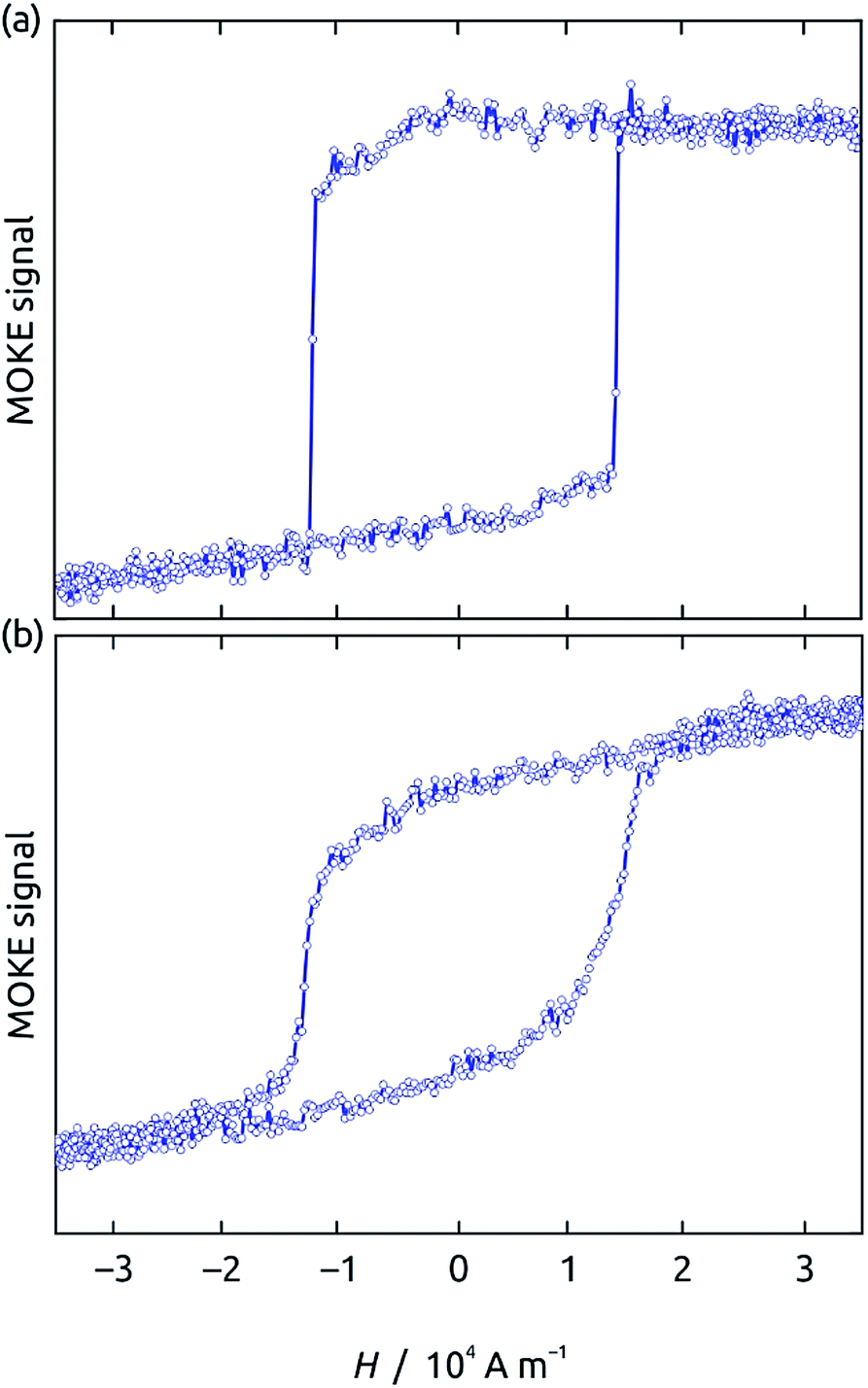 | ||
| Fig. 6 Magnetic hysteresis loops recorded by magneto-optical magnetometry (MOKE) on individual wires of 300 nm diameter and composition (a) Ni60Co40 and (b) Ni82Co18. The switching is perfectly abrupt with the softest composition (a) and more gradual for less optimal materials (b). The vertical axis is in arbitrary units: in MOKE magnetometry, a signal proportional to the local magnetization is recorded as a polarized light intensity. | ||
Segmented NixCoy/Cu wires
Copper metal is chosen as the diamagnetic spacer between the ferromagnetic bits as it is immiscible with Co.26,27 The deposition of NixCoy/Cu segments necessitates a ternary electrolyte. Chloride, needed as a brightener,28–30 is already present in the NixCoy bath. Since the redox potential of Cu2+/Cu is significantly more positive (E°(Cu) = +0.13 V vs. Ag/AgCl) than those of Ni2+/Ni and Co2+/Co, the Cu2+ salt must be much more dilute in order to minimize co-deposition of Cu into NixCoy, and the Cu segments must be grown at a less negative potential. We choose 10 mM CuSO4 (a 32-fold dilution with respect to Ni2+ + Co2+) and a deposition potential of −0.4 V. In those conditions, we obtain a growth rate of approximately 400 nm min−1 for NixCoy and 50 nm min−1 for Cu. Atomic absorption (AAS) measurements reveal that in those conditions, Ni60Co40 is magnetically diluted by the inclusion of 12% Cu, whereas conversely (and expectedly based on the less negative deposition potential), the Cu obtained from the ternary electrolyte contains ≤0.1% Ni and Co. The Ni:Co ratios determined from those samples are identical to those presented in Fig. 3 within experimental uncertainty.
Fig. 7a shows a segmented Ni60Co40/Cu nanowire with individual segment lengths set to 1 μm isolated from the alumina matrix by chromic acid etching. The corresponding X-ray microanalysis trace (EDX, Fig. 7b) reveals the expected alternation of Cu and Ni/Co signals. The signal quantification is in agreement with the AAS data (Fig. S2 in ESI†). If instead of chromic acid (which passivates metal surfaces), sodium hydroxide is used to dissolve the matrix, the Cu segments are partly dissolved, so that an alternating contrast is obtained in electron microscopy, enabling one to also observe shorter segments clearly: Fig. 7c and d display wires with 200 nm individual segment length and a total of more than 200 segments treated in this manner. A view of a bundle of many segmented nanowires after removal of the matrix is provided in ESI (Fig. S3†).
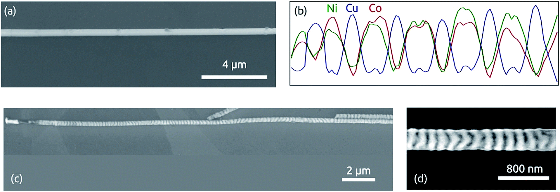 | ||
| Fig. 7 Segmented NiCo/Cu nanowires of 300 nm diameter. (a) Scanning electron micrograph (SEM) of one wire isolated from the matrix with chromic acid. (b) Corresponding X-ray microanalysis (EDX) displaying segments of 1 μm length each (quantification: Fig. S2†). (c) SEM of one wire isolated from the matrix with sodium hydroxide. (d) High-magnification view of the sample wire displaying segments of 200 nm each. | ||
Photoemission electron microscopy (PEEM) furnishes another method to image segmented nanowires without the need for a destructive treatment of the sample.31 Fig. S4† displays the micrograph of an isolated nanowire imaged with ultraviolet-PEEM. The wire is of the same type as those shown in Fig. 7c and d, but was isolated from the matrix with chromic acid (instead of sodium hydroxide) which leaves the wires intact. The alternating segments of length 200 nm are observable due to the differences of NiCo and Cu with regard to the band structure near the Fermi energy.32 We note that PEEM offers an ultimate lateral resolution of <40 nm. In combination with a polarized light source, PEEM might even allow one to image the orientation of individual domains in a contactless fashion. Key to such measurements is the magnetic dichroism of photoemission.33,34
The application of such segmented wires to magnetic data storage necessitates thinner wires than those shown up to this point (with 300 nm diameter). For this, macroporous anodic alumina prepared in oxalic acid (instead of phosphoric acid) can be used.6 We have found that despite possibly more stringent mass transport limitations during electrodeposition in the narrower pores, all preparative procedures described above can be transferred to pores of 40 nm diameter without adjustment. Fig. 8 demonstrates the success of this transfer by atomic force microscopy of an isolated Ni60Co40/Cu.
 | ||
| Fig. 8 Structural characterization of thin (40 nm diameter), segmented NiCo/Cu wires isolated from the matrix. Atomic force micrograph of a straight segment, investigated by magnetic force microscopy in Fig. 11. | ||
The excellent material quality and segmented nature of such thin Ni60Co40/Cu nanowires is further proven by transmission electron microscopy (TEM, Fig. 9). The exemplary bright-field TEM images in Fig. 9a and b show two crystallites along the nanowire, one composed of NiCo, the other of Cu, each appearing with darker contrast upon individual tilting in Bragg condition. The corresponding convergent beam electron diffraction (CBED) patterns in Fig. 9c and d obtained from the areas marked by white dotted circles in a and b establish the single-crystalline, face-centered cubic (fcc) and hexagonal close-packed (hcp) crystal structure of Cu and NiCo, respectively. As can be further seen from the TEM bright-field images (Fig. 9a and b), other crystallites along the nanowire show a high density of stacking faults and twins. We further performed a detailed high angle annular dark field (HAADF) scanning TEM (STEM) analysis in combination with energy-dispersive X-ray (EDX) spectroscopy, in order to obtain a local distribution of the individual elements/phases in the nanowires. These results are shown in Fig. 10 and S5† for two individual nanowires. EDX mappings confirm the alternation of NiCo and Cu segments along the nanowires, separated by sharp transition. The hcp nature of the Ni60Co40 segments observed here stands in contrast to the results presented in Fig. 5b, obtained on pure NixCoy wires. It results from the addition of copper(II) to the electrolytic bath, as demonstrated by a comparative XRD study of Ni60Co40 wires grown from a Ni(II)/Co(II) electrolyte, Ni60Co40 wires grown from the Ni(II)/Co(II)/Cu(II) electrolyte, and segmented Ni60Co40/Cu wires grown from the Ni(II)/Co(II)/Cu(II) electrolyte (Fig. S6 in the ESI†).
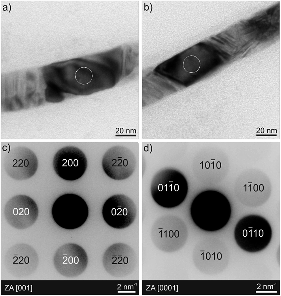 | ||
| Fig. 9 Representative TEM results of Ni60Co40/Cu nanowire of 40 nm diameter. The bright-field TEM images in (a and b) show crystallites in different sections of one nanowire. The corresponding (contrast inverted) CBED patterns in (c and d) are obtained from the nanowire segments with darker contrast in (a and b), and correspond to the [001] zone axis of fcc Cu (ICSD 43493) and to the [0001] zone axis of hcp NiCo (ICSD 102567), respectively. | ||
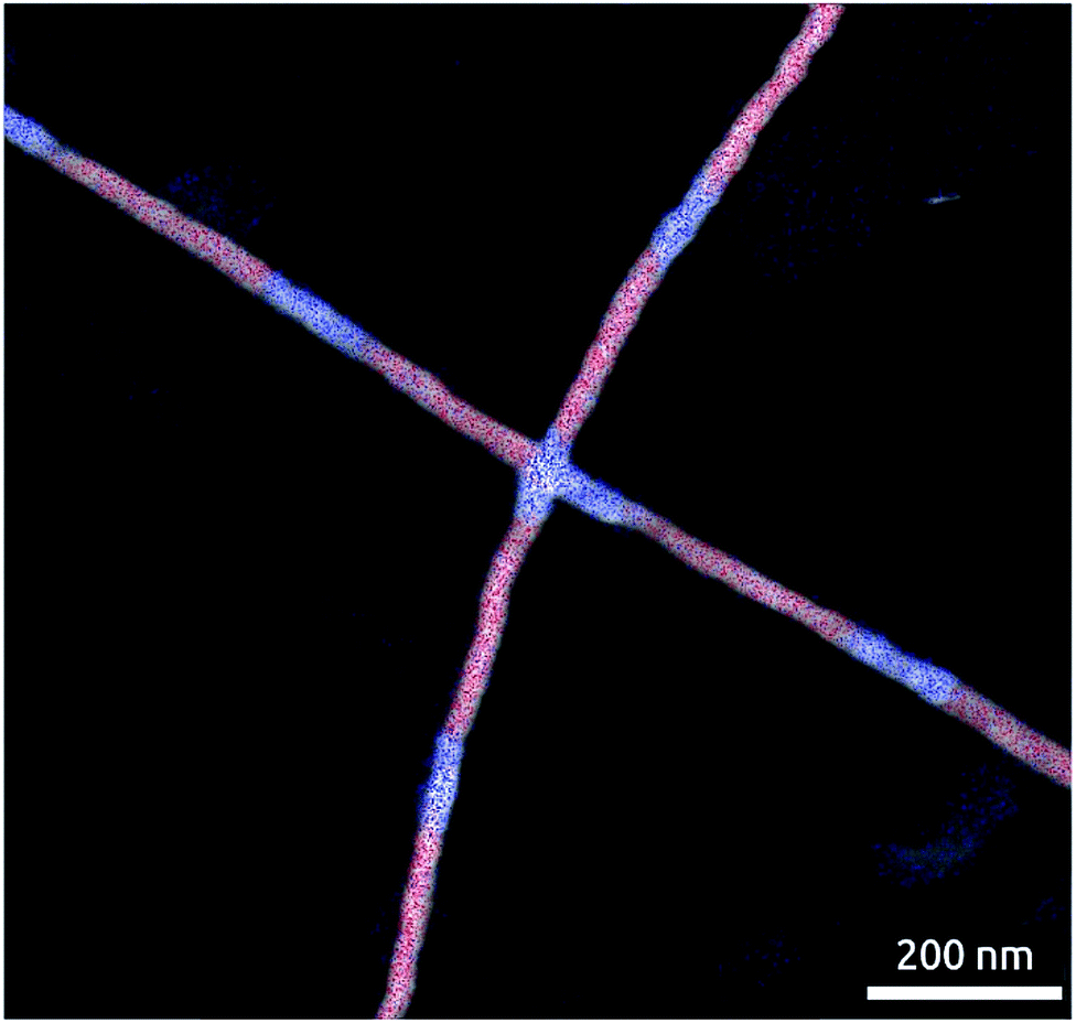 | ||
| Fig. 10 HAADF-STEM image superimposed with elemental maps showing the local distribution of Co (red) and Cu (blue) in Ni60Co40/Cu nanowires of 40 nm diameter. Individual EDX maps of the elements Ni, Co and Cu are presented in Fig. S5.† | ||
The final demonstration of our preparative method's success must be a functional characterization. Fig. 11 presents a magnetic force micrograph (MFM) of an isolated Ni60Co40/Cu wire with 40 nm diameter, prepared by repeating 0.5 min growth at −1.1 V and 4.0 min at −0.4 V. This corresponds to individual segments of 200 nm each. The presence of well-defined segments is visualized immediately. To interpret the micrograph further, we remind the reader that MFM contrast mirrors a derivative of the vertical component of the stray field generated by magnetized material.35 Thus, volumes of solid magnetized homogeneously in the horizontal plane appear identical to non-magnetic solid, except at their extremities, where the presence of magnetic charges concentrates the stray field lines. Our wire in Fig. 11 does exhibit the dark and white extremities expected of a wire magnetized parallel to its axis. Additionally, the alternation of dark and white contrast along the wire length is due to the individual Ni60Co40 segments, which are single domains (Fig. 11). Thus, the distance between two consecutive white spots represents one Ni60Co40/Cu alternation. The wire observed in Fig. 11 has a total length of approximately 4.78 μm for 23 individual segments—which yields an individual segment length of almost exactly 200 nm, as designed. While Fig. 11 is similar to literature data in an absolute sense, its originality lies in the fact that it represents a few individual elements from a three-dimensional array of single-domain bits made of soft magnetic material, ordered with a density of approximately 3.4 Terabits per square inch (3.4 Tbit per in2, based on the hexagonal geometry with 105 nm pitch and a 40 μm total pore length). This figure lies significantly beyond the current commercial state of the art of 1.3 Tbit per in2.
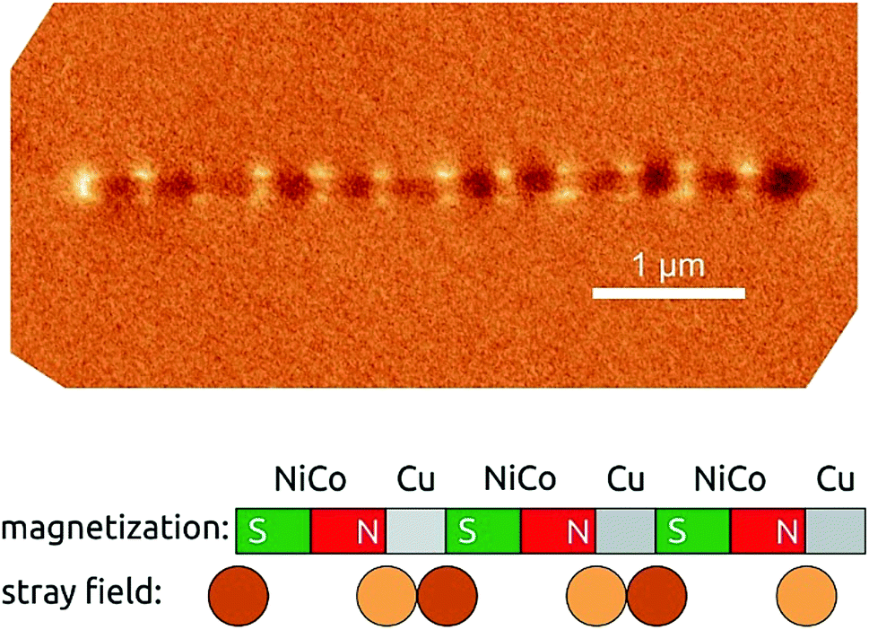 | ||
| Fig. 11 Top, magnetic force micrograph of an isolated Ni60Co40/Cu wire of 40 nm diameter (shown in Fig. 8). Lower panel, schematic representation of how the pattern observed in MFM originates from the alternation of magnetized and non-magnetic segments. | ||
Conclusions
We report a galvanic preparative method that allows for the preparation of long nanowire arrays formed by alternating Co and Ni. The ternary Ni2+/Co2+/Cu2+ electrolyte introduced here enables one to switch between NixCoy and Cu based on the applied potential, and to tune the composition of the NixCoy material based on the electrolyte solely. This system simultaneously fulfills all of the following conditions required for three-dimensional magnetic data storage applications:(1) The parallel order of wires is defined by the anodic alumina template and bits are defined by ferromagnetic NixCoy, and separated by diamagnetic Cu.
(2) Wires can be thin (40 nm) to prevent the appearance of undesired multidomain magnetic structures. The growth method does not change from 300 nm to 40 nm wire diameter.
(3) With a 1:1 NixCoy/Cu segment length ratio and with a 105 nm pitch of the hexagonal arrangement of parallel wires, ferromagnetic material only amounts to 6% of the total volume, which given the saturated magnetization of Ni60Co40 ensures low dipolar interactions.
(4) The NixCoy system is highly tunable via its composition, from hard-magnetic and shape-insensitive (Co-rich) to soft-magnetic and highly shape anisotropic (Ni60Co40).
(5) The wire diameter is tunable based on anodization conditions (at least between 40 nm and 300 nm) and individual segment lengths are tunable from few nanometers to microns in proportionality to deposition duration.
(6) The Cu segments are shown to generate very well-defined individual Ni60Co40 magnets (by MFM), whereas the smooth and crystalline Ni60Co40 material enables for a pinning-free propagation of domain walls (as shown by MOKE magnetometry).
While each individual one of those features had already been achieved previously, the present work is the first demonstration of their combination in one single material system. Our methods allow, for the first time, that magnetic data storage bits be designed and prepared in large three-dimensional arrays with structural and physical quality parameters compatible with competitive storage schemes. We are currently working on magnetoresistive elements embedded in the middle of the segmented NixCoy/Cu wires in order to read/write bits within each wire, a requirement needed towards an actual three-dimensional storage device.
Experimental procedures
As the template for the galvanic preparation of ordered, cylindrical nanowires we used anodic alumina providing pores of various diameters (40–400 nm). Aluminium (0.5 mm, 99.99%, Smart Membranes) was anodized in two steps on a home-made setup.36 The aluminum was first electropolished with HClO4 in ethanol (1:3 vol.) at +20.0 V for 5 min. Anodization was then performed either with 0.3 M oxalic acid a potential of +40 V or 1% phosphoric acid and a potential of +195 V. The first anodization was performed for 24 h, the second anodization was carried out for either 8 h or 30 h. After removing the remaining aluminum metal with a mixture of CuCl2·2H2O (13.6 g, 79.8 mM), HCl (37%, 100 mL), and 400 mL H2O, the barrier layer was removed with phosphoric acid. After sputtering (Torr CRC 622) a thin metallic layer as the electrical contact onto the free-standing membrane (50 nm Au for templates anodized in phosphoric acid, and 6 nm Al + 50 nm Au for those anodized in oxalic acid), then a short Au segment of wire was grown in a two-electrode configuration under −2.5 V from an aqueous KAu(CN)2 (5.0 g L−1)/(NH4)2SO4 (0.2 M) bath set to pH 7. Subsequently, electrodepositions were performed in a three-electrode electrochemical cell, with an Ag/AgCl/NaCl (3 M) electrode as the reference electrode. NiCo nanowires were grown from electrolytic baths with compositions summarized in Table 1. The pH was adjusted to 2.5. NiCo/Cu wires were grown from ternary electrolytes based on those of Table 1 with 10.0 mM CuSO4 added. For NiCo/Cu, the deposition used potential switching between −0.4 V for Cu and −1.1 V for NiCo layers (vs. Ag/AgCl).
| c/mM | 8.2% | 15.3% | 31.0% | 46.5% | 64.5% |
|---|---|---|---|---|---|
| CoSO4 | 27.5 | 45 | 90 | 130 | 180 |
| CoCl2 | 2.5 | 5.0 | 10 | 20 | 20 |
| NiSO4 | 290 | 240 | 190 | 140 | 100 |
| NiCl2 | 52.5 | 40 | 30 | 30 | 20 |
| H3BO3 | 500 | 500 | 500 | 500 | 500 |
| Saccharin | 15 | 15 | 15 | 15 | 15 |
For atomic absorption spectroscopy (Shimadzu AA-7000F) the nanowires were dissolved in 10 mL aqua regia. Magnetometry has been performed at 5 K on a SQUID MPMS-XL magnetometer from Quantum Design. Scanning electron micrographs were taken on a Jeol JSM 6400. PEEM measurements were performed with an IS-PEEM (FOCUS GmbH) under ultrahigh vacuum conditions (<10–9 mbar) using an Hg lamp for illumination at grazing incidence (25° to sample surface). 5 μL of a nanowire suspension were drop-casted onto a Si wafer under normal air atmosphere. After evaporation of the solvent, the sample was introduced into the PEEM instrument. For the measurements presented here, the extractor voltage was set to 12 kV at a working distance of 1.8 mm. Acquisition time was 10 s per image, whereas Fig. 8 shows the averaged result of 5 images. MOKE measurements were performed in a NanoMOKE2 system by Durham Magnetooptics, with a laser diameter of 5 μm. The measurements were carried out at room temperature, with magnetic fields applied at 27 Hz. The setup was configured in a longitudinal configuration, probing the magnetization parallel to the optical plane and in the substrate plane. MFM measurements were performed in a Veeco Multimode system at zero fields. We used commercial MESP tips from Bruker, with Cobalt–Chromium coatings for magnetic imaging. TEM was performed by using a Philips CM30 TWIN/STEM equipped with a LaB6 cathode and operated at 300 kV acceleration voltage. TEM images and electron diffraction patterns are obtained by using a fast-scan charged coupled device camera from TVIPS (Tietz Video and Image Processing Systems GmbH) with an image size of 1024 × 1024 pixels. Further TEM analysis was performed by using a Titan3 Themis equipped with a high-brightness field-emission gun (X-FEG), a monochromator system, two CS-correctors (probe and image size), a Super-X detector for EDX spectroscopy, a HAADF detector and a 4k CMOS camera. The Titan3 Themis was operated at 300 kV acceleration voltage. The evaluation of the electron diffraction patterns and dynamical diffraction simulations were performed by using the software Jems (version 3.7624U2012)37 and the crystal data from the inorganic crystal structure database (ICSD). Image analysis was carried out by using the commercially available software DigitalMicrograph™ and the free available software ImageJ (version 1.46r).
Acknowledgements
We thank A. Roth for performing the atomic absorption analysis. The research leading to these results has received funding from the European Community's Seventh Framework Program under Grant No. 309589 (M3d). KRS and AN acknowledge funding from Europäischer Fonds für regionale Entwicklung (EFRE). Andreas Neff was supported by a scholarship of the Beilstein Institute. ES and MM gratefully acknowledge the financial support by the German Research Foundation (DFG) through the Cluster of Excellence EXC315 “Engineering of Advanced Materials” and the Research training group GRK1896 “In situ microscopy with electrons, X-rays and scanning probes”.Notes and references
- I. R. McFadyen, E. E. Fullerton and M. J. Carey, MRS Bull., 2006, 5, 379 CrossRef.
- S. S. P. Parkin, M. Hayashi and L. Thomas, Science, 2008, 320, 190 CrossRef CAS PubMed.
- D. A. Allwood, G. Xiong and R. P. Cowburn, Appl. Phys. Lett., 2004, 85, 2848 CrossRef CAS.
- A. Fernández-Pacheco, J. M. De Teresa, R. Córdoba, M. R. Ibarra, D. Petit, D. E. Read, L. O'Brien, E. R. Lewis, H. T. Zeng and R. P. Cowburn, Appl. Phys. Lett., 2009, 94, 192509 CrossRef.
- V. Uhlîr, S. Pizzini, N. Rougemaille, J. Novotny, V. Cros, E. Jimenez, G. Faini, L. Heyne, F. Sirotti, C. Tieg, A. Bendounan, F. Maccherozzi, R. Belkhou, J. Grollier, A. Anane and J. Vogel, Phys. Rev. B: Condens. Matter Mater. Phys., 2010, 81, 224418 CrossRef.
- K. Nielsch, J. Choi, K. Schwirn, R. B. Wehrspohn and U. Gösele, Nano Lett., 2002, 2, 677 CrossRef CAS.
- S. L. Cheng and C. N. Huang, Synth. React. Inorg. Met.–Org. Chem., 2008, 38, 475 CAS.
- B. C. Park and Y. K. Kim, Met. Mater. Int., 2017, 23, 413 CrossRef.
- V. Vega, T. Böhnert, S. Martens, M. Waleczek, J. M. Montero-Moreno, D. Görlitz, V. M. Prida and K. Nielsch, Nanotechnology, 2012, 23, 465709 CrossRef CAS PubMed.
- J. García, V. Vega, L. Iglesias, V. M. Prida, B. Hernando, E. D. Barriga-Castro, R. Mendoza-Reséndez, C. Luna, D. Görlitz and K. Nielsch, Phys. Status Solidi A, 2014, 211, 1041 CrossRef.
- A. Pereira, C. Gallardo, A. P. Espejo, J. Briones, L. G. Vivas, M. Vázquez, J. C. Denardin and J. Escrig, J. Nanopart. Res., 2013, 15, 2041 CrossRef.
- S. Talapatra, X. Tang, M. Padi, T. Kim, R. Vajtai, G. V. S. Sastry, M. Shima, S. C. Deevi and P. M. Ajayan, J. Mater. Sci., 2009, 44, 2271 CrossRef CAS.
- A. Ghemes, O. Dragos-Pinzaru, H. Chiriac, N. Lupu, M. Grigoras, D. Shore, B. Stadler and I. Tabakovic, J. Electrochem. Soc., 2017, 164, D13 CrossRef CAS.
- H. Yang, M. Zeng and R. Yu, Mater. Res. Bull., 2014, 57, 249 CrossRef CAS.
- A. Blondel, J. P. Meier, B. Doudin and J.-P. Ansermet, Appl. Phys. Lett., 1994, 65, 3019 CrossRef CAS.
- Y. P. Ivanov, A. Chuvilin, S. Lopatin and J. Kosel, ACS Nano, 2016, 10, 5326 CrossRef CAS PubMed.
- S.-L. Chin, A. Fernández-Pacheco, D. C. M. C. Petit and R. P. Cowburn, J. Appl. Phys., 2015, 118, 233905 CrossRef.
- A. Fernández-Pacheco, N. J. Steinke, D. Mahendru, A. Welbourne, R. Mansell, S. L. Chin, D. C. M. C. Petit, J. Lee, R. Dalgliesh, S. Langridge and R. P. Cowburn, Adv. Mater. Interfaces, 2016, 3, 1600097 CrossRef.
- R. Lavrijsen, J. Lee, A. Fernández-Pacheco, D. C. M. C. Petit, R. Mansell and R. P. Cowburn, Nature, 2013, 493, 647 CrossRef CAS PubMed.
- T. Osakas, T. Sawaguchi, F. Mizutani, T. Yokoshima, M. Takai and Y. Okinaka, J. Electrochem. Soc., 1999, 146, 3295 CrossRef.
- CRC Handbook of Chemistry and Physics, ed. D. R. Lide, CRC Press, Boca Raton (FL), 1992, 73rd edn, pp. 8–25 Search PubMed.
- K. R. Pirota, F. Béron, D. Zanchet, T. C. R. Rocha, D. Navas, J. Torrejón, M. Vazquez and M. Knobel, J. Appl. Phys., 2011, 109, 083919 CrossRef.
- K. Nielsch, R. B. Wehrspohn, J. Barthel, J. Kirschner, U. Gösele, S. F. Fischer and H. Kronmüller, Appl. Phys. Lett., 2001, 79, 1360 CrossRef CAS.
- K. Nielsch, R. B. Wehrspohn, J. Barthel, J. Kirschner, S. F. Fischer, H. Kronmüller, T. Schweinböck, D. Weiss and U. Gösele, J. Magn. Magn. Mater., 2002, 249, 234 CrossRef CAS.
- A. Fernández-Pacheco, L. Serrano-Ramón, J. M. Michalik, M. R. Ibarra, J. M. De Teresa, L. O'Brien, D. Petit, J. Lee and R. P. Cowburn, Sci. Rep., 2013, 3, 1492 CrossRef PubMed.
- G. R. Pattanaik, D. K. Pandya and S. C. Kashyap, Thin Solid Films, 2003, 433, 247 CrossRef CAS.
- E. Gomez, A. Labarta, A. Llorente and E. Vallés, Electrochim. Acta, 2003, 48, 1005 CrossRef CAS.
- W. H. Gauvin and C. A. Winkler, J. Electrochem. Soc., 1952, 99, 71 CrossRef CAS.
- R. E. Gana, M. G. Figueroa and R. J. Larrain, J. Appl. Electrochem., 1979, 9, 465 CrossRef CAS.
- J. W. Dini and D. D. Snyder, in Modern Electroplating, ed. M. Schlesinger and M. Paunovic, Wiley, Hoboken, NJ, 2010, ch. 2, pp. 33–79 Search PubMed.
- A. Neff, O. Naumov, T.-J. Kühn, N. Weber, M. Merkel, B. Abel, A. Varga and K. R. Siefermann, Am. J. Nano Res. Appl., 2014, 2, 27 Search PubMed.
- C. S. Fadley and D. A. Shirley, J. Res. Natl. Bur. Stand., Sect. A, 1969, 74A, 543 CrossRef.
- T. Nakagawa and T. Yokoyama, Phys. Rev. Lett., 2006, 96, 237402 CrossRef PubMed.
- C.-T. Chiang, A. Winkelmann, P. Yu and J. Kirschner, Phys. Rev. Lett., 2009, 103, 077601 CrossRef PubMed.
- S. V. Kalinin and D. A. Bonnel, in Scanning Probe Microscopy and Spectroscopy, ed. D. A. Bonnell, Wiley-VCH, NY, 2001, ch. 7, pp. 205–251 Search PubMed.
- J. Gemmer, Y. Hinrichsen, A. Abel and J. Bachmann, J. Catal., 2012, 290, 220 CrossRef CAS.
- P. Stadelmann, Java version 4.3530U2015, CIME-EPFL, Jems Electron Microscopy Software, Switzerland, 2014–2015 Search PubMed.
Footnote |
| † Electronic supplementary information (ESI) available. See DOI: 10.1039/c7ra06734h |
| This journal is © The Royal Society of Chemistry 2017 |