 Open Access Article
Creative Commons Attribution 3.0 Unported Licence
Local temperature reduction induced crystallization of MASnI3 and achieving a direct wafer production†
Zhun Yaoa,
Zhou Yang*a,
Yucheng Liua,
Wangen Zhaoa,
Xiaorong Zhanga,
Bin Liua,
Huan Wua and
Shengzhong (Frank) Liu *ab
*ab
aKey Laboratory of Applied Surface and Colloid Chemistry, National Ministry of Education, Shaanxi Engineering Lab for Advanced Energy Technology, School of Materials Science and Engineering, Shaanxi Normal University, Xi'an 710062, China. E-mail: zyang@snnu.edu.cn
bDalian National Laboratory for Clean Energy, iChEM, Dalian Institute of Chemical Physics, Chinese Academy of Sciences, Dalian, 116023, China. E-mail: szliu@dicp.ac.cn
First published on 2nd August 2017
Abstract
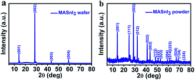
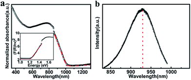
Despite the rapid advancement of perovskite solar cells, the fundamental drawback of toxicity in lead based materials has largely limited their large-scale development and application. Hence, we developed a local temperature reduction induced crystallization (LTRIC) method to directly obtain a lead-free perovskite wafer (CH3NH3SnI3), which is 110 μm-thick, in an oil bath. The XRD diffraction peaks of the MASnI3 wafer are indexed to (001) and its parallel crystal planes, demonstrating its high orientation. The UV-vis-NIR discloses that the absorption onset of the MASnI3 wafer is red-shifted to 1015 nm, corresponding to a narrow bandgap of 1.21 eV.
Introduction
Lead halide based perovskite materials have attracted tremendous attention during the past few years because of their superior optoelectronic properties such as long carrier lifetime, high carrier mobility, long carrier diffusion length, high defect tolerance, etc.1–12 Even with a lot of grain boundaries existing in the microcrystalline perovskite films, there have been several kinds of high performance optoelectronic devices developed, such as solar cells,13–15 LEDs,16 lasers,17 and photodetectors.18,19 In particular, the efficiency of the perovskite based solar cells has been increased to as high as 22.1%, approaching that of the high efficiency of crystalline silicon based solar cells.20–22To further improve performance for the optoelectronic devices, it is necessary to study defect-free single-crystalline perovskite materials.23 Single crystalline perovskite with fewer defects is the best candidate to study its intrinsic properties. Huang developed a top seed solution growth method to produce single-crystalline CH3NH3PbI3 with ultra-low trap state density (3.6 × 10 cm−3) and ultra-long carrier life time (∼90 μs) and diffusion length (>175 μm).4 Much more intriguingly, the absorption onset extended to 850 nm, around 50 nm red-shift compared to the microcrystalline films, which is better for sunlight utilization. Bakr developed an anti-solvent vapor-assisted crystallization to prepare high quality single-crystalline CH3NH3PbBr3 and CH3NH3PbI3, showing similar trap density as the Huang group reported.24 However, the carrier mobility and carrier lifetime were much smaller. Furthermore, the Bakr and Liu independently developed a high temperature induced crystallization method to produce high quality single-crystalline perovskites at high growth rate.25,26 Even though high performance photodetectors were designed and fabricated, it appears to be challenging to fabricate high efficient single-crystalline perovskite solar cells. The Bakr group used ultrasonic triggered crystallization to adjust the crystal growth process of CH3NH3PbBr3 and obtained thickness controllable single-crystalline perovskite films.27 As reported in this intriguing work, the thickness plays an important role in determining the PCEs of single-crystalline perovskite solar cells. It is predicted that only <10 μm is needed to achieve a good photovoltaic performance. The PCE of single-crystalline perovskite solar cell will decrease dramatically as the film thickness exceed 10 μm. Wafer perovskite materials were needed while most of studies to date have been limited to bulk crystals which are difficult to be implemented for optoelectronic devices.
Herein, we report development of local temperature reduction induced crystallization (LTRIC) to prepare MASnI3 wafer. The XRD results show the obtained wafer is well crystallized and shows strong orientation along [001]. MASnI3 wafer shows an extended absorption spectrum with absorption onset reaching as long as 1015 nm, exceed 150 nm longer than 850 nm of the MAPbI3 single crystal. Photoluminance (PL) peak is also red-shifted by 160 nm to 930 nm compared to MAPbI3. The great crystallinity and optical properties make the obtained wafer a good candidate to disclose its potential in optoelectronic devices.
Results and discussion
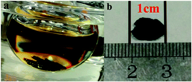
Fig. 1 shows photograph of the experimental setup and a 1 cm-sized MASnI3 wafer prepared using LTRIC method. Thin MASnI3 wafer could be found at the bottom of the precursor solution, as shown in Fig. 1a. The shape of the wafer looks like an imperfect hexagonal (Fig. 1b) that is common for general MAPbI3/MASnI3 perovskite crystals.26,28 More pictures of the MASnI3 wafers are provided in Fig. S1.†The crystallinity of the obtained MASnI3 wafer is examined using XRD. Fig. 2a shows the XRD result taken on an as-grown wafer. It is surprising to see that essentially only four diffraction peaks indexed to (001), (002), (003) and (004) crystal planes, are observed. All of the four peaks are originated from (001) and its parallel planes, indicating that the wafer is highly orientated along [001] direction. To confirm that there is no impurity phases in the wafer, XRD measurement was taken after the wafer is grounded into fine powder. There are many more additional peaks shown in Fig. 2b, all of which can be assigned to MASnI3, which agree well with the reported data (add a citation about the XRD results). Diffraction peaks from other impurity phases are not observed.
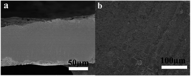
The thickness of wafer is 110 μm deduced from the cross-sectional view of wafers (seen in Fig. 3a). There are some attachments on it as shown in Fig. 3b, which makes the surface rough. That should be the reason that the wafer looks dark rather than shiny as shown in Fig. 1b.
To find out the growth mechanism, a time dependent crystal growth process has been investigated and shown in Fig. 4a–d. As shown in Fig. 4b, small dark particle would firstly form on the surface of the precursor solution and would continue growing to be a large wafer (Fig. 4c). Finally, the wafer will sink into the bulk solution because of its larger gravity than the buoyancy supported by the solvent. Then, new seed crystal will form and the wafer growth process will repeat. After carefully observing the wafer growth process, we found that small water drops condensed on the cork, which should be cooler than bulk solution, would fall off the cork and dive into the solution. The local temperature of the spot into which the drop dived is reduced. Due to the normal temperature dependent solubility of MASnI3, lowering the solution temperature will make MASnI3 solution super saturation and induce the crystallization of MASnI3. The cooled spot as we mentioned should induce the formation of MASnI3 crystal seed as observed in Fig. 4b. Based on the observation and the solubility property of MASnI3, a LTRIC process has been proposed to interpret the formation of MASnI3 wafer, as shown in Fig. 4e–i. Due to the high solvent temperature, water would evaporate quickly to form hot vapor. As the hot vapor encountered with cold cork, it would condense to a small water drop. When the water drop became larger enough, it fell off the cold cork and dropped onto the hot solution surface (Fig. 4e). The local temperature of the spot where the drop fell onto would be reduced. And the reduction in temperature could generate a driving force for perovskite crystallization because of the normal temperature dependent solubility of MASnI3. Then, small crystalline seed would be formed on the surface (Fig. 4g) as we observed during the wafer growth (Fig. 4b). Further increasing the reaction time, small seed will grow to a larger wafer, which would be sink into bulk solution as it is too heavy (Fig. 4h–j).
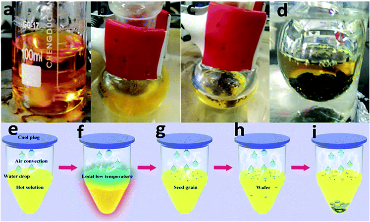 | ||
| Fig. 4 Time dependent wafer process growth (a–d) and schematic illustration of the proposed LTRIC process (e–i). | ||
To further verify our hypothesis, anhydrous diethyl ether induced crystallization of MASnI3 has been conducted as shown in Fig. S4.† First, two precursor solutions were prepared identically and immersed in 100 °C oil bath, as shown in Fig. S4a.† And the right one was used as a reference. An anhydrous diethyl ether drop was dripped into the left solution. As anhydrous diethyl ether cannot mix well with water, anhydrous diethyl ether will evaporate quickly as it contacted hot solvent surface due to its low evaporation temperature. During the evaporation, the local temperature should be reduced as evaporation process will carry energy away. Suddenly, a lot of smaller crystals were formed on the surface (Fig. S4b†). However, there is no any sign of crystal at the surface of reference solution (on the right). As the reaction process extended, a lot of wafers were formed on the surface of the solution, as shown in Fig. S4c.† At the same time, just few small crystal seeds formed at the surface of the reference solution (Fig. S4c†). That means the quick evaporation of diethyl ether anhydrous drop accelerates the crystallization of MASnI3, faster than the reference one. On the other hand, as the water on cork droplet does not easily fall off in the reference system, slower crystal formation and fewer seed crystal observed in Fig. S4c† are reasonable. Those results could be a direct prevents of our proposed LTRIC process. Cool water drop induced crystallization of MASnI3 has also been done. Shiny MASnI3 wafer can also be produced with good crystallinity, high orientation as well as much smoother surface as shown in Fig. S2 and S3.† Both of those model experiments demonstrate the local temperature reduction could be an effective way to trigger crystallization and induce direct wafer production.
The optical properties of the as grown crystals were investigated using UV-vis-NIR spectrum meter. Fig. 5a shows the UV-vis-NIR absorption spectra of the MASnI3 perovskite, whose absorption onset located at 1015 nm. UV-vis-NIR absorption spectrum of MASnI3 wafer fabricated by cool water induced crystallization is showing in Fig. S5,† which present a similar light absorption curve. The MASnI3 shows strong absorption across the entire visible spectrum and therefore it is seen as black in color. The band gap value was estimated on the basis of the Tauc plot as the intercept value of the plot of (αhν)1/m or (F(R∞)hν)1/m against photon energy hν. As MASnI3 is a direct-band gap semiconductor material, the m value is 1/2.29 By extrapolating the linear region of the (F(R∞)hν)2 30 to the energy-axis hν intercept as shown in the inset, Eg of the obtained MASnI3 can be established to be 1.21 eV, similar with the former reported value.28 The obtained MASnI3 exhibits PL peak at 930 nm as shown in Fig. 5b. It is interesting to see that the PL peak value is smaller than the absorption onsets, implying that the lights of PL due to the excitation can be extinguished by themselves. There is no doubt that it is advantageous for them to be applied in solar cells.26 Considering no PL emission being observed from solution-grown MASnI3 wafer material determination at room temperature, the PL appears to be much more prominent in the present wafer samples.
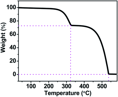
To examine the thermal stability of the perovskite MASnI3 wafer, thermogravimetric analysis (TGA) was carried out under nitrogen flow from room temperature to 570 °C with a rate of 5 °C min−1. As shown in the TGA curve (Fig. 6), the decomposition of MASnI3 could be classified to two steps, corresponding to 28% weight loss between 250 °C to 323 °C, corresponding to the CH3NH3I evaporation. 72% weight loss between 324 °C to 538 °C. The TGA result indicates the obtained MASnI3 has higher thermal stability than MAPbI3 crystal, which will be thermally decomposed at 240 °C.
Furthermore, MAPbI3 wafer has also been produced by using LTRIC method as shown in Fig. 7a. A few of MAPbI3 are floating at the surface of the solution. The XRD result of the obtained wafer is same to our previously reported results,26 demonstrating the obtained wafers are MAPbI3. Its optical absorption and emission properties were also investigated as shown in Fig. 7c and d. The wafers show strong light absorption across the whole UV-Vis-NIR region with a sharp cut-off around 830 nm and photoemission peak at 760 nm, which are similar with the reported data.
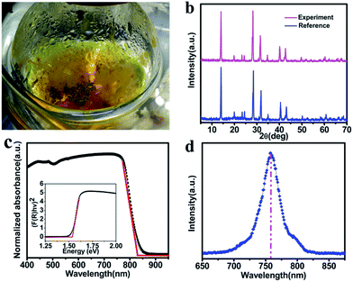 | ||
| Fig. 7 The photo, X-ray diffraction, UV-vis-NIR absorption spectrum, bandgap and PL spectra of MAPbI3 wafer. | ||
Experimental
Materials
Methylamine (CH3NH2) (40 wt% in water), hydroiodic acid (HI) (57 wt% in water, stable with 1.5 wt% hypophosphorous), and other basic materials were purchased from Sinopharm Chemical Reagent Ltd., China. PbAc2 was purchased from Xi'an Polymer Light Technology Corp. All these materials were used as received without further purification.Wafer preparation
![[thin space (1/6-em)]](https://www.rsc.org/images/entities/char_2009.gif) :
:![[thin space (1/6-em)]](https://www.rsc.org/images/entities/char_2009.gif) 1.2, as reported in literature.26 Fresh synthesized MAI (2.3850 g, 0.015 mol) and SnO (2.02 g, 0.015 mol) were dissolved in a mixed solvent of HI (30 mL) and H3PO2 (15 mL) at 80 °C. To form a transparent yellow precursor solution, the mixture was actively stirred for 8 hours. It was then transferred into a round bottom flask and submerged into an oil bath set at 100 °C. To prevent solvent evaporation, the round-bottom flask was covered with a cork. The temperature of the oil bath was slowly reduced to 98 °C in 12 h. During this process, a few small crystalline seeds were formed at the surface of the solution. As the reaction time was extended, the small seed crystals grew into larger wafers. Finally, the wafer would sink into the solution as it became bigger.
1.2, as reported in literature.26 Fresh synthesized MAI (2.3850 g, 0.015 mol) and SnO (2.02 g, 0.015 mol) were dissolved in a mixed solvent of HI (30 mL) and H3PO2 (15 mL) at 80 °C. To form a transparent yellow precursor solution, the mixture was actively stirred for 8 hours. It was then transferred into a round bottom flask and submerged into an oil bath set at 100 °C. To prevent solvent evaporation, the round-bottom flask was covered with a cork. The temperature of the oil bath was slowly reduced to 98 °C in 12 h. During this process, a few small crystalline seeds were formed at the surface of the solution. As the reaction time was extended, the small seed crystals grew into larger wafers. Finally, the wafer would sink into the solution as it became bigger.Characterization
Powder X-ray diffraction (XRD) was recorded using a DX-2700 X-ray diffract meter operated at 40 kV and 30 mA. UV-Vis-NIR diffuse reflectance spectrum was measured at room temperature using an UV-Vis-NIR spectrometer (PerkinElmer Lambda 950) with an integrating sphere attachment. A highly refined barium sulfate (BaSO4) powder plate was used as the reference (100% reflectance). The obtained reflectance data were used to estimate the band gap of the wafer by using the Kubelka–Munk equation: α/S = (1 − R)2/(2R), where α is the absorption coefficient, S the scattering coefficient, and R the reflectance.31 PL measurement was performed on a Renishaw in via Raman microscope with a 532 nm laser as excitation source. A field emission scanning electron microscopy (FE-SEM, SU-8020, Hitachi) was used to investigate the surface morphology, cross-section of the obtained wafer.Conclusions
In summary, we had successfully and directly obtained 110 μm-thick MASnI3 wafer under an ambient atmosphere by LTRIC method. After primary characterizations, it has been found that the obtained MASnI3 wafer shows good crystallinity and great orientation as well as gives a band gap of 1.21 eV, which is narrower than their corresponding thin-film material. After carefully observation and dedicated experiment design, local spot temperature reduction induced crystallization (LTRIC) has been proposed and further verified by the cold water and quick evaporation of diethyl ether anhydrous induced crystallization experiment. At the same time, MAPbI3 wafer has been successfully prepared by using this method. Our technique may provide an effective strategy for growing wafer for demanding high quality, low cost device applications. Further controlling the number of crystal seed and getting rid of surface attachment should be effective ways control the crystallization and quality of MASnI3 wafer.Acknowledgements
The authors acknowledge support from the National Key Research project MOST (2016YFA0202400/2017YFA0204800), National Natural Science Foundation of China (61674098, 61604091 and 61674098), the 111 Project (B14041), the National University Research Fund (Grant No. GK261001009, GK201603107), the Changjiang Scholar and Innovative Research Team (IRT_14R33) and the Chinese National 1000-talent-plan program (1110010341).Notes and references
- D. T. Moore, H. Sai, K. W. Tan, D. M. Smilgies, W. Zhang, H. J. Snaith, U. Wiesner and L. A. Estroff, J. Am. Chem. Soc., 2015, 137, 2350–2358 CrossRef CAS PubMed.
- M. D. McGehee, Nature, 2013, 501, 323–325 CrossRef CAS PubMed.
- H. S. Kim, C. R. Lee, J. H. Im, K. B. Lee, T. Moehl, A. Marchioro, S. J. Moon, R. Humphry-Baker, J. H. Yum, J. E. Moser, M. Gratzel and N. G. Park, Sci. Rep., 2012, 2, 591 CrossRef PubMed.
- Q. Dong, Y. Fang, Y. Shao, P. Mulligan, J. Qiu, L. Cao and J. Huang, Science, 2015, 347, 967–970 CrossRef CAS PubMed.
- D. Yang, R. Yang, J. Zhang, Z. Yang, S. Liu and C. Li, Energy Environ. Sci., 2015, 8, 3208–3214 CAS.
- X. Ren, Z. Yang, D. Yang, X. Zhang, D. Cui, Y. Liu, Q. Wei, H. Fan and S. F. Liu, Nanoscale, 2016, 8, 3816–3822 RSC.
- Y. J. Fang, Q. F. Dong, Y. C. Shao, Y. B. Yuan and J. S. Huang, Nat. Photonics, 2015, 9, 679–686 CrossRef CAS.
- J. Lee, H. F. Chen, T. Batagoda, C. Coburn, P. I. Djurovich, M. E. Thompson and S. R. Forrest, Nat. Mater., 2016, 15, 92–98 CrossRef CAS PubMed.
- Z. Lian, Q. Yan, Q. Lv, Y. Wang, L. Liu, L. Zhang, S. Pan, Q. Li, L. Wang and J. L. Sun, Sci. Rep., 2015, 5, 16563 CrossRef PubMed.
- D. H. Cao, C. C. Stoumpos, O. K. Farha, J. T. Hupp and M. G. Kanatzidis, J. Am. Chem. Soc., 2015, 137, 7843–7850 CrossRef CAS PubMed.
- D. P. McMeekin, G. Sadoughi, W. Rehman, G. E. Eperon, M. Saliba, M. T. Horantner, A. Haghighirad, N. Sakai, L. Korte, B. Rech, M. B. Johnston, L. M. Herz and H. J. Snaith, Science, 2016, 351, 151–155 CrossRef CAS PubMed.
- M. R. Filip, S. Hillman, A. A. Haghighirad, H. J. Snaith and F. Giustino, J. Phys. Chem. Lett., 2016, 7, 2579–2585 CrossRef CAS PubMed.
- M. Ibrahim Dar, M. Abdi-Jalebi, N. Arora, T. Moehl, M. Gratzel and M. K. Nazeeruddin, Adv. Mater., 2015, 27, 7221–7228 CrossRef CAS PubMed.
- D. Liu, J. Yang and T. L. Kelly, J. Am. Chem. Soc., 2014, 136, 17116–17122 CrossRef CAS PubMed.
- J. Xu, A. Buin, A. H. Ip, W. Li, O. Voznyy, R. Comin, M. Yuan, S. Jeon, Z. Ning, J. J. McDowell, P. Kanjanaboos, J. P. Sun, X. Lan, L. N. Quan, D. H. Kim, I. G. Hill, P. Maksymovych and E. H. Sargent, Nat. Commun., 2015, 6, 7081 CrossRef CAS PubMed.
- G. Wang, D. Li, H. C. Cheng, Y. Li, C. Y. Chen, A. Yin, Z. Zhao, Z. Lin, H. Wu, Q. He, M. Ding, Y. Liu, Y. Huang and X. Duan, Sci. Adv., 2015, 1, e1500613 Search PubMed.
- H. Zhu, Y. Fu, F. Meng, X. Wu, Z. Gong, Q. Ding, M. V. Gustafsson, M. T. Trinh, S. Jin and X. Y. Zhu, Nat. Mater., 2015, 14, 636–642 CrossRef CAS PubMed.
- B. R. Sutherland, A. K. Johnston, A. H. Ip, J. X. Xu, V. Adinolfi, P. Kanjanaboos and E. H. Sargent, ACS Photonics, 2015, 2, 1117–1123 CrossRef CAS.
- G. Maculan, A. D. Sheikh, A. L. Abdelhady, M. I. Saidaminov, M. A. Haque, B. Murali, E. Alarousu, O. F. Mohammed, T. Wu and O. M. Bakr, J. Phys. Chem. Lett., 2015, 6, 3781–3786 CrossRef CAS PubMed.
- W. S. Yang, B. W. Park, E. H. Jung, N. J. Jeon, Y. C. Kim, D. U. Lee, S. S. Shin, J. Seo, E. K. Kim, J. H. Nohand and S. I. Seok, Science, 2017, 356, 1376–1379 CrossRef CAS PubMed.
- V. Adinolfi, O. Ouellette, M. I. Saidaminov, G. Walters, A. L. Abdelhady, O. M. Bakr and E. H. Sargent, Adv. Mater., 2016, 28, 7264–7268 CrossRef CAS PubMed.
- J. Zhang, M.-h. Shang, P. Wang, X. Huang, J. Xu, Z. Hu, Y. Zhu and L. Han, ACS Energy Lett., 2016, 1, 535–541 CrossRef CAS.
- E. Edri, S. Kirmayer, M. Kulbak, G. Hodes and D. Cahen, J. Phys. Chem. Lett., 2014, 5, 429–433 CrossRef CAS PubMed.
- D. Shi, V. Adinolfi, R. Comin, M. Yuan, E. Alarousu, A. Buin, Y. Chen, S. Hoogland, A. Rothenberger, K. Katsiev, Y. Losovyj, X. Zhang, P. A. Dowben, O. F. Mohammed, E. H. Sargent and O. M. Bakr, Science, 2015, 347, 519–522 CrossRef CAS PubMed.
- M. I. Saidaminov, A. L. Abdelhady, B. Murali, E. Alarousu, V. M. Burlakov, W. Peng, I. Dursun, L. Wang, Y. He, G. Maculan, A. Goriely, T. Wu, O. F. Mohammed and O. M. Bakr, Nat. Commun., 2015, 6, 7586 CrossRef PubMed.
- Y. Liu, Z. Yang, D. Cui, X. Ren, J. Sun, X. Liu, J. Zhang, Q. Wei, H. Fan, F. Yu, X. Zhang, C. Zhao and S. F. Liu, Adv. Mater., 2015, 27, 5176–5183 CrossRef CAS PubMed.
- W. Peng, L. Wang, B. Murali, K. T. Ho, A. Bera, N. Cho, C. F. Kang, V. M. Burlakov, J. Pan, L. Sinatra, C. Ma, W. Xu, D. Shi, E. Alarousu, A. Goriely, J. H. He, O. F. Mohammed, T. Wu and O. M. Bakr, Adv. Mater., 2016, 28, 3383–3390 CrossRef CAS PubMed.
- Y. Dang, Y. Zhou, X. Liu, D. Ju, S. Xia, H. Xia and X. Tao, Angew. Chem., 2016, 55, 3447–3450 CrossRef CAS PubMed.
- S. Tsunekawa, T. Fukuda and A. Kasuya, J. Appl. Phys., 2000, 87, 1318 CrossRef CAS.
- L. Dimesso, M. Dimamay, M. Hamburger and W. Jaegermann, Chem. Mater., 2014, 26, 6762–6770 CrossRef CAS.
- F. Hao, C. C. Stoumpos, P. Guo, N. Zhou, T. J. Marks, R. P. Chang and M. G. Kanatzidis, J. Am. Chem. Soc., 2015, 137, 11445–11452 CrossRef CAS PubMed.
Footnote |
| † Electronic supplementary information (ESI) available. See DOI: 10.1039/c7ra07101a |
| This journal is © The Royal Society of Chemistry 2017 |

