
 Open Access Article
 This Open Access Article is licensed under a
 Creative Commons Attribution 3.0 Unported Licence
Simultaneously enhanced Jsc and FF by employing two solution-processed interfacial layers for inverted planar perovskite solar cells†
Wenhui Zhanga,
Yang Dinga,
Yue Jiang*a,
MingZhi Zhenga,
Sujuan Wua,
Xubing Lua,
Min Zenga,
Xingsen Gao a,
Qianming Wangb,
Guofu Zhouc,
Jun-ming Liud,
Krzysztof Kempaae and
Jinwei Gao*a
a,
Qianming Wangb,
Guofu Zhouc,
Jun-ming Liud,
Krzysztof Kempaae and
Jinwei Gao*a
aInstitute for Advanced Materials, Guangdong Provincial Key Laboratory of Quantum Engineering and Quantum Materials, South China Academy of Advanced Optoelectronics, South China Normal University, Guangzhou 510006, P. R. China. E-mail: gaojw@scnu.edu.cn; jiangyue871116@gmail.com
bSchool of Chemistry & Environment, South China Normal University, Guangzhou 510006, P. R. China
cElectronic Paper Displays Institute, South China Academy of Advanced Optoelectronics, South China Normal University, Guangzhou 510006, P. R. China
dLaboratory of Solid State Microstructures, Nanjing University, Nanjing 210093, P. R. China
eDepartment of Physics, Boston College, Chestnut Hill, Massachusetts 02467, USA
First published on 14th August 2017
Abstract
Interface engineering has been proved to be a practical strategy to enhance power conversion efficiency (PCE) and stability of perovskite solar cells. Recently approaches involving ultra-thin layer deposition and vacuum-processing, while improving PCE, increase the processing complexity, and thus the overall cost. In this paper, we demonstrate a high-efficiency inverted planar perovskite solar cell, obtained with a simple wet-chemistry based, room-temperature, and cost-effective process, which synthesizes two interfacial layers: solution processed molybdenum oxide (named s-MoOx) for anode and titanium(IV) oxide bis(2,4-pentanedionate) (TOPD) for cathode buffer layers. Steady-state photoluminescence (PL), time resolved photoluminescence (TRPL) and electrochemical impedance spectroscopy (EIS) are conducted to characterize the charge transport properties, confirming an enhanced charge extraction efficiency and a suppressed charge recombination. In addition, the introduction of the interfacial layers facilities formation of an ohmic contact with the metal electrode, reducing the charge transfer resistance and increasing the FF to as high as 80.7%. The optimized solar cells achieve the best PCE of 16.04% which far exceeds the PCE of devices without these interfacial layers (PCE = 11.2%).
1. Introduction
Since the first report of organometallic halide sensitized solar cells by Miyasaka et al. in 2009,1 perovskite solar cells (Per-SCs) have experienced a rapid development and shown great potential as the next-generation photovoltaic platform, owing to their excellent optical and electronic properties, including high absorption coefficient,2 low exciton binding energy,3 ambipolar charge transport,4 long electron–hole diffusion length and the solution processability.5 Until now, accompanied by the optimization in perovskite films and relevant device architectures, Per-SCs have achieved a PCE of ∼22%.6 Among them, the inverted Per-SCs (p–i–n structure), such as ITO/PEDOT:PSS/perovskite/PCBM/Ag architecture cells, are considered to be superior to the conventional n–i–p structured cells due to the simple fabrication processing, cost-effectiveness, low temperature and suppressed hysteresis.7,8 Recently, an efficient inverted perovskite solar cell with a PCE of about 20% was demonstrated.9,10Engineering of the interfacial layers, including hole or electron transport layer (ETL and HTL), blocking layer, as well as the electrode buffer layers, is critical in achieving high-efficiency inverted planar Per-SCs.11–13 Firstly, these layers can decrease the band energy offset between the active layer and the electrode, leading to the enhancement of the open circuit voltage (Voc). Secondly, the interfacial materials can also reduce the contact potential, forming the ohmic contact with electrodes, reducing the series resistance and improving the charge extraction and transport efficiency, thus lead to a higher short circuit current density (Jsc) and fill factor (FF). LiF is widely used as a cathode buffer layer between the PCBM (as an ETL) and back electrode to form a ohmic contact. However, its thickness is strictly limited to be less than 1 nm, or else significantly increases the series resistance of the device.14,15 Recently, thermally evaporated double C60 and BCP layers were investigated as interfacial layers between PCBM and the silver contact, leading to FF as high as 80.1%.16 However, expensive vacuum techniques are incompatible with the concept of low-cost fabrication of perovskite solar cells. Polymers such as PFN, PN4N etc. were used to improve the cathode interface, and resulting remarkable enhancement in PCE from 12.4% to 15.0%.17 TIPD (titanium(diisopropoxide) bis(2,4-pentanedionate)) as a cathode buffer layer has been used in Per-SCs,18 however the process of thermal annealing at 150 °C to change TIPD to TOPD,19 increases the risk of the perovskite films decomposition. Thus, a direct-processing of the TOPD in Per-SCs could be potentially a more effective way for interface improvement, which was demonstrated in organic solar cells.20
In inverted Per-SCs, PEDOT:PSS is the most commonly used HTL with a good hole transporting and collecting efficiency. However, the large band energy offset (∼0.3 eV) between PEDOT:PSS and ITO leaves the room for further improvement of Voc and the charge transfer efficiency for solar cells. Moreover, the natural acidity of PEDOT:PSS can corrode ITO, resulting in device long-term stability issue.21 Many robust materials, such as NiOx,22,23 CuOx,24 MoOx,25,26 V2O5,27 and PbS28 have been selected to replace PEDOT:PSS, while the efficiencies are lower than those of the state-of-the-art cells based on PEDOT:PSS. Recently, the MoO3/PEDOT:PSS bilayer structure was used as the HTL for inverted Per-SCs, fabricated by a vacuum deposition, showing enhanced PCE and stability.29
In this work, we used two interfacial layers: s-MoOx for anode and TOPD for cathode buffer layers in inverted CH3NH3PbI3 Per-SCs, with a simple wet-chemistry based, room-temperature, and cost-effective procession. This strategy improves the charge extraction efficiency and suppresses the charge recombination, as well as prevents ITO corrosion and forms a reduced contact potential between active layer and electrodes. The PCEs of these Per-SCs are strongly enhanced, from 11.4% (control cells) to 16.05%, mostly due to the increase of FF (from 69.2% to 80.7%) and Jsc (from 18.3% to 21.75 mA cm−2). Moreover, the PCEs of over 85% of all solar cells are higher than 14%, demonstrating good process reproducibility.
2. Experimental section
2.1. Materials and synthesis
2.2. Solar cells fabrication
ITO glasses (AGC, 11-8, 7 Ω sq−1) were patterned by laser cutting and ultrasonically cleaned with detergent, deionized water, acetone and isopropanol for 20 min, sequentially, followed by plasma cleaning for 20 min prior to use. 5 mg mL−1 of MoO2(acac)2 isopropanol solution was spin-coated at 4000 rpm for 30 s on the precleaned ITO glass, and then baked in air at 150 °C for 10 min to prepared s-MoOx film, followed by plasma cleaning for 1 min. Subsequently, PEDOT:PSS aqueous solution filtered through a 0.22 μm filter was spin-coated at 4000 rpm for 30 s on the s-MoOx film, and then baked at 120 °C in air for 15 min. Then the ITO/s-MoOx/PEDOT:PSS substrate was transferred to a nitrogen-filled glove-box for the perovskite film deposition. 461 mg of PbI2, 159 mg of CH3NH3I was dissolved in a mixed solvent of DMF and DMSO (7![[thin space (1/6-em)]](https://www.rsc.org/images/entities/char_2009.gif) :3, v/v) at 60 °C with stirring for 12 h to prepare perovskite precursor. 40 μL completely dissolved perovskite precursor solution was spin-coated on the PEDOT:PSS layer at 500 rpm for 3 s, followed by 4000 rpm for 30 s. 240 μL of chlorobenzene was quickly dripped on the rotating substrate at the beginning of 8–12 s in the second spin coating step. The substrate was immediately dried on a hot plate at 100 °C for 10 min and obtained a dense CH3NH3PbI3 film. After that, 20 mg mL−1 of PCBM solution in chlorobenzene was spin-coated at 1000 rpm for 20 s on the perovskite absorber layer. The TOPD buffer layer was prepared by spin-coating a 3 mg mL−1 TOPD isopropanol solution on the PCBM at 4000 rpm for 30 s and then stays in glove box for 24 hours for solvent annealing. The thickness of the TOPD layer was about 10 nm. Finally, Ag electrode was deposited by using thermal evaporator at a constant evaporation rate of 1 Å s−1.
:3, v/v) at 60 °C with stirring for 12 h to prepare perovskite precursor. 40 μL completely dissolved perovskite precursor solution was spin-coated on the PEDOT:PSS layer at 500 rpm for 3 s, followed by 4000 rpm for 30 s. 240 μL of chlorobenzene was quickly dripped on the rotating substrate at the beginning of 8–12 s in the second spin coating step. The substrate was immediately dried on a hot plate at 100 °C for 10 min and obtained a dense CH3NH3PbI3 film. After that, 20 mg mL−1 of PCBM solution in chlorobenzene was spin-coated at 1000 rpm for 20 s on the perovskite absorber layer. The TOPD buffer layer was prepared by spin-coating a 3 mg mL−1 TOPD isopropanol solution on the PCBM at 4000 rpm for 30 s and then stays in glove box for 24 hours for solvent annealing. The thickness of the TOPD layer was about 10 nm. Finally, Ag electrode was deposited by using thermal evaporator at a constant evaporation rate of 1 Å s−1.
2.3. Characterizations
Scanning electron microscope (SEM) images were obtained by using FE-SEM (ZEISSUltra55). Transmittance spectra were recorded with an integrating sphere system (Ocean Optics, USA) in the 400–900 nm range. X-ray diffraction (XRD) analysis was performed on a PANalytical X'Pert PRO diffractometer with the Cu-K radiation at a scan rate of 4° min−1. Steady-state PL spectra were measured using an excitation wavelength of 467 nm in an HORIBAfluorolog3. TRPL measured by Time Correlated Single Photon Counting (TCSPC, picoharp300) with a femto second laser source. J–V curves measurements were carried out using Keithley 2400 at room temperature under AM1.5G illuminations (1000 W m−2) from a solar simulator (Newport, 91160), which was calibrated using a standard silicon solar cell device by the NREL. The incident photon to converted current efficiency (IPCE) spectra was measured from 300–850 nm using a Xe source (Newport, 66902). The light intensity at each wavelength was calibrated with a standard single-crystal Si photovoltaic cell. The IPCE measurement was performed under ambient atmosphere at room temperature. EIS was measured with a CHI6601 Electrochemical Workstation with an AC signal of 200 mV in the frequency range of 0.1 Hz to 1 MHz.3. Result and discussion
Fig. 1a shows the schematic structure of the optimized inverted planar CH3NH3PbI3 Per-SC, with two interfacial layers (denoted as device C). In the structure, s-MoOx film is the anode interfacial layer above ITO electrode, and TOPD (the molecular structure in Fig. 1b) is the cathode interfacial layer between ETL and back metal contact. For comparison, two control devices, without TOPD and s-MoOx (denoted as device A) and with only TOPD (denoted as device B) have also been fabricated.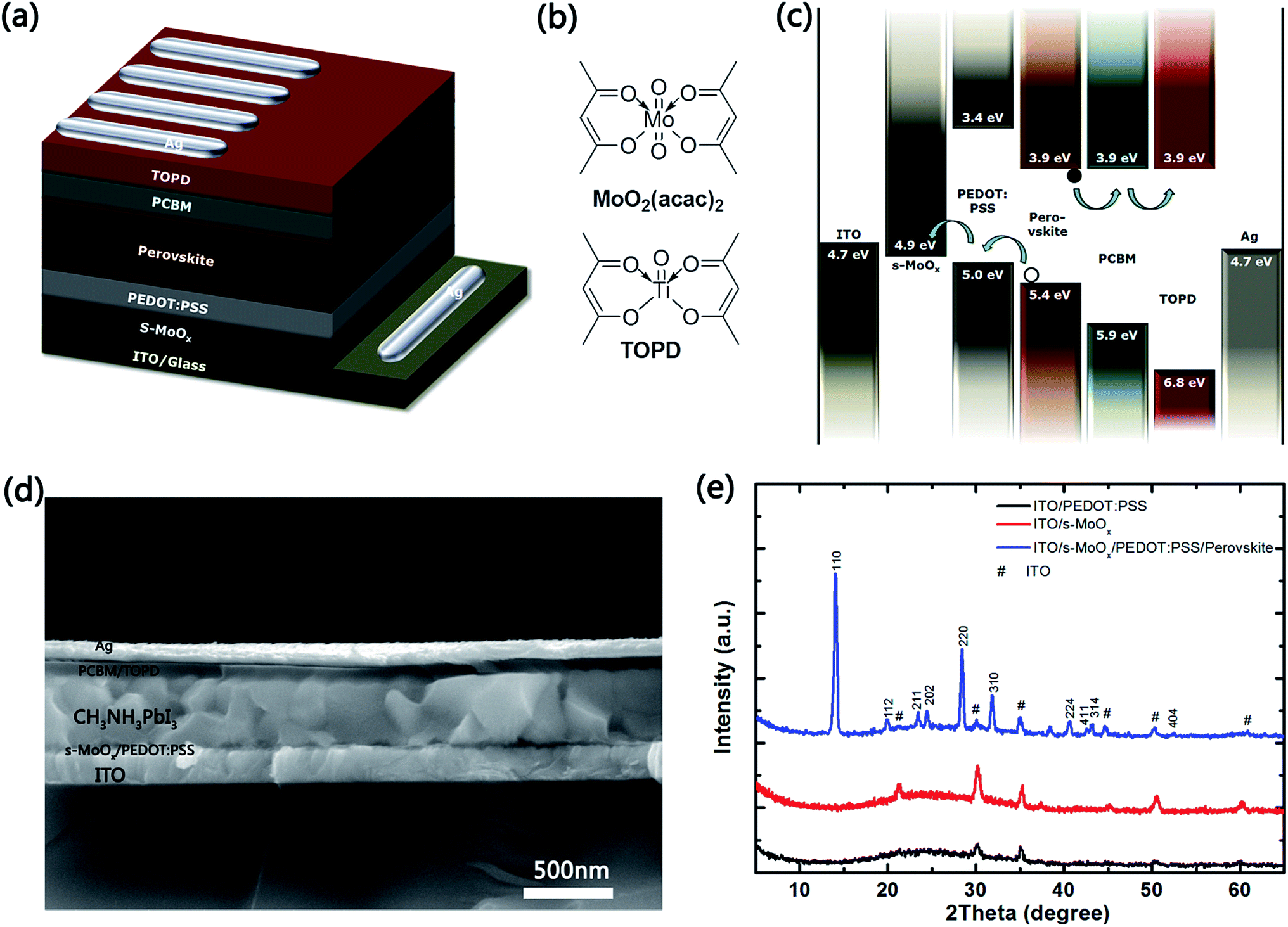 | ||
| Fig. 1 (a) Schematic architecture of optimized device C. (b) Molecular structures of MoO2(acac)2 and TOPD. (c) Schematic energy band structure of the device C. (d) Cross-section of the SEM image of the device C. (e) XRD patterns of the ITO/PEDOT:PSS, ITO/s-MoOx, and ITO/s-MoOx/PEDOT:PSS/CH3NH3PbI3. | ||
The continuous and uniform s-MoOx layer, as an anode interfacial material, was prepared according to ref. 31. Isopropanol solution of MoO2(acac)2 (the molecular structure shown in Fig. 1b) was spin-coated on the surface of pre-cleaned ITO glass, then baking in air at 150 °C for 10 min to completely transferring into s-MoOx. The obtained s-MoOx layer is highly transparent in the visible region (in Fig. S1†). The cathode interfacial layer TOPD was prepared by room-temperature spin-coating without afterwards thermal annealing. The preparation of two interfacial materials is both based on the low-temperature solution processing, which is fully compatible with flexible plastic substrate and low-cost R2R production mode. The details of solar cell fabrication are shown in Experimental section.
The band structures of the materials involve in this study, s-MoOx,31 PEDOT:PSS,12 CH3NH3PbI3,32 PCBM,12 and TOPD20 are depicted schematically in Fig. 1c. The lowest unoccupied molecular orbital (LUMO) energy level of TOPD (−3.86 eV) is very close to that of PCBM (−3.9 eV), which is favorable for electrons generated in the active layer of perovskite, and transporting from the active layer to metal electrode through TOPD. This also enhances the interfacial quality between ETL and the back contact electrode. Meanwhile its highest occupied molecular orbital (HOMO) energy level (−6.8 eV) is much lower than that of CH3NH3PbI3 (−5.4 eV), showing a strongly hole blocking capability, with bare PCBM (HOMO −5.9 eV) as an ETL. Similarly, the bottom of conduction band of s-MoOx (−4.9 eV) is close to the HOMO energy level of PEDOT:PSS (−5.0 eV), reducing the contact potential between ITO electrode and PEDOT:PSS, potentially benefiting to the hole transfer and the charge collection efficiency. In addition, both s-MoOx and TOPD interfacial materials present almost zero energy level offset comparing with other layers in devices, theoretically favoring the increase of Voc of device.
Fig. 1d shows the cross-section scanning electron microscopy (SEM) of optimized device C, with double interfacial layers. A well-defined, layer-by-layer structure with clear interfaces can be observed. The thicknesses of s-MoOx, PEDOT:PSS, CH3NH3PbI3, PCBM, and TOPD are about 10, 30, 430, 50, and 10 nm, respectively. The CH3NH3PbI3 film was uniform and the grain size in the vertical direction is comparable to or even larger than the whole film size, remarkably reducing the defects in the grain boundaries. This indicates that the photo generated charge carriers can effectively transport across a single crystal of the CH3NH3PbI3 films and reach the corresponding charge-carrier extraction interfaces before recombination. Fig. 1e shows the X-ray Diffraction (XRD) patterns of s-MoOx, PEDOT:PSS, and s-MoOx/PEDOT:PSS/CH3NH3PbI3 films deposited on ITO glass. The patterns of ITO/PEDOT:PSS and ITO/s-MoOx only present a series of ITO characteristic peaks, illustrating an amorphous phase of PEDOT:PSS and s-MoOx, which agrees with the ref. 29 and 31. The main diffraction peaks of 2θ at 14.02°, 28.4°, and 31.84° correspond to the (110), (220) and (310) planes of CH3NH3PbI3 respectively, indicating a pure standard tetragonal crystal structure.33,34
The current density–voltage (J–V) characteristics curves (under one sun illumination of AM1.5G, 100 mW cm−2) of device C, as well as control cells of A, B, are shown in Fig. 2a, and the detailed photovoltaic parameters are summarized in Table 1. The control device A shows a PCE of 11.4%, with a Jsc of 18.3 mA cm−2, a Voc of 0.88 V and a FF of 69.2%. Device B, exhibits an improved PCE of 14.35%, with a Jsc 20.97 mA cm−2, a Voc of 0.86 V and a FF of 79.4%. Comparing to A, the PCE of device B has been increased more than ∼25%. This could be ascribed to the enhanced FF (∼15%) due to the introduction of TOPD interfacial layer and lowering the series resistance. Device C, optimized with two interfacial layers (TOPD in cathode and s-MoOx in anode) leads to a further remarkable enhancement in Jsc from 20.97 to 21.75 mA cm−2, Voc from 0.86 to 0.914 V, and FF from 79.4% to 80.7%, achieving a highest PCE of 16.04%. Due to the well-matched energy levels, as well as effective electrons and holes extraction from CH3NH3PbI3 layer, device C shows significant enhancement in Jsc (∼18%) and FF (∼16%) comparing to device A. Moreover, a higher Voc was obtained in device C due to the smallest bandgap offset. The incident photon to converted current efficiency (IPCE) spectra of the corresponding devices (A, B, and C) is shown in Fig. 2b. Device C, presenting a broad plateau of ∼80% in the region from 350 nm to 750 nm, shows a higher intensity than those of device B (∼75%) and A (∼70%). The integrated Jsc from the IPCE spectra are 18.28 mA cm−2, 20.13 mA cm−2 and 21.25 mA cm−2 for device A, B, and C, respectively, in agreement with the results obtained from J–V measurement mentioned above.
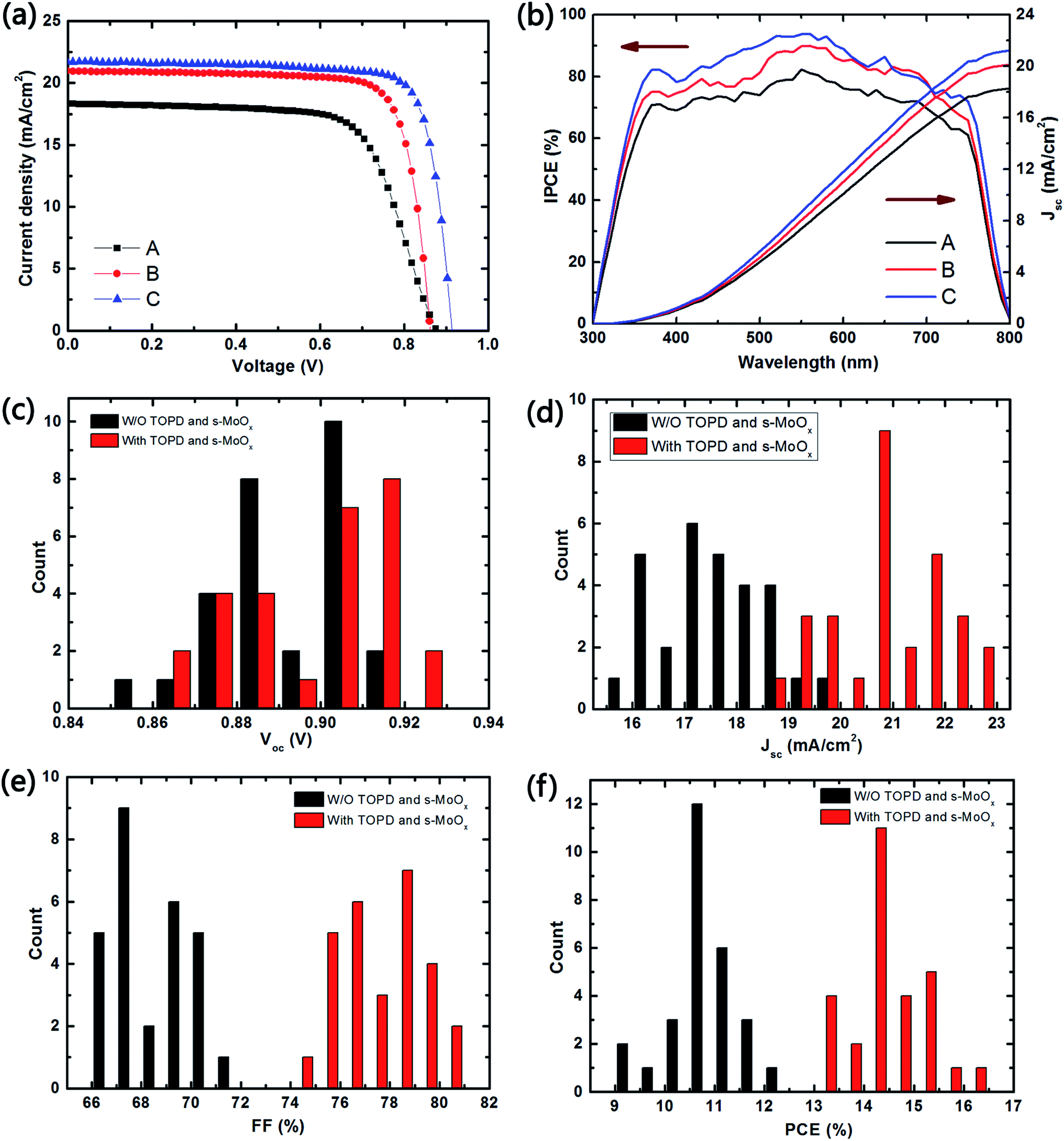 | ||
| Fig. 2 Photovoltaic performance of devices. (a) J–V curves for devices (A–C) at reversed scan, under one sun illumination of AM1.5G, 100 mW cm−2 (b) IPCE spectra (left) with integrated Jsc (right) based on IPCE measurement. Distribution histograms of Voc (c), Jsc (d), FF (e), and PCE (f) of the 28 independently fabricated devices. | ||
| Device# | Voc (V) | Jsc (mA cm−2) | FF (%) | PCE (%) |
|---|---|---|---|---|
| (A) W/O s-MoOx and TOPD | 0.88 | 18.30 | 69.2 | 11.4 |
| (B) With TOPD | 0.86 | 20.97 | 79.4 | 14.35 |
| (C) With s-MoOx and TOPD | 0.91 | 21.75 | 80.7 | 16.04 |
The statistics of the Jsc, Voc, FF and PCE for 28 independently devices A and C are shown in Fig. 2c–f. The detailed parameters for all cells are shown in Table S1.† Statistical distribution of Voc (0.90 V) for device C is slightly higher than that of device A (0.89 V), whereas its Jsc and FF (20.89 mA cm−2 and 77.5%) are remarkably larger than that of device A (17.54 mA cm−2 and 68.6%). Most importantly, the PCEs of over 85% of device C are higher than 14%, demonstrating the good reproducibility of the high-performance Per-SCs with s-MoOx and TOPD as interfacial layers. The hysteresis in the J–V curves of device C has been studied at different scan rate (0.14–1.4 V s−1) and opposite scan directions (Fig. S2†). Those curves, both in different scan rates and opposite directions present almost the same, demonstrating that there is no obvious photocurrent hysteresis for the optimized device C.
To investigate the effect of s-MoOx and TOPD interfacial layers on the charge transport properties, steady-state PL spectra and TRPL were conducted and the thickness of the CH3NH3PbI3 in all films is almost fixed at an identical level. As shown in Fig. 3a, the steady-state PL intensity of the CH3NH3PbI3 film shows a strong emission peak near 770 nm, and significantly quenched after PCBM deposition. The PL intensity is completely quenched after two interfacial layers of s-MoOx and TOPD are deposited. This confirms that photo-induced carriers are more easily extracted from perovskite layer to electrode layers with the reducing charge recombination. Fig. 3b shows the TRPL for PEDOT:PSS/perovskite, PEDOT:PSS/perovskite/PCBM, PEDOT:PSS/perovskite/PCBM/TOPD and s-MoOx/PEDOT:PSS/perovskite/PCBM/TOPD deposited on the ITO substrates. The decay times were calculated to be 37.53 ns, 2.94 ns, 2.52 ns, and 1.98 ns for above four films respectively, by fitting the measured TRPL data with a bi-exponential decay function I(t)=A1e−t/1 + A2e−t/2 (the dominating lifetime is used for comparison). For the perovskite layer without a interfacial layer, the PL lifetime is about 37.53 ns. On topped by a PCBM layer, the PL lifetime quickly decreases to 2.94, which ascribes to the charge-carrier transfer from perovskite to ETL and leads to a PL intensity quenched. After imbedding the TOPD in perovskite film, the PL lifetime decreases as low as 2.52 ns. The PL life time is further reduced (1.98 ns) with introducing the s-MoOx layer on another side of the perovskite layer. This confirms that introducing of TOPD and s-MoOx layers contributes to effective PL quenching, charge-carrier transferring, and suppressing the charge recombination.
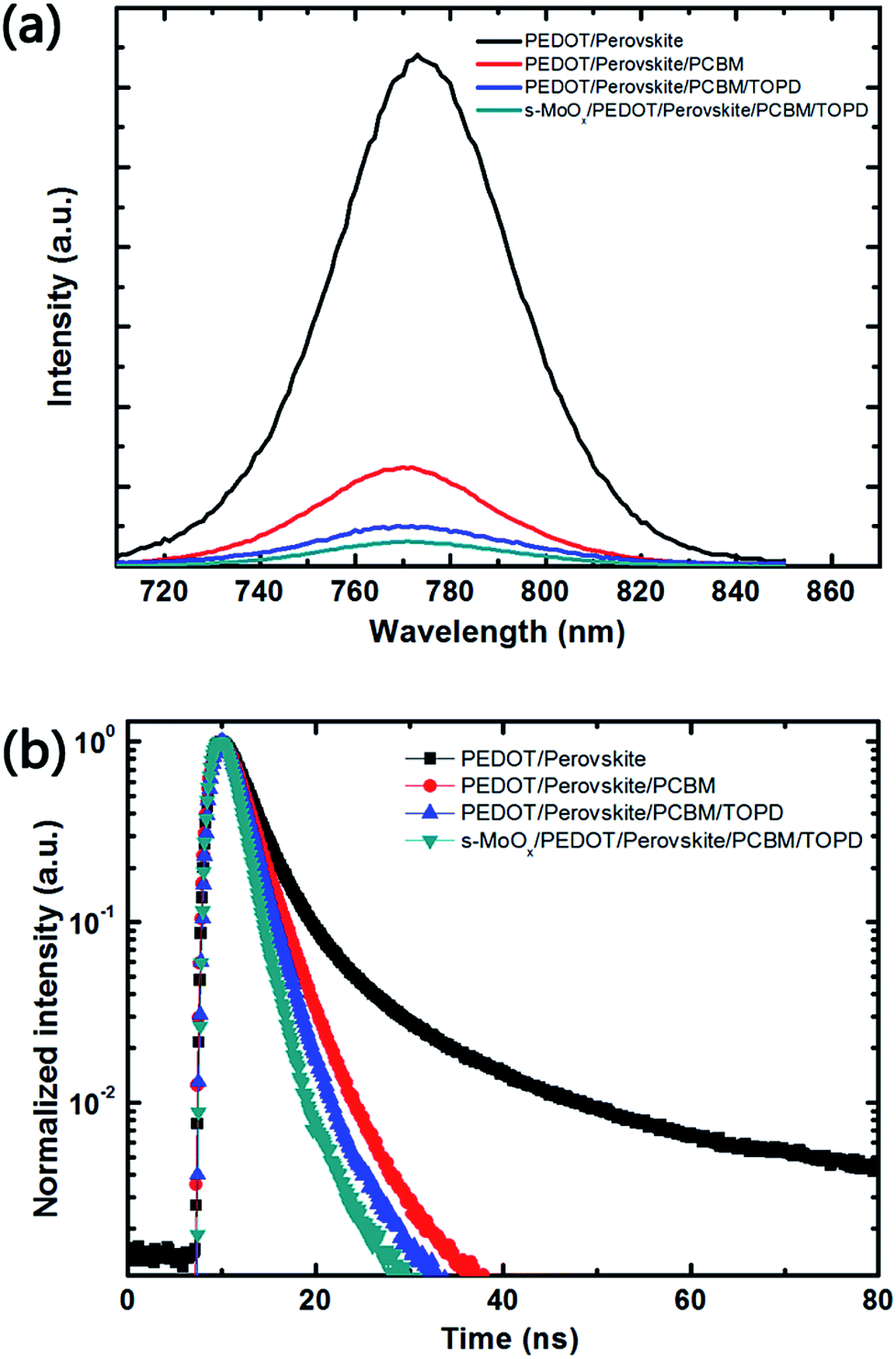 | ||
| Fig. 3 Steady state PL spectra (a) and TRPL (b) of PEDOT:PSS/perovskite, PEDOT:PSS/perovskite/PCBM, PEDOT:PSS/perovskite/PCBM/TOPD, s-MoOx/PEDOT:PSS/perovskite/PCBM/TOPD deposited on the ITO substrates. | ||
To further gain insight into the effect of s-MoOx and TOPD interfacial layers on the charge transfer resistance (Rtr) or recombination resistance (Rrec), the EIS for devices of A, B and C was carried out at 200 mV applied bias in dark condition. Fig. 4 shows the Nyquist plots of three devices (frequency range from 0.1 Hz to 100 KHz). There are two main characteristic arcs (a high frequency one and a low frequency one). We mainly study the impedance spectra at high frequency region, which related to the charge transfer resistance between perovskite film and electrodes.35 The obtained spectra were fitted to a simplified circuit model as inset shown. The transfer resistance (Rtr) is proportional to the arc size which is ranked in the sequence of A > B > C. This indicates that the insertion of both TOPD and s-MoOx interfacial layers can significantly improve the contact between active layer and electrodes and decrease the resistance of charge transfer process.
 | ||
| Fig. 4 Nyquist plots of devices A–C measured under dark ambient conditions at 200 mV applied bias. The inset shows the equivalent circuit. | ||
4. Conclusions
In conclusion, we demonstrate a high-efficiency inverted planar Per-SC by introducing two interfacial layers, s-MoOx for anode and TOPD for cathode layer. The characterizations of EIS, PL and TRPL reveal that this optimized architecture significantly reduces charge transfer resistance, suppresses charge recombination and enhances charge extraction efficiency. Those optimized perovskite solar cells show the highest PCE of 16.04%, with a remarkably high FF of 80.7%, Jsc of 21.75 mA cm−2, and Voc of 0.91 V. In addition, the photocurrent hysteresis is negligible and the process is in good reproducibility. These results suggest the strategy with two interfacial materials (s-MoOx and TOPD), fabricated with a low-temperature and solution processing is quite promising in obtaining an efficient and low-cost perovskite solar cell.Author contributions
W. H. and J. W. conceived the idea. W. H., Y. J. and Y. D. conducted material and device fabrications and tests. W. H., J. W., K. K, Y. J. co-wrote the paper. All other authors discussed the results and commented on the manuscript. J. W. directed the researches.Conflicts of interest
There are no conflicts to declare.Acknowledgements
This work was supported by NSFC (No. 51571094), National Key Research Programme of China (No. 2016YFA0201002), and Guangdong province funding (No. 2016KCXTD009, 2016A010101023, 2014B090915005, 2014A030313447). J. M. thanks the NSFC (No. 51431006). This work has been partial supported by Program for Changjiang Scholars and Innovative Research Teams in Universities Project (No. IRT13064). We also thank Prof. Qiuqiang Zhan and Dr Maodong Fang of South China Normal University for the Time resolved photoluminescence measurement and Prof. Huanjun Chen of Sun Yat-Sen University for the cross-sectional SEM measurement.Notes and references
- A. Kojima, K. Teshima, Y. Shirai and T. Miyasaka, J. Am. Chem. Soc., 2009, 131, 6050–6051 CrossRef CAS PubMed.
- S. Kazim, M. K. Nazeeruddin, M. Grätzel and S. Ahmad, Angew. Chem., Int. Ed., 2014, 53, 2812–2824 CrossRef CAS PubMed.
- J. S. Manser and P. V. Kamat, Nat. Photonics, 2014, 8, 737–743 CrossRef CAS.
- W. A. Laban and L. Etgar, Energy Environ. Sci., 2013, 6, 3249 CAS.
- G. Xing, N. Mathews, S. Sun, S. S. Lim, Y. M. Lam, M. Gratzel, S. Mhaisalkar and T. C. Sum, Science, 2013, 342, 344–347 CrossRef CAS PubMed.
- F. Bella, G. Griffini, J.-P. Correa-Baena, G. Saracco, M. Gratzel, A. Hagfeldt, S. Turri and C. Gerbaldi, Science, 2016, 354, 203–206 CrossRef CAS PubMed.
- J. H. Heo, H. J. Han, D. Kim, T. K. Ahn and S. H. Im, Energy Environ. Sci., 2015, 8, 1602–1608 CAS.
- E. L. Unger, E. T. Hoke, C. D. Bailie, W. H. Nguyen, A. R. Bowring, T. Heumüller, M. G. Christoforo and M. D. McGehee, Energy Environ. Sci., 2014, 7, 3690–3698 CAS.
- C.-H. Chiang, M. K. Nazeeruddin, M. Grätzel and C.-G. Wu, Energy Environ. Sci., 2017, 10, 808–817 CAS.
- D. Luo, L. Zhao, J. Wu, Q. Hu, Y. Zhang, Z. Xu, Y. Liu, T. Liu, K. Chen, W. Yang, W. Zhang, R. Zhu and Q. Gong, Adv. Mater., 2017, 201, 1–9 Search PubMed.
- H. Zhou, Q. Chen, G. Li, S. Luo, T.-B. Song, H.-S. Duan, Z. Hong, J. You, Y. Liu and Y. Yang, Science, 2014, 345, 542–546 CrossRef CAS PubMed.
- O. Malinkiewicz, A. Yella, Y. H. Lee, G. M. Espallargas, M. Graetzel, M. K. Nazeeruddin and H. J. Bolink, Nat. Photonics, 2013, 8, 128–132 CrossRef.
- T. Liu, K. Chen, Q. Hu, R. Zhu and Q. Gong, Adv. Energy Mater., 2016, 6, 1–17 Search PubMed.
- J. Seo, S. Park, Y. Chan Kim, N. J. Jeon, J. H. Noh, S. C. Yoon and S. Il Seok, Energy Environ. Sci., 2014, 7, 2642 CAS.
- K. Sun, J. Chang, F. H. Isikgor, P. Li and J. Ouyang, Nanoscale, 2015, 7, 896–900 RSC.
- Q. Wang, Y. Shao, Q. Dong, Z. Xiao, Y. Yuan and J. Huang, Energy Environ. Sci., 2014, 7, 2359–2365 CAS.
- Q. Xue, Z. Hu, J. Liu, J. Lin, C. Sun, Z. Chen, C. Duan, J. Wang, C. Liao, W. M. Lau, F. Huang, H.-L. Yip and Y. Cao, J. Mater. Chem. A, 2014, 2, 19598–19603 CAS.
- C. Li, F. Wang, J. Xu, J. Yao, B. Zhang, C. Zhang, M. Xiao, S. Dai, Y. Li and Z. Tan, Nanoscale, 2015, 7, 9771–9778 RSC.
- Z. Tan, W. Zhang, Z. Zhang, D. Qian, Y. Huang, J. Hou and Y. Li, Adv. Mater., 2012, 24, 1476–1481 CrossRef CAS PubMed.
- F. Wang, L. Li, Q. Xu, D. Qian, S. Li and Z. Tan, Org. Electron., 2013, 14, 845–851 CrossRef CAS.
- X. Liu, P. Cai, D. Chen, J. Chen, S. Su and Y. Cao, Sci. China: Chem., 2014, 57, 973–981 CrossRef CAS.
- J. H. Kim, P. W. Liang, S. T. Williams, N. Cho, C. C. Chueh, M. S. Glaz, D. S. Ginger and A. K. Y. Jen, Adv. Mater., 2015, 27, 695–701 CrossRef CAS PubMed.
- X. Yin, Z. Yao, Q. Luo, X. Dai, Y. Zhou, Y. Zhang, Y. Zhou, S. Luo, J. Li, N. Wang and H. Lin, ACS Appl. Mater. Interfaces, 2017, 9, 2439–2448 CAS.
- Z. K. Yu, W. F. Fu, W. Q. Liu, Z. Q. Zhang, Y. J. Liu, J. L. Yan, T. Ye, W. T. Yang, H. Y. Li and H. Z. Chen, Chin. Chem. Lett., 2017, 28, 13–18 CrossRef.
- B. S. Kim, T. M. Kim, M. S. Choi, H. S. Shim and J. J. Kim, Org. Electron., 2015, 17, 102–106 CrossRef CAS.
- Y. Zhao, A. M. Nardes and K. Zhu, Appl. Phys. Lett., 2014, 104, 1–7 Search PubMed.
- G. Li, C. W. Chu, V. Shrotriya, J. Huang and Y. Yang, Appl. Phys. Lett., 2006, 88, 3–6 Search PubMed.
- L. Hu, W. Wang, H. Liu, J. Peng, H. Cao, G. Shao, Z. Xia, W. Ma and J. Tang, J. Mater. Chem. A, 2015, 3, 515–518 CAS.
- F. Hou, Z. Su, F. Jin, X. Yan, L. Wang, H. Zhao, J. Zhu, B. Chu and W. Li, Nanoscale, 2015, 7, 9427–9432 RSC.
- J.-H. Im, I.-H. Jang, N. Pellet, M. Grätzel and N.-G. Park, Nat. Nanotechnol., 2014, 9, 927–932 CrossRef CAS PubMed.
- Z. Tan, D. Qian, W. Zhang, L. Li, Y. Ding, Q. Xu, F. Wang and Y. Li, J. Mater. Chem. A, 2013, 1, 657–664 CAS.
- D. Zhao, M. Sexton, H. Y. Park, G. Baure, J. C. Nino and F. So, Adv. Energy Mater., 2015, 5, 1–5 Search PubMed.
- N. J. Jeon, J. H. Noh, Y. C. Kim, W. S. Yang, S. Ryu and S. Il Seok, Nat. Mater., 2014, 13, 897–903 CrossRef CAS PubMed.
- N. Ahn, D. Y. Son, I. H. Jang, S. M. Kang, M. Choi and N. G. Park, J. Am. Chem. Soc., 2015, 137, 8696–8699 CrossRef CAS PubMed.
- J. A. Christians, R. C. M. Fung and P. V. Kamat, J. Am. Chem. Soc., 2014, 136, 758–764 CrossRef CAS PubMed.
Footnote |
| † Electronic supplementary information (ESI) available. See DOI: 10.1039/c7ra07475a |
| This journal is © The Royal Society of Chemistry 2017 |