 Open Access Article
Tailoring perpendicular magnetic anisotropy with graphene oxide membranes†
Keyu Ningab,
Houfang Liu*ab,
Linsen Liab,
Huanglong Lic,
Jiafeng Fengd,
Baishun Yangd,
Xiao Liuab,
Yuxing Liab,
Yanhui Chene,
Hongxiang Weid,
Xiufeng Hand,
Shengcheng Maoe,
Xixiang Zhang f,
Yi Yangab and
Tian-ling Ren
 *ab
*ab
aInstitute of Microelectronics, Tsinghua University, Beijing 100084, China. E-mail: hfliu@tsinghua.edu.cn; RenTL@tsinghua.edu.cn
bTsinghua National Laboratory for Information Science and Technology, Tsinghua University, Beijing 100084, China
cDepartment of Precision Instrument, Tsinghua University, Beijing 100084, China
dBeijing National Laboratory of Condensed Matter Physics, Institute of Physics, University of Chinese Academy of Science, Chinese Academy of Sciences, Beijing 100190, China
eInstitute of Microstructure and Property of Advanced Materials, Beijing University of Technology, Beijing, 100124, China
fPhysical Science and Engineering, King Abdullah University of Science and Technology (KAUST), Thuwal 239955, Kingdom of Saudi Arabia
First published on 15th November 2017
Abstract
Graphene oxide (GO) membranes have been widely explored for their excellent physical and chemical properties, and abundant functional groups. In this work, we report the improvement of the perpendicular magnetic anisotropy (PMA) of CoFeB thin films by applying a coating of GO membranes. We observe that the PMA of the CoFeB/MgAl–O stacks is strongly enhanced by the coating of GO membranes and even reaches 0.6 mJ m−2 at room temperature after an annealing process. The critical thickness of the membrane-coated CoFeB for switching the magnetization from the out-of-plane to the in-plane axis exceeds 1.6 nm. First-principle calculations are performed to investigate the contribution of the GO membranes to the magnetic anisotropy energy (MAE). Due to changes in the hybridization of 3d orbitals, varying the location of the C atomic layer with Co changes the contribution of the Co–C stacks to PMA. Thus, the large PMA achieved with GO membranes can be attributed to the orbital hybridization of the C and O atoms with the Co orbitals. These results provide a comprehensive understanding of the PMA and point towards opportunities to achieve multifunctional graphene-composite spintronic devices.
Two-dimensional materials, such as graphene, black phosphorus, MoS2, and BN, are considered to be essential materials in the post-Moore era.1–3 In addition to applications in electronic and optical devices, two-dimensional materials are also used in a variety of functional devices.4–6 Graphene-based materials especially have the potential to replace silicon as the primary material in a new generation of electronic devices.7 The high mobility, low spin–orbit interaction, and long spin lifetime of graphene make it an attractive medium for planar spin transport, enabling the realization of spintronic devices with new performance capabilities.8–12
Ferromagnetic electrodes in magnetic tunnel junctions that possess perpendicular magnetic anisotropy (PMA) have been widely studied because of their potential to downscale the size of storage cells and enhance thermal stability.13,14 A large PMA is an essential element of magnetic random-access memory (MRAM) with ultra-high density integration and low power consumption.15,16 To date, several graphene-based PMA spin electronics have been demonstrated.17,18 Recently, graphene oxide (GO) membrane, a chemical derivative of graphene with oxygen functionalities, has attracted great interest due to its exceptional functional group and scale-up production.19–21 However, the effect of GO membrane on interfacial PMA has not yet been demonstrated. In this paper, the PMA of GO membrane-coated CoFeB thin films sandwiched between layers of Ta and MgAl–O are investigated both experimentally and theoretically. Our results show that the combination of GO membranes with a ferromagnetic layer can extend the functions of the thin films and the development multifunctional graphene-composite spintronic devices.
Experiment
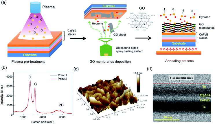
Experiments were carried out on sputter-deposited films with a layered structure of substrate/Ta(6)/Co40Fe40B20(t = 0.8–1.6)/MgAl–O(2)/Ta(3); the numbers in parentheses represent the thickness of the unit in nanometers. An MgAl–O layer was formed by RF sputtering from a sintered stoichiometric MgAl2O4 target. The films were annealed at 300 °C in a vacuum with a perpendicular magnetic field of about 8000 Oe for 1 hour. In order to improve the wettability of the films, the films were processed with oxygen plasma (Branson/IPC 3000 Plasma Asher, USA) for 20 min before depositing the GO membranes. The GO membranes were prepared by an ultrasonic-aided spray-casting system using commercial GO aqueous dispersions, presented in Fig. 1a.22,23 During the deposition process, the temperature of the films was kept at 25 °C, to maintain a proper evaporation rate of water molecules. The deposition process was repeated five times, with each single deposition lasting 8 s. The Raman spectra from two points on the films were obtained (Fig. 1b). The characteristic peaks, D, G, and 2D, are shown in the curves, their similarity clearly indicating the uniformity of the GO membranes.24,25 Since the roughness of the GO membranes has a significant influence on the performance of electronic devices, the surface morphology and a cross-sectional HRTEM image of the membrane-coated samples are shown in Fig. 1c and d, respectively, to demonstrate the good quality and relatively sharp interface of the GO membranes.Results and discussion
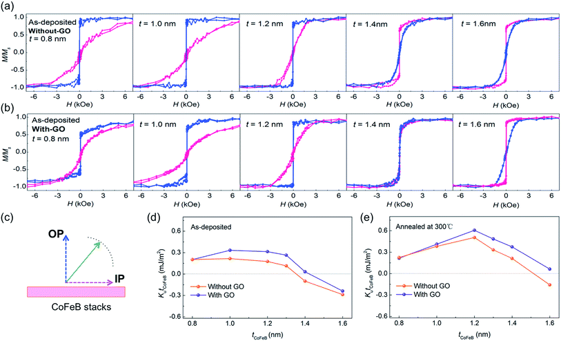
Fig. 2 shows the in-plane and out-of-plane magnetization (M–H) curves of the samples with and without the coating of GO membranes. The thickness of the CoFeB layers varies from 0.8 nm to 1.6 nm. The blue and red lines represent the out-of-plane (OP) and in-plane (IP) hysteresis curves with the magnetic field applied perpendicular or parallel to the plane of the samples, respectively. For the as-deposited film (not annealed), the OP direction was the easily magnetized axis in samples both with and without the GO membrane coating when tCoFeB = 0.8 nm, showing a well-squared shape. In the as-deposited samples without the GO membrane coating, the IP direction was the easily magnetized axis when tCoFeB = 1.4 nm (Fig. 2a); therefore, the turning point from OP to IP being the easily magnetized axis was tCoFeB = 1.3 nm. On the other hand, the turning point from OP to IP being the easily magnetized axis was tCoFeB = 1.4 nm in as-deposited samples with the GO membrane coating, as shown in Fig. 2b; the critical thickness for switching from the OP to the IP easy axis was extended by the GO membrane coating. Although the easy axis was IP when tCoFeB = 1.6 nm in the as-deposited samples both with and without the coating of GO membranes, the perpendicular saturation field decreased from 3000 Oe to 2000 Oe with the coating, indicating an enhanced contribution of PMA in the magnetization process. The enhancement of PMA of the as-deposited samples with GO coating is attributed to the fact that during the fabrication of CoFeB layer with the coating of GO membranes, the samples were put onto the hot plate at the temperature of 65 °C to dry the water of the GO dispersions. This heating effect could improve the interface between CoFeB and MgAlO barrier a little bit, and then enhance hybridization of Co(Fe) 3d and O 2p orbitals. After annealing (see ESI†), the PMA was enhanced for samples with tCoFeB from 1.0 to 1.4 nm, both with and without the GO membrane coating. The easy axis became OP with tCoFeB = 1.4 nm in the annealed sample without the GO membrane, while it became OP with tCoFeB = 1.6 nm in the annealed sample with the GO coating. Also, the in-plane saturation field increased from 2000 Oe to 4000 Oe in the coated samples with tCoFeB = 1.4 nm. These results indicate that the coating of GO membranes can significantly improve the PMA of CoFeB thin film.Generally, the effective magnetic anisotropy is composed of the contributions of the bulk anisotropy, the shape anisotropy, and the interfacial anisotropy.26 The effective anisotropy energy density (Ku) can be determined by taking the difference between the areas above the magnetization curves, measured along the hard and easy magnetic axes. Mathematically, Ku can be given by14
| Ku = Kb − 2πMs2 + Ki/tCoFeB |
After annealing, the PMA of the samples both with and without GO membranes is strongly enhanced, except when tCoFeB = 0.8 nm (Fig. 2e); a giant PMA of 0.6 mJ m−2 is achieved for a 1.2 nm thick CoFeB layer with GO membranes. First-principle calculations have shown that the PMA in a CoFeB–MgO system is mainly influenced by the hybridization of either Co 3d and O 2p orbitals, or Fe 3d and O 2p orbitals.14,27 Considering the changes in the hybridization of Co or Fe 3d and O 2p orbitals under the annealing temperature (300 °C), the enhanced PMA was probably caused by the increase in oxygen content at the interface between CoFeB and MgAl–O, and the improved crystalline structure of CoFeB and MgAl–O. However, the diffusion of C atoms from the functional groups of the GO membranes partially hindered the crystallinity of the CoFeB film. For the samples with tCoFeB = 0.8 nm, the PMA degradation probably originates from the inter-diffusion between Ta and CoFeB at the interface, and from the increased thickness of the magnetic dead layer.28
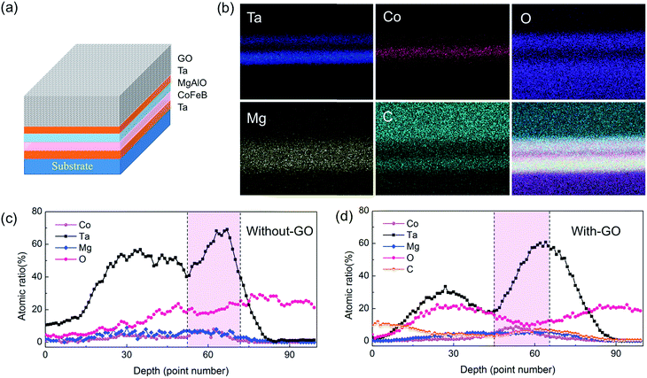
To further study the contribution of C atoms on the PMA, the high-angle annular dark-filed (HAADF) with line scan energy dispersive spectrum (EDS) was used to characterize the elemental distribution and stoichiometry of the samples both with and without GO membranes. Fig. 3b shows the constituting elements from the chemical distribution maps, from which the line-averaged profiles of the chemical element maps were generated (Fig. 3c). The EDS images clearly reveal that the C atoms diffused from the GO membranes to the interface between CoFeB and MgAl–O, even spreading into the CoFeB layer, unlike the CoFeB stacks without GO membranes. Here, we ascribe the PMA enhancement of the CoFeB layer with the coating of GO membranes to the hybridization of the C and Co(Fe) atoms, which is consistent with recent studies of PMA enhancement in graphene-coated and C60-covered Co surfaces.29–31
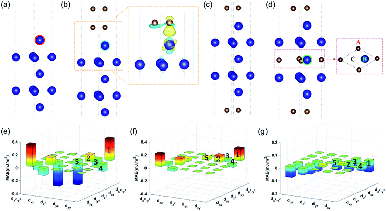
Generally, the PMA of CoFeB/MgAlO or MgO structures arises from the hybridization between Co(Fe) 3d and O 2p orbitals,32,33 as also demonstrated by the PMA of CoFeB without GO coating in this work. In addition, the binding energy of C 1s in C–O and C–C functional groups are 284.8 eV and 286.3 eV, respectively, indicating that C exceptional functional groups diffuse much easily. As shown in EDS images, the C atoms diffused from the GO membranes to the interface between CoFeB and MgAl–O, even spreading into the CoFeB layer, unlike the CoFeB stacks without GO membranes. Based on above considerations, we think the carbon atoms play important role in the enhancement of PMA of CoFeB with GO coating, in contrast with pure CoFeB/MgAlO heterostructures. Therefore, we performed first-principle calculations using the Vienna ab initio Simulation Package (VASP)34–37 to better understand the enhancement of the CoFeB PMA by the GO membrane coating, especially the influences of carbon atoms with different distribution relative to Co. We modeled a Co/layered-carbon system, because it has a simple atomic structure and the relevant mechanisms are believed to be similar to those of CoFeB/MgAl–O. In our calculations, the Co film was 5 monolayers (ML), or 10 Å. The in-plane lattice constant of the Co surface was fixed to the calculated bulk value of 2.5 Å. Five atomic layers of Co were included in the periodic supercell with 10 angstroms of vacuum to mitigate the interaction with the imaged Co layers. The electron–electron exchange–correlation was presented by generalized gradient approximation (GGA)34 following Perdew–Burke–Ernzerhof (PBE).35 The cutoff energy was set to 500 eV, with a 23 × 23 × 1 Monkhorst–Pack k-point mesh.37 Taking the spin–orbit coupling (SOC) effect into account, the energetically favorable direction, i.e., the easy axis of spontaneous magnetization, was determined by calculating the magnetic anisotropy energy (MAE):38
We first studied the MAE of the bare Co (001) surface, as shown in Fig. 4a. Fig. 4e shows the corresponding MAE contributions from the surface Co atom (circled). The dominant MAE contribution was positive and originated from the hybridization of the dxy and dx2−y2 orbitals (labeled 1). The total MAE was calculated to be 0.62 mJ m−2. Fig. 4b shows the atomic structure of the Co layer/double C atomic layers. The calculated MAE increased to 1.333 mJ m−2. The MAE contributions from the interfacial Co atom (circled) are shown in Fig. 4f. Although the hybridizations of the dxy and dx2−y2 orbitals (labeled 1 in Fig. 4e and f) and the dyz and dxz orbitals contributed less to the MAE, the contribution from the hybridization of the dyz and dz2 orbitals (labeled 5 in Fig. 4e and f) changed from negative to positive after introducing the C atoms, enhancing the overall MAE.
Experimentally, we found that the annealing process resulted in the partial diffusion of C through the CoFeB thin film, forming an additional counter interface. To take this additional interface into account, we built a structure of mono C atomic layer/Co layer/mono C atomic layer, as shown in Fig. 4c. The MAE further increased to 1.93 mJ m−2, almost 1.5 times that of the Co/double C atomic layer structure. However, we did not experimentally observe a substantial MAE enhancement after annealing. To address the discrepancy between the experiment and the theoretical calculations, we assumed that a certain amount of C atoms remained in the Co, contributing to the MAE in a different way. We studied an interstitial site C in the center of a Co slab. We also compared several highly symmetric C interstitial sites in the central Co layer (labeled A, B, and C) and found that the interstitial site A was the most stable, as shown in Fig. 4d. The calculated MAE was 1.508 mJ m−2, 1.5 times that of the Co/double C atomic layer structure. We analyzed the corresponding MAE contributions (Fig. 4g) from the Co atom in the layer next to the interface (circled). The MAE contribution changed from positive to negative during the hybridization of dxy and dx2−y2 (labeled 1). The contributions to MAE from the interfacial Co in this case were almost identical to those from the interfacial Co atom in the case of the Co/double C atomic layer structure. Therefore, due to the adverse effect of the interstitial site C on MAE, the overall MAE enhancement was suppressed.
Conclusion
In summary, we investigated the magnetic characteristics of CoFeB stacks, with and without a coating of GO membranes, both theoretically and experimentally. All of the results confirm that the GO membranes dramatically enhanced the PMA of a CoFeB/MgAl–O system. Our experiments found that the critical thickness for switching from an out-of-plane to an in-plane easy axis exceeds 1.6 nm after coating the CoFeB stacks with GO membranes, resulting in a giant PMA of 0.6 mJ m−2 when tCoFeB = 1.2 nm. The PMA of Co with the C atomic layer in a different location was studied through first-principles calculations. The PMA of the Co layers was mainly dominated by the interfacial 3d orbitals hybridization, even with an interstitial C defect. This comprehensive understanding of the PMA provides an alternative route for expanding the applications of GO membranes in graphene spintronics and for developing multifunctional graphene-composite spintronic devices.Experimental section
Samples with GO membranes fabrication
A medical ultrasonic atomization nebulizer (Omron Ultrasonic Nebulizer NB-150U, Japan) was used to prepare the fine mist of GO dispersion. To improve the wettability of the surface, the samples were processed by oxygen plasma (Branson/IPC 3000 Plasma Asher, USA) for 20 min before depositing the GO membranes. During the deposition process, temperature of the samples was set to be 25 °C for keeping a proper evaporation rate of water. The deposition process was repeated 5 times, with each single deposition lasting 8 s.Raman spectroscopy
The Raman spectra were acquired using a Horiba Evolution system.Magnetic measurement
The magnetic characteristics of the samples both with and without GO membranes were measured with vibrating sample magnetometer (Micro-sense EZ-VSM).Energy-dispersive X-ray spectroscopy
The elemental mapping shown in Fig. 3 was acquired using a built-in EDX measurement module in the STEM module of HITACHI S-4800 system. The probe size used in this case is 0.8 Å by FEI-Titan-G2 with Cs-corrected probe and it can distinguish 1 nm efficiently.Conflicts of interest
There are no conflicts to declare.Acknowledgements
This work was supported by National Natural Science Foundation (51501098, 61574083, 61434001), National Key R&D Program (2016YFA0200400), National Basic Research Program (2015CB352101), Special Fund for Agroscientific Research in the Public Interest (201303107) of China, Research Fund from Beijing Innovation Center for Future Chip, and Beijing Natural Science Foundation (No. 4164087). The authors are also thankful for the support of the Independent Research Program (2014Z01006) of Tsinghua University, in part by funding from King Abdullah University of Science and Technology (KAUST). J. F. acknowledges Youth Innovation Promotion Association of Chinese Academy of Sciences (No. 2017010). We would like to thank Dr Caihua Wan for discussions.Notes and references
- S. Das, R. Gulotty, A. V. Sumant and A. Roelofs, Nano Lett., 2004, 14, 2861 CrossRef PubMed.
- W. Han, R. K. Kawakami, M. Gmitra and J. Fabian, Nat. Nanotechnol., 2004, 9, 794 CrossRef PubMed.
- S. Z. Butler, et al., ACS Nano, 2013, 7, 2898 CrossRef CAS PubMed.
- B. Radisavljevic, A. Radenovic, J. Brivio, V. Giacometti and A. Kis, Nat. Nanotechnol., 2011, 6, 147 CrossRef CAS PubMed.
- L. Li, Y. Yu, G. Ye, Q. Ge, X. Ou, H. Wu, D. Feng, X. Chen and Y. Zhang, Nat. Nanotechnol., 2014, 9, 372 CrossRef CAS PubMed.
- D. Li and R. B. Kaner, Science, 2008, 320, 1170 CrossRef CAS PubMed.
- J. B. Oostinga, H. B. Heersche, X. Liu, A. F. Morpurgo and L. M. Vandersypen, Nat. Mater., 2007, 7, 151 CrossRef PubMed.
- N. Tombros, C. Jozsa, M. Popinciuc, H. T. Jonkman and B. J. V. Wees, Nature, 2007, 448, 571 CrossRef CAS PubMed.
- P. Avouris and C. Dimitrakopoulos, Mater. Today, 2012, 15, 86 CrossRef CAS.
- T. Y. Yang, J. Balakrishnan, F. Volmer, A. Avsar, M. Jaiswal, J. Samm, S. R. Ali, A. Pachoud and M. Zeng, Phys. Rev. Lett., 2011, 107, 1842 Search PubMed.
- T. Maassen, J. J. V. D. Berg, N. Ijbema, F. Fromm, T. Seyller, R. Yakimova and B. J. V. Wees, Nano Lett., 2012, 12, 1498 CrossRef CAS PubMed.
- B. S. Yang, J. Zhang, L. N. Jiang, W. Z. Chen, P. Tang, X.-G. Zhang, Y. Yan and X. F. Han, Phys. Rev. B, 2017, 95, 174424 CrossRef.
- S. Mangin, D. Ravelosona, J. A. Katine, M. J. Carey, B. D. Terris and E. E. Fullerton, Nat. Mater., 2006, 5, 210–215 CrossRef CAS.
- A. V. Khvalkovskiy, D. Apalkov, S. Watts, R. Chepulskii, R. S. Beach, A. Ong, X. Tang, A. Driskill-Smith, W. H. Butler, P. B. Visscher, D. Lottis, E. Chen, V. Nikitin and M. Krounbi, J. Phys. D: Appl. Phys., 2013, 46, 074001 CrossRef.
- S. Ikeda, K. Miura, H. Yamamoto, K. Mizunuma, H. D. Gan, M. Endo, S. Kanai, J. Hayakawa, F. Matsukura and H. Ohno, Nat. Mater., 2010, 9, 721 CrossRef CAS PubMed.
- W.-G. Wang, M. Li, S. Hageman and C. L. Chien, Nat. Mater., 2012, 11, 64 CrossRef CAS PubMed.
- H. Yang, A. D. Vu, A. Hallal, N. Rougemaille, J. Coraux, G. Chen, A. K. Schmid and M. Chshiev, Nano Lett., 2016, 16, 145 CrossRef CAS PubMed.
- A. D. Vu, J. Coraux, G. Chen, A. T. N'Diaye, A. K. Schmid and N. Rougemaille, Sci. Rep., 2016, 6, 24783 CrossRef CAS PubMed.
- R. R. Nair, H. A. Wu, P. N. Jayaram, I. V. Grigorieva and A. K. Geim, Science, 2012, 335, 442 CrossRef CAS PubMed.
- G. P. Liu, W. Q. Jin and N. P. Xu, Chem. Soc. Rev., 2015, 44, 5016 RSC.
- R. K. Joshi, P. Carbone, F. C. Wang, V. G. Kravets, Y. Su, I. V. Grigorieva, H. A. Wu, A. K. Geim and R. R. Nair, Science, 2014, 343, 752 CrossRef CAS PubMed.
- R. L. Peskin and R. J. Raco, J. Acoust. Soc. Am., 1963, 35, 1378 CrossRef.
- W. T. Mi, H. Y. Qi, H. M. Zhao, Y. X. Li, Y. Yang and T.-L. Ren, IEEE International Nanoelectronics Conference, 2016 Search PubMed.
- K. N. Kudin, B. Ozbas, H. C. Schniepp, R. K. Prud'Homme, I. A. Aksay and R. Car, Nano Lett., 2012, 8, 36 CrossRef PubMed.
- A. C. de Leon, L. Alonso, J. D. Mangadlao, R. C. Advincula and E. Pentzer, ACS Appl. Mater. Interfaces, 2017, 9, 14265 CAS.
- M. T. Johnson, P. J. H. Bloemen, F. J. A. D. Broeder and J. J. D. Vries, Rep. Prog. Phys., 1996, 59, 1409 CrossRef CAS.
- H. X. Yang, M. Chshiev, B. Dieny, J. H. Lee, A. Manchon and K. H. Shin, Phys. Rev. B: Condens. Matter Mater. Phys., 2011, 84, 054401 CrossRef.
- B. Tao, D. Li, Z. Yuan, H. Liu, S. Ali, J. Feng, H. Wei, X. Han, Y. Liu and Y. Zhao, Appl. Phys. Lett., 2014, 105, 36 Search PubMed.
- K. Bairagi, A. Bellec, V. Repain, C. Chacon, Y. Girard, Y. Garreau, J. Lagoute, S. Rousset, R. Breitwieser and Y. C. Hu, Phys. Rev. Lett., 2015, 114, 247203 CrossRef CAS PubMed.
- R. Decker, J. Brede, N. Atodiresei, V. Caciuc, S. Blügel and R. Wiesendanger, Phys. Rev. B: Condens. Matter Mater. Phys., 2013, 87, 041403 CrossRef.
- V. M. Karpan, G. Giovannetti, P. A. Khomyakov, M. Talanana, A. A. Starikov, M. Zwierzycki, J. VandenBrink, G. Brocks and P. J. Kelly, Phys. Rev. Lett., 2007, 99, 176602 CrossRef CAS PubMed.
- G. Y. Shi, C. H. Wan, Y. S. Chang, F. Li, X. J. Zhou, P. X. Zhang, J. W. Cai, X. F. Han, F. Pan and C. Song, Phys. Rev. B, 2017, 95, 104435 CrossRef.
- C. Song, B. Cui, F. Li, X. J. Zhou and F. Pan, Prog. Mater. Sci., 2017, 87, 33 CrossRef.
- J. P. Perdew, J. A. Chevary, S. H. Vosko, K. A. Jackson, M. R. Pederson, D. J. Singh and C. Fiolhais, Phys. Rev. B: Condens. Matter Mater. Phys., 1992, 46, 6671 CrossRef CAS.
- J. P. Perdew, K. Burke and M. Ernzerhof, Phys. Rev. Lett., 1996, 77, 3865–3868 CrossRef CAS PubMed.
- D.-S. Wang, R. Q. Wu and A. J. Freeman, Phys. Rev. B: Condens. Matter Mater. Phys., 1993, 47, 14932 CrossRef CAS.
- G. Kresse, J. Furthmuller and W. Universität, VASP-Guide, 2014 Search PubMed.
- V. B. Shenoy, Phys. Rev. B: Condens. Matter Mater. Phys., 2005, 71, 094104 CrossRef.
Footnote |
| † Electronic supplementary information (ESI) available. See DOI: 10.1039/c7ra08644j |
| This journal is © The Royal Society of Chemistry 2017 |


