
 Open Access Article
 This Open Access Article is licensed under a
 Creative Commons Attribution 3.0 Unported Licence
Growth, characterization, and thin film transistor application of CH3NH3PbI3 perovskite on polymeric gate dielectric layers†
Jenner H. L. Ngai‡
ab,
Johnny K. W. Ho‡ a,
Rocky K. H. Chana,
S. H. Cheunga,
Louis M. Leungb and
S. K. So*a
a,
Rocky K. H. Chana,
S. H. Cheunga,
Louis M. Leungb and
S. K. So*a
aDepartment of Physics and Institute for Advanced Materials, Hong Kong Baptist University, Kowloon Tong, Hong Kong, China. E-mail: skso@hkbu.edu.hk
bDepartment of Chemistry, Hong Kong Baptist University, Kowloon Tong, Hong Kong, China
First published on 23rd October 2017
Abstract
Methylammonium-based perovskite compounds are generally grown on conducting or semiconducting substrates for high performance solar cell applications. In this study, we explore the growth of these compounds on insulators and test for their field-effect transistor performance. The key challenge is to find a surface that favors the crystal growth of perovskites without compromising the adhesion of the crystals. A family of methacrylate-based polymers has been identified as the insulators. Onto these insulators, methylammonium lead iodide polycrystalline thin films were grown. Generally, we found that the crystal size in the perovskite layers is well-correlated with the surface hydrophobicity. More hydrophobic polymer layers favor the growth of larger crystals, but result in less favorable adhesion of the perovskite. Methacrylate polymers with a phenyl substituent can give better adhesion and crystal sizes despite their hydrophobic properties. Among the different insulating polymer layers, we found that poly(phenyl methacrylate) (PPhMA), a derivative of the common commercial plastic poly(methyl methacrylate) (PMMA), produces the best perovskite films. The molecular origin of these properties is discussed. To test the electronic properties of these films, we employed them for thin-film transistor applications. Under optimal conditions, the thin-film transistors fabricated on PPhMA produce the best device with an electron mobility of 0.4 cm2 V−1 s−1. Our results are also supported by photothermal deflection spectroscopy investigations of the subgap optical absorptions of these films.
1 Introduction
Solution processable organic–inorganic hybrid perovskite films have become probably the most hotly contended material in photovoltaics (PV) within a short span of a few years.1–3 Power conversion efficiencies (PCEs) of perovskite-based solar cells have surged from 3.8 to 22.1% and more.4 As high quality polycrystalline thin films of perovskites are essential for PV devices with stable and high PCEs,5 numerous studies have already been devoted to the study of the growth of perovskite films on conducting or semiconducting surfaces.6Besides PV applications, perovskites should be identified as a multi-functional electronic material.7–10 Several properties make the multi-functionality appealing. These include sharp optical bandedge,7 small exciton binding energy,8 long carrier lifetime,9 and high charge carrier mobility10 to name a few. These outstanding optoelectronic properties should position perovskite compounds for use in a wide range of devices beyond solar cells. Conceivable examples are photodetectors, lasers, light-emitting diodes, and thin-film transistors (TFTs). The key advantages of perovskite TFTs are their potential to achieve high mobility and processability. Most high performance OTFT materials have semi-crystalline structures or favorable intermolecular packing which enables effective charge hopping,11 and these require carefully designed molecular structures and specific processing conditions.12,13 Compared to pure OTFTs, it is relatively easier to obtain high crystallinity perovskite-based transistor materials. A hole mobility of >100 cm2 V−1 s−1 and electron mobility of >20 cm2 V−1 s−1 have been revealed in methylammonium lead iodide perovskite single crystals,9 and the intrinsic mobility limited by the acoustic phonon scattering can go up to a few thousand cm2 V−1 s−1.14 Perovskite materials can also be solution processed, which is particularly suitable for printed electronics.15
Despite the appealing potential breakthrough offered by perovskite materials, the applications in TFT are still quite limited.16–20 One of the key hurdles for the fabrication of TFTs is the identification of a suitable dielectric layer for the growth of perovskite crystals.21,22 This hurdle is especially challenging for solution processable perovskite films for TFTs. Broadly speaking, gate dielectric layers can either be hydrophilic or hydrophobic. For a hydrophilic gate dielectric layer, perovskites are known to adhere favorably.23 However, the strong interactions between the gate layer and perovskite prevent the growth of large crystals at the interface. The presence of small crystallite hinders charge carrier transport along the conducting channel, and results in poor TFT performance. For a hydrophobic dielectric, the wetting of the perovskite from a solution precursor is poor, and thus forbids the growth of any continuous films, which is essential for TFTs. Thus, a compromise must be made in terms of the hydrophobicity of the underlying gate dielectric layer.
In this contribution, we identified several polymeric methacrylate (MA)-based polymers, and characterized their thin film hydrophobicities. We then grew methylammonium lead iodide (CH3NH3PbI3) perovskite films on these polymers using solution processing techniques. The methacrylate polymers chosen were poly(methyl methacrylate) (PMMA), poly(ethyl methacrylate) (PEMA), poly(isopropyl methacrylate) (PiPMA), poly(isobutyl methacrylate) (PiBMA) and poly(phenyl methacrylate) (PPhMA). They possess sound thermal and chemical stability, and are available commercially. The series of methacrylate polymers also provides a systematic way to study how surface hydrophobicity affects the growth of perovskites. Besides these five polymers, polystyrene (PS) was also examined as a control in order to demonstrate the role of the methacrylate functional group in the growth of the perovskite films. The chemical structures of all these polymers are shown in Fig. 1. We found a clear correlation between the hydrophobicity and the size and qualities of the perovskite crystals. Furthermore, we demonstrate how to use these perovskite films to fabricate bottom-gate top-contact TFTs having a highest mobility of about 0.40 cm2 V−1 s−1.
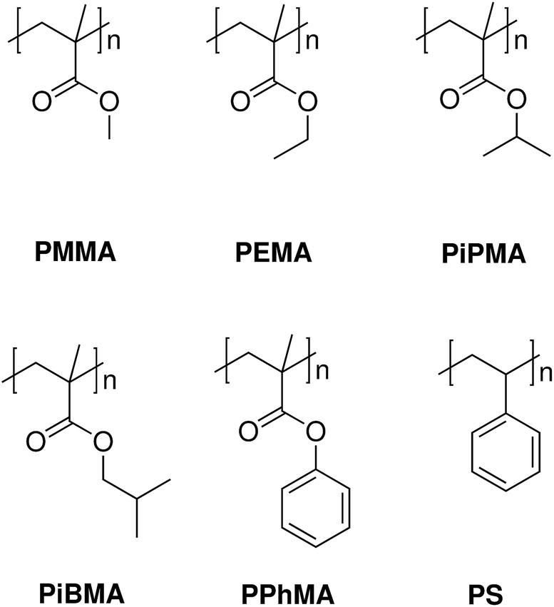 | ||
| Fig. 1 The polymers used to study the growth of the perovskite on different hydrophobic surfaces. | ||
2 Experimental
Lead(II) iodide 99% (PbI2), poly(methyl methacrylate) (PMMA), poly(ethyl methacrylate) (PEMA), poly(isobutyl methacrylate) (PiBMA), poly(phenyl methacrylate) (PPhMA), and polystyrene (PS) were purchased from Sigma Aldrich. Poly(isopropyl methacrylate) (PiPMA) was purchased from Polysciences, Inc. Methylammonium iodide (MAI) was purchased from Tokyo Chemical Industry Co., Ltd (TCI). PbI2 was dissolved in dimethylformamide (DMF) in a concentration of 450 mg mL−1 and stirred at 70 °C overnight. MAI was dissolved in isopropanol at a concentration of 45 mg mL−1 and stirred at 70 °C overnight. All perovskite films were grown on heavily p-doped silicon substrates which were thermally grown with 300 nm of SiO2. The substrates were washed by sonication in deionized water, acetone, methanol and isopropanol followed by ultraviolet-ozone treatment. Afterwards, polymer solutions in chlorobenzene were spin-coated onto the substrates and dried at 100 °C for 1 hour in a nitrogen-filled glovebox. The dried polymer films served as the substrate layer for the growth of the perovskite films. We employed a 2-step approach to grow the perovskite films. Firstly, PbI2 dissolved in DMF was spin-coated on top of the polymer layer at 1200 rpm for 60 s and was subsequently annealed at 70 °C for 1 hour. Solvent annealing was carried out using the same conditions with 10 μL of DMF droplets next to the samples, and covered with a glass Petri dish during the solvent annealing. Secondly, the MAI solution in isopropanol was then deposited onto the PbI2 layer at 1200 rpm for 60 s. Finally, thermal and solvent annealing were performed on the samples using a similar procedure described above except the temperature for annealing was 100 °C.The hydrophobicity of the polymer films was investigated by contact angle measurements. The measurements were carried out using a digital camera to capture an image of a 5.0 μL water droplet on the thin-film polymer. The contact angle is the angle between the tangent of the water droplet and the wafer surface. The morphologies of the perovskite films were investigated using scanning electron microscopy (SEM) (LEO Gemini 1530). The average crystal size of the perovskite crystals on different polymers was calculated automatically by the software ImageJ using the SEM images of the perovskite crystal grains captured at 10000× magnification. The crystallinity of the films was evaluated using grazing incidence X-ray diffraction (GIXRD) with a Bruker AXS D8 Advance X-ray Diffractometer. The perovskite films with satisfactory crystal qualities were further used for thin-film transistor (TFT) fabrication. A bottom-gate top-contact architecture was employed for the TFTs. Gold (100 nm) source (S) and drain (D) electrodes were deposited via thermal evaporation through a shadow mask, defining a channel length (L) of 50 μm and a channel width (W) of 6 mm. The electrical performance measurements of the TFT devices were carried out in a cryostat (Oxford Instruments, Optistat DN-V) under high vacuum (10−5 Torr) and dark conditions at various temperatures and measured by a Keithley 236 source measurement unit together with a Xantrex XT 120-0.5 as the DC gate voltage supply.
3 Results and discussion
3.1 Perovskite film growth on the polymeric insulators
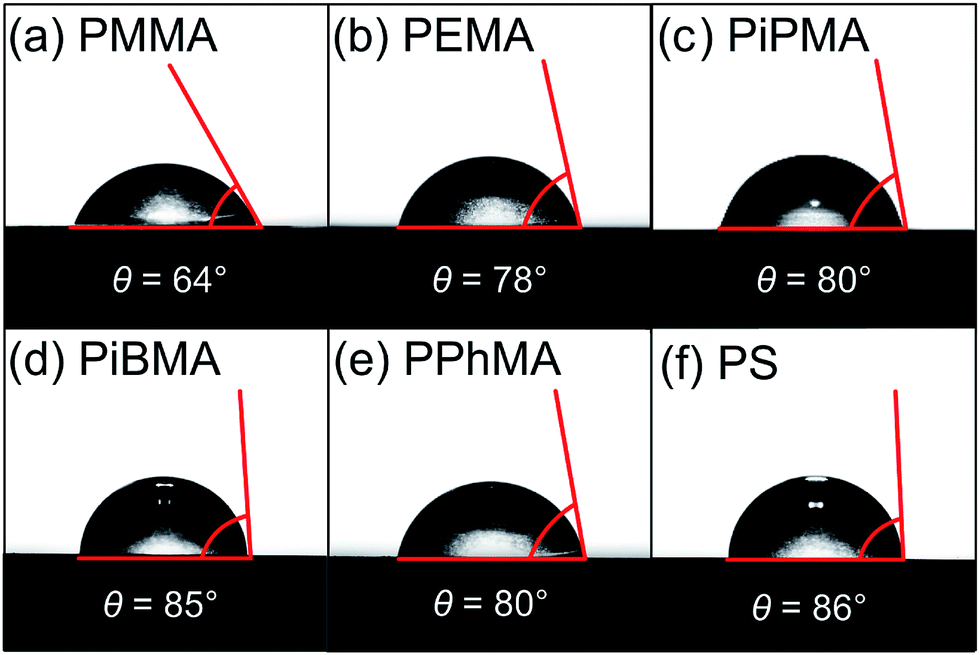 | ||
| Fig. 2 Contact angles of a water droplet on the polymer substrates: (a) PMMA; (b) PEMA; (c) PiPMA; (d) PiBMA; (e) PPhMA and (f) PS. | ||
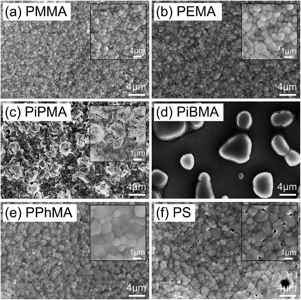 | ||
| Fig. 3 SEM images of the perovskite crystals on the polymer substrates: (a) PMMA; (b) PEMA; (c) PiPMA (poor wetting, non-uniform film); (d) PiBMA (non-wetting); (e) PPhMA and (f) PS (poor adhesion with physical pinholes). | ||
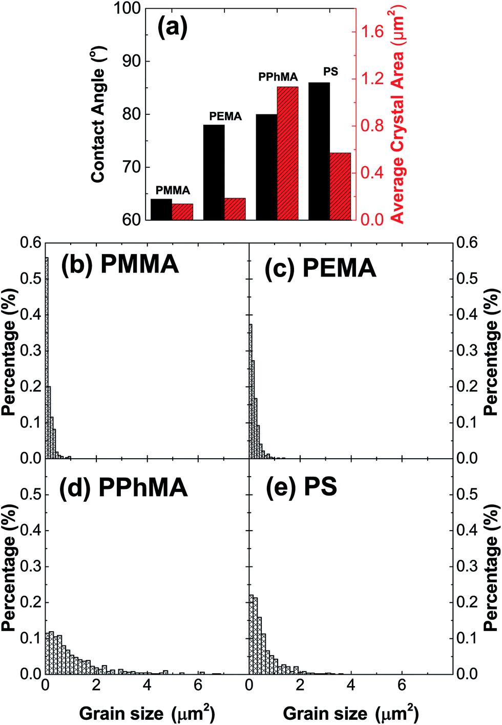 | ||
| Fig. 4 (a) Relationship between contact angle and average perovskite crystal size on different polymer substrates, with the corresponding distribution histograms of (b) PMMA, (c) PEMA, (d) PPhMA and (e) PS substrates. | ||
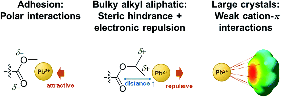
Below, we briefly discuss the molecular origin of crystal growth on the MA polymers based on the criterion of adhesion in relation to hydrophobicity and how it influences perovskite crystal growth. In the MA polymers, electronegative oxygen atoms and some side groups as substituents attached to the oxygen atoms can be found. An adhesion contribution by the hydrophilic O atoms can be revealed from a control experiment of the growth of perovskite crystals on PS in which O atoms are missing. Surprisingly, comparing PPhMA and PS, perovskite crystals with an average size of 0.57 μm2 can be observed on the PS surface with numerous pinholes, as revealed by the SEM image [Fig. 3(f)], indicating that the crystals might not adhere well on the hydrophobic PS surface. From this, we postulate that the O atoms in the MA group provide initial nucleation sites to the polymer and give better adhesion. A similar observation was reported recently by Grätzel et al. who suggested that the methacrylate moiety can act as a support and scaffold to induce nucleation of the perovskite crystal growth.1
The correlation between crystal size and the difference in hydrophobicity can be attributed to the substituent effect on the methacrylate polymer, in an order of methyl < ethyl < phenyl [Fig. 4(a)]. For PiPMA and PiBMA, which have isopropyl and isobutyl substituents respectively, PiPMA gives a poorly-wetting surface where perovskite crystals can hardly form on it, resulting in a poorly developed and non-uniform film [Fig. 3(c)], and PiBMA simply gives a non-wetting surface for the PbI2 solution [Fig. 3(d)]. On the PiPMA and PiBMA surfaces, the alkyl groups are so bulky that they may hinder the interactions between the O atoms on the MA polymer and the Pb2+ ions during the spin-coating process of PbI2. The longer the alkyl substituent, the greater the steric hindrance for the O atom nucleation sites. Moreover, the electropositive hydrogen atoms in the alkyl groups could appear repulsive to the Pb2+ ions. Thus, the electronic interactions between the O atoms and the Pb2+ ions would be weakened [Fig. 5]. In other words, the bulky alkyl groups act as a barrier to the adhesion of PbI2 on the surfaces for crystal nucleation at the early stage of PbI2 deposition, leading to poor crystal growth on such surfaces. When the substituents are small (e.g. methyl and ethyl), as shown in Fig. 5, the inductive effect from these electron donating groups can enhance the interaction between the O atoms and the Pb2+ ions, giving rise to larger crystal sizes. Here, it can be hypothesized that the side groups in the MA moieties can regulate the size and quality of the crystals during the crystal growth process with the SEM and crystal size statistical data [Fig. 3(a), (b) and 4(a)], and that the SEM results of the poorly developed films on PiPMA and the non-wetting surface on PiBMA support the role of the O atoms in the Pb2+ ion adhesion on the polymer surfaces by demonstrating the masking effect of the O atoms due to the bulky aliphatic isopropyl and isobutyl groups. It is also important to note that the correlation between the crystal size and surface hydrophobicity should only be valid in the same polymer series.
 | ||
| Fig. 5 Different interactions between the moieties in the polymers and the Pb2+ ion during the spin-coating process of PbI2 solution onto them. | ||
It is worth noting that, despite the similar hydrophobicity of PiPMA and PPhMA as observed via the contact angle measurements, PPhMA gave a well-wetted perovskite film but PiPMA gave a poorly-wetting surface for perovskite growth. Therefore, compared to aliphatic substituents (e.g. methyl and ethyl), aromatic substituents (e.g. phenyl) provided better benefits of obtaining large and high quality perovskite crystals as shown in the case of PPhMA [Fig. 4(e)]. The beneficial effect of PPhMA on perovskite growth may possibly be due to the additional weak cation–π interactions between the Pb2+ ions and the phenyl groups,24,25 as shown in Fig. 5. Such interaction may assist the perovskite growth during the annealing process, and thus provide extra support to the coordinational crystal growth besides the polar interaction between the O atom nucleation sites and the Pb2+ ions. Therefore, the presence of both the O atoms and the phenyl groups functioned synergistically to the crystal growth, resulting in the highest crystal quality and the greatest crystal size. On the other hand, the study of perovskite growth on the hydrophobic PS surface demonstrated the effect of the sole cation–π interactions between the phenyl groups and Pb2+ ions without any O atoms as nucleation sites. The perovskite crystals on PS could still be grown owing to the cation–π interactions which helped nucleation. However, the cation–π interaction is much weaker than the interaction between polar electronegative atoms and the Pb2+ ions once the perovskite crystal growth was completed. Thus, without the electronegative oxygen atoms in PS, crystal adhesion is significantly weakened and numerous pinholes evenly distributed on the PS surface were found. As for PiPMA and PiBMA, with both the absence of the phenyl groups and the weakened polar interaction from the O atoms due to the bulky and electropositive aliphatic alkyl side groups, Pb2+ adhesion on these surfaces on which perovskite crystals can hardly form is found to be difficult.
In summary, our study found out the following in relation to obtaining large and quality CH3NH3PbI3 perovskite polycrystalline films on MA polymers: (1) electronegative O atoms are beneficial to perovskite nucleation events and adhesion of perovskite on the surface; (2) appropriate choices of aliphatic alkyl substituents in the MA group balancing the counteracting inductive effect and steric effect together with repulsively electronic interactions give well-adhered and regulated large perovskite crystal surfaces; and (3) aromatic (phenyl) substituents offer cation–π interactions and help develop large perovskite crystals.
3.2 Electronic properties of the perovskite films
Fig. 6 shows the subgap optical absorption of the perovskite films on the different polymers. For each absorption spectrum, a sharp drop in absorption occurs at above 1.6 eV, which matches very well with the known energy gap of CH3NH3PbI3.29 The “steepness” of the absorption just below the bandgap energy can be evaluated by the Urbach model:
 | (1) |
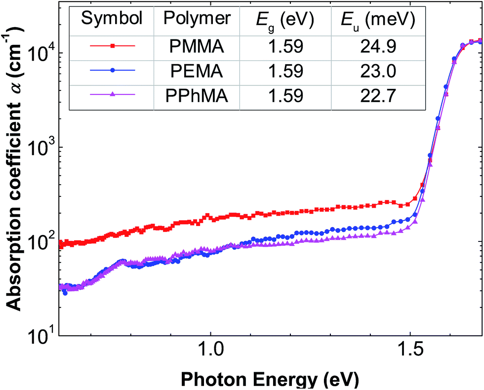 | ||
| Fig. 6 Photothermal deflection spectra of the perovskite on the different polymer gate dielectric surfaces. The corresponding values of bandgap Eg and Urbach energy Eu are shown in the inset table. | ||
 | (2) |
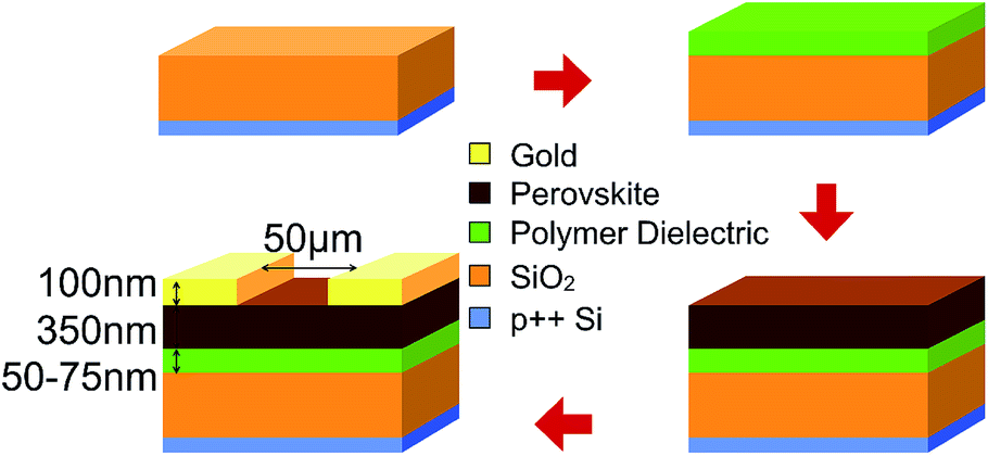 | ||
| Fig. 7 Schematic diagram showing the fabrication procedure of the bottom-gate-top-contact (BGTC) perovskite TFT devices. | ||
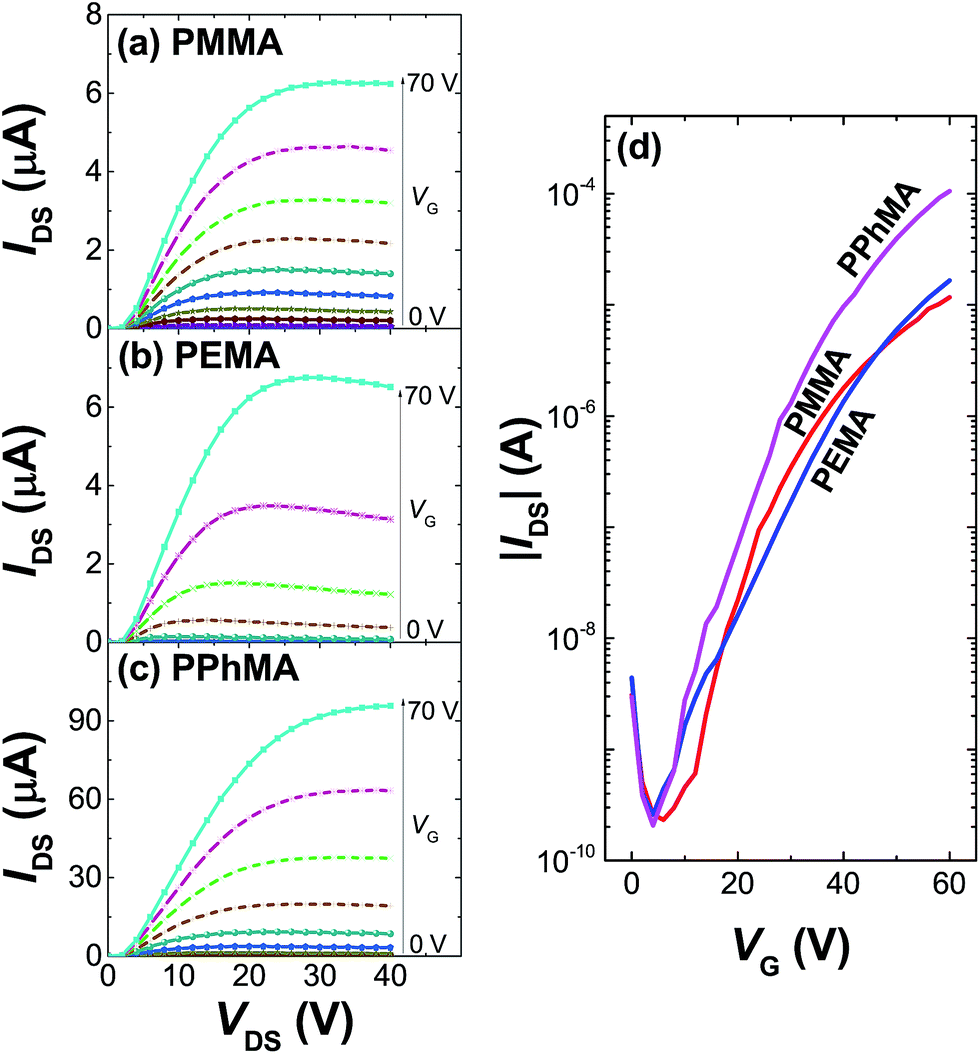 | ||
| Fig. 8 Output characteristics of the perovskite TFT at 202 K on the (a) PMMA, (b) PEMA and (c) PPhMA polymer substrates. (d) Transfer characteristics at VDS = 40 V of the perovskite TFT at 202 K on the three polymer gate dielectric surfaces. | ||
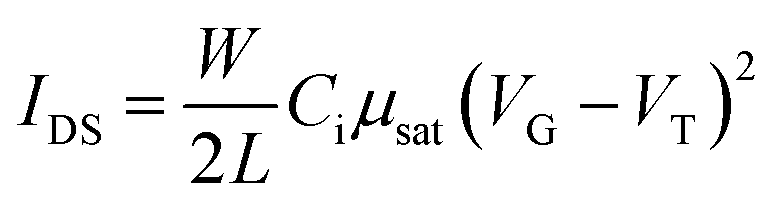
Table 1 summarizes the TFT data at 202 K. The electron mobility of the perovskite thin film improves from PEMA < PMMA < PPhMA. Again, the best device corresponds to the perovskite grown on PPhMA. The TFT mobilities for the perovskite on PMMA and PEMA are similar, of the same order of 0.03–0.05 cm2 V−1 s−1, possibly due to their similar crystal sizes, despite the slightly larger mobility of PMMA than its PEMA counterpart. For the PPhMA device, the substantially larger crystallites [Fig. 4(a)] implies fewer grain boundaries which enhance charge carrier transport.
| Dielectric | Ci (nF cm−2) | μsat (cm2 V−1 s−1) | VT (V) | Ion/off |
|---|---|---|---|---|
| PMMA | 9.06 | 0.056 | 31.6 | 5.0 × 10⁴ |
| PEMA | 8.89 | 0.030 | 45.7 | 1.3 × 10⁵ |
| PPhMA | 9.19 | 0.40 | 34.3 | 5.1 × 10⁵ |
The TFT device using PPhMA as the best gate dielectric material was also given an operational stability test. The device was kept at 202 K under high vacuum (10−5 Torr) for an extended period of time and the variation of the electron mobility was recorded as shown in Fig. 9. After an initial slight drop, the electron mobility retained little decrease even after 400 hours despite the electrical stress given during the repeated measurements. The half-life of the device is estimated as 300 hours. The operational stability of the device without engineering-level optimization was preliminarily found encouraging, and further work can be done on enhancing its tolerance under electrical stress.
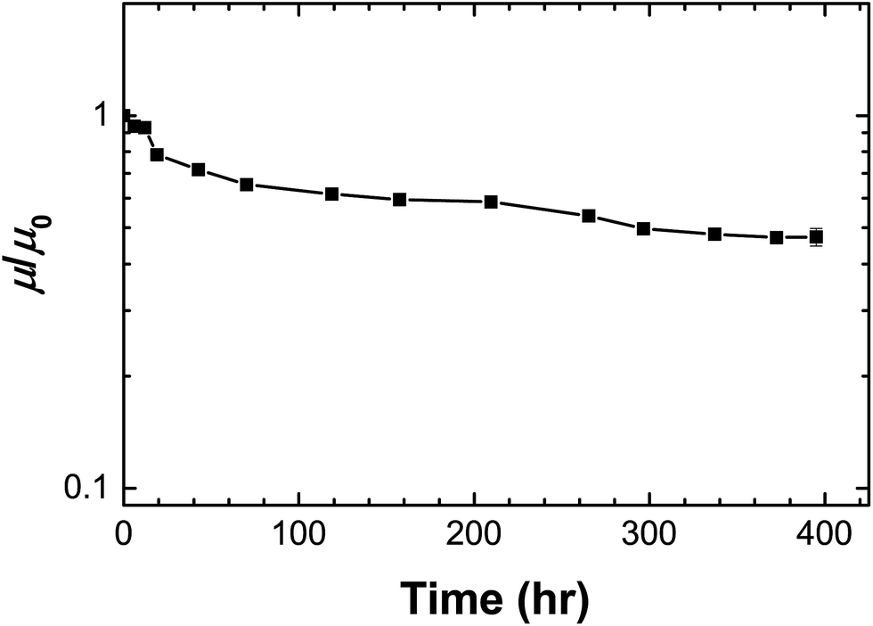 | ||
| Fig. 9 Operational stability of the TFT device at 202 K using PPhMA as the gate dielectric material. μ/μ0 is the normalized mobility. | ||
Finally, we want to briefly comment on how temperature influences charge transport in perovskite transistors. In the low temperature regime, as the temperature is reduced from 200 K towards 100 K, a gentle increase in the mobility was observed. The increase in mobility in this temperature range can be attributed to the reduction of lattice scattering or phonon vibrations of the crystals. However, as T increases to above 250 K, a significant reduction in mobility occurs for all samples. At room temperature, mobilities are reduced by at least 2 orders. The sharp reduction in mobility starting at 250 K can be attributed to the phase transition of the perovskite crystals from the orthorhombic phase to the tetragonal phase as depicted in Fig. 10.19 Furthermore, it was suggested that the electron mobility and unit cell structure are correlated.14,30,31 From Fig. 10, it can be seen that the cage size of the tetragonal phase is relatively large, and so the structure facilitates the motions of the iodide or methylammonium ions. These ions give rise to electronic disorder that can trap electrons or scatter electron motions. Thus, electron transport is severely affected by these relatively mobile ions in the tetragonal phase.
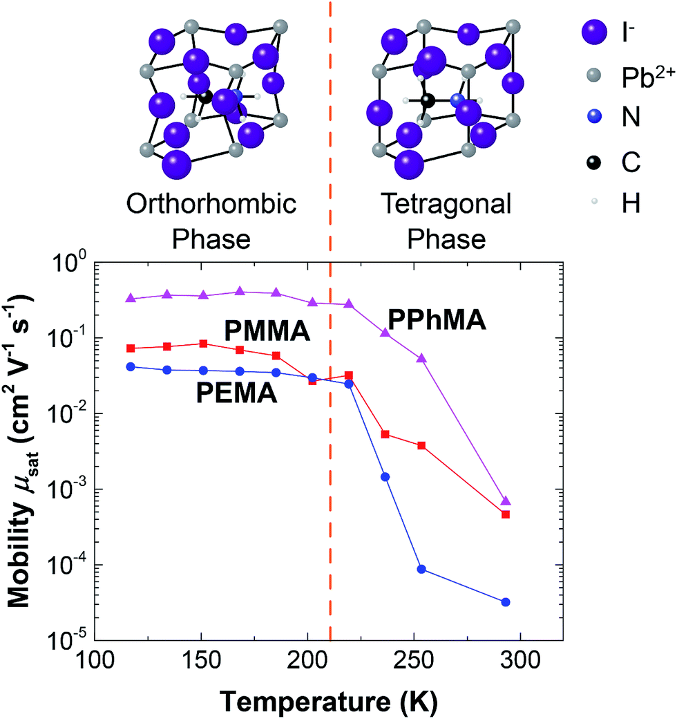 | ||
| Fig. 10 Electron mobility against temperature of the perovskite TFT using the different gate dielectric materials. The models on top indicate the different phases of CH3NH3PbI3 at different temperature regions. | ||
4 Conclusions
The growth and electronic qualities of methylammonium lead iodide polycrystalline film on several methyl methacrylate-based polymer insulators were investigated. We found that the film growth via solution processing is a competition between film adhesion and crystal size. The less hydrophobic methacrylate-based polymer favors film formation but results in films with small crystallites with an island area of about 0.2 μm2. More hydrophobic polymers potentially result in much larger but non-adhering crystals. Among the methacrylate-based polymers tested, PPhMA offers the best compromise. It possesses the necessary O atoms in the methacrylate groups for inducing the initial nucleation of the precursor PbI2, and at the same time, the presence of the phenyl ring provides cation–π interactions between the polymer surface and Pb2+ ions with good hydrophobicity to favor large crystal growth. Perovskite films grown on PPhMA surfaces result in the largest and tightly packed crystallites, with an average size of 1.1 μm2. Electronic evaluation of these films indicates a sharp bandgap at 1.6 eV and the smallest Urbach energy of 22.7 meV. Using perovskites on PPhMA as the active layer for TFTs, an impressive TFT mobility of 0.40 cm2 V−1 s−1 can be achieved. The findings here may allow future researchers to develop new polymer additives that can assist or promote perovskite crystal growth in specific morphologies for varied device applications.Conflicts of interest
There are no conflicts to declare.Acknowledgements
Support of this research by the research committee of HKBU and the Research Grant Council of Hong Kong under Grant #’s FRG2/14-15/092, HKBU211913 and HKBU12201914 is gratefully acknowledged.References
- D. Bi, C. Yi, J. Luo, J.-D. Décoppet, F. Zhang, S. M. Zakeeruddin, X. Li, A. Hagfeldt and M. Grätzel, Nat. Energy, 2016, 1, 16142 CrossRef CAS.
- Y. Zhao and K. Zhu, Chem. Soc. Rev., 2016, 45, 655–689 RSC.
- S. Yang, W. Fu, Z. Zhang, H. Chen and C.-Z. Li, J. Mater. Chem. A, 2017, 5, 11462–11482 CAS.
- J.-P. Correa-Baena, A. Abate, M. Saliba, W. Tress, T. J. Jacobsson, M. Grätzel and A. Hagfeldt, Energy Environ. Sci., 2017, 10, 710–727 CAS.
- A. Dualeh, N. Tétreault, T. Moehl, P. Gao, M. K. Nazeeruddin and M. Grätzel, Adv. Funct. Mater., 2014, 24, 3250–3258 CrossRef CAS.
- Y.-X. Chen, Q.-Q. Ge, Y. Shi, J. Liu, D.-J. Xue, J.-Y. Ma, J. Ding, H.-J. Yan, J.-S. Hu and L.-J. Wan, J. Am. Chem. Soc., 2016, 138, 16196–16199 CrossRef CAS PubMed.
- Y. Cheng, H.-W. Li, J. Qing, Q.-D. Yang, Z. Guan, C. Liu, S. H. Cheung, S. K. So, C.-S. Lee and S.-W. Tsang, J. Mater. Chem. A, 2016, 4, 12748–12755 CAS.
- Q. Lin, A. Armin, R. C. R. Nagiri, P. L. Burn and P. Meredith, Nat. Photonics, 2015, 9, 106–112 CrossRef CAS.
- Q. Dong, Y. Fang, Y. Shao, P. Mulligan, J. Qiu, L. Cao and J. Huang, Science, 2015, 347, 967–970 CrossRef CAS PubMed.
- Y. Liu, Z. Yang, D. Cui, X. Ren, J. Sun, X. Liu, J. Zhang, Q. Wei, H. Fan and F. Yu, et al., Adv. Mater., 2015, 27, 5176–5183 CrossRef CAS PubMed.
- H. Sirringhaus, Adv. Mater., 2014, 26, 1319–1335 CrossRef CAS PubMed.
- Z. Bao and J. Locklin, Organic field-effect transistors, CRC press, 2007 Search PubMed.
- C. Reese, M. Roberts, M. M. Ling and Z. Bao, Mater. Today, 2004, 7, 20–27 CrossRef CAS.
- T. Zhao, W. Shi, J. Xi, D. Wang and Z. Shuai, Sci. Rep., 2016, 6, 19968 CrossRef PubMed.
- A. Chilvery, S. Das, P. Guggilla, C. Brantley and A. Sunda-Meya, Sci. Technol. Adv. Mater., 2016, 17, 650–658 CrossRef PubMed.
- D. Li, G. Wang, H.-c. Cheng, C.-y. Chen, H. Wu, Y. Liu, Y. Huang and X. Duan, Nat. Commun., 2016, 7, 11330 CrossRef CAS PubMed.
- G. Wang, D. Li, H.-C. Cheng, Y. Li, C.-Y. Chen, A. Yin, Z. Zhao, Z. Lin, H. Wu and Q. He, et al., Sci. Adv., 2015, 1, e1500613 Search PubMed.
- F. Li, C. Ma, H. Wang, W. Hu, W. Yu, A. D. Sheikh and T. Wu, Nat. Commun., 2015, 6, 8238 CrossRef PubMed.
- X. Y. Chin, D. Cortecchia, J. Yin, A. Bruno and C. Soci, Nat. Commun., 2015, 6, 7383 CrossRef CAS PubMed.
- Y. Mei, C. Zhang, Z. V. Vardeny and O. Jurchescu, MRS Commun., 2015, 5, 297–301 CrossRef CAS.
- C. Bi, Q. Wang, Y. Shao, Y. Yuan, Z. Xiao and J. Huang, Nat. Commun., 2015, 6, 7747 CrossRef CAS PubMed.
- D. Zhao, M. Sexton, H.-Y. Park, G. Baure, J. C. Nino and F. So, Adv. Energy Mater., 2015, 5, 1401855 CrossRef.
- T. Salim, S. Sun, Y. Abe, A. Krishna, A. C. Grimsdale and Y. M. Lam, J. Mater. Chem. A, 2015, 3, 8943–8969 CAS.
- J. C. Ma and D. A. Dougherty, et al., Chem. Rev., 1997, 97, 1303–1324 CrossRef CAS PubMed.
- N. Zacharias and D. A. Dougherty, Trends Pharmacol. Sci., 2002, 23, 281–287 CrossRef CAS PubMed.
- W. B. Jackson, N. M. Amer, A. Boccara and D. Fournier, Appl. Opt., 1981, 20, 1333–1344 CrossRef CAS PubMed.
- A. Boccara, W. Jackson, N. M. Amer and D. Fournier, Opt. Lett., 1980, 5, 377–379 CrossRef CAS PubMed.
- C. H. Y. Ho, S. H. Cheung, H.-W. Li, K. L. Chiu, Y. Cheng, H. Yin, M. H. Chan, F. So, S.-W. Tsang and S. K. So, Adv. Energy Mater., 2017, 7, 1602360 CrossRef.
- G. E. Eperon, S. D. Stranks, C. Menelaou, M. B. Johnston, L. M. Herz and H. J. Snaith, Energy Environ. Sci., 2014, 7, 982–988 CAS.
- S. P. Senanayak, B. Yang, T. H. Thomas, N. Giesbrecht, W. Huang, E. Gann, B. Nair, K. Goedel, S. Guha and X. Moya, et al., Sci. Adv., 2017, 3, e1601935 CrossRef PubMed.
- P. S. Whitfield, N. Herron, W. E. Guise, K. Page, Y. Q. Cheng, I. Milas and M. K. Crawford, Sci. Rep., 2016, 6, 35685 CrossRef CAS PubMed.
Footnotes |
| † Electronic supplementary information (ESI) available. See DOI: 10.1039/c7ra08699g |
| ‡ These authors contributed equally to this work. |
| This journal is © The Royal Society of Chemistry 2017 |