 Open Access Article
Creative Commons Attribution 3.0 Unported Licence
Shining a light on transition metal chalcogenides for sustainable photovoltaics
Peter D.
Matthews
 a,
Paul D.
McNaughter
 a,
David J.
Lewis
 b and
Paul
O'Brien
 *ab
*ab
aSchool of Chemistry, University of Manchester, Oxford Road, Manchester, M13 9PL, UK. E-mail: paul.o'brien@manchester.ac.uk
bSchool of Materials, University of Manchester, Oxford Road, Manchester, M13 9PL, UK
First published on 13th March 2017
Abstract
Transition metal chalcogenides are an important family of materials that have received significant interest in recent years as they have the potential for diverse applications ranging from use in electronics to industrial lubricants. One of their most exciting properties is the ability to generate electricity from incident light. In this perspective we will summarise and highlight the key results and challenges in this area and explain how transition metal chalcogenides are a good choice for future sustainable photovoltaics.
Introduction
Transition metal chalcogenides (TMCs) are a class of materials that have seen a huge surge in interest in the past few years, with many researchers focusing on their exciting properties and extensive range of applications including solar cells, sensors, field effect transistors and water splitting photocatalysis.1 A number of transition metal chalcogenides adopt a layered structure that bestows chemical and electronic properties that differ to those of bulk semi-conductors.1 Part of the boom in interest in this area has been driven by the rise of two-dimensional materials, and modern synthetic methods that can be used to synthesise monolayers of these materials from a ‘bottom up’2 or ‘top down’3 approach. A number of other authors have offered comprehensive reviews on this area and we would like to direct the reader's attentions to these.4–8The other reason for the rise in interest in TMCs, and the focus of this perspective, is the photovoltaic (PV) potential of this class of compounds, which in some cases are cheap, earth abundant and non-toxic and therefore offer singular opportunities for sustainable energy production. The main advantage that TMCs offer over other mainstream PV materials such as organic photovoltaics (OPVs) and lead perovskites is a greater stability. OPVs suffer from bleaching, which is where oxygen reacts with the organic molecules that form the photoabsorber and oxidises them.9 Lead perovskites have a similar stability issue, with the material being sensitive to oxygen and water.10,11
Classical TMC photovoltaics centred around the Cd(S,Se) family, whilst second generation materials feature indium, gallium or arsenic. The use of cadmium has been subject of strict international sanctions limiting its industrial applicability. Equally, concerns still abound about the worldwide supply and sustainable international availability of In, Ga and As12 has fuelled interest into other chalcogenide materials.
Photovoltaic devices are regularly cited as sources of ‘green energy’, but for them to be truly sustainable and economically viable the cost of the material must be low and the efficiency of the device high. In 2009 Wadia et al. modelled the annual potential energy production of a series of photovoltaic materials and plotted this against the material production costs.13 They found that materials such as FeS2, Cu2S and Cu2ZnSnS4 have the greatest energy production potential as a function of material cost, so the challenge at this present juncture is to realise the full potential of these materials. Note that the 2017 Materials Commodity Survey by the US Geological Survey14 indicates that the cost of materials hasn't substantially changed since 2009 and so the results of the Wadia report are still relevant.
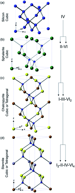
TMC semi-conductors that are suitable for photovoltaic devices cover a staggeringly large range of materials (at least 15![[thin space (1/6-em)]](https://www.rsc.org/images/entities/char_2009.gif) 000 different compounds according to a search of the ICSD). These classes can be broken down into three main categories: binary (MxEn), ternary (MxM′yEn) and quaternary (MxM′yM′′zEn) (where M = transition metal, M′/M′′ = transition or other metal and E = S, Se or Te) systems (Fig. 1). The classes are often described in Roman numerals, with the numeral referring to the oxidation state of the metal and the group of the chalcogen or pnictogen, e.g. II–VI (CdS), I–III–VI2 (CuInS2) or III–V (InP).
000 different compounds according to a search of the ICSD). These classes can be broken down into three main categories: binary (MxEn), ternary (MxM′yEn) and quaternary (MxM′yM′′zEn) (where M = transition metal, M′/M′′ = transition or other metal and E = S, Se or Te) systems (Fig. 1). The classes are often described in Roman numerals, with the numeral referring to the oxidation state of the metal and the group of the chalcogen or pnictogen, e.g. II–VI (CdS), I–III–VI2 (CuInS2) or III–V (InP).
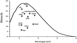
One requirement for a good photoactive semiconductor is that it must have a band gap between 1.0–1.5 eV between the lower lying valence band and the higher energy conduction band. This is a consequence of the Shockley–Quessier (SQ) limit, which is the theoretical maximum efficiency for a single pn-junction solar cell. Fig. 2 shows the SQ limit for semiconductors under the standard atmospheric solar emission spectrum (with an air mass of coefficient of 1.5 and a solar zenith angle of 48.19°, i.e. AM 1.5), demonstrating that the maximum photoconversion efficiency lies in the 1.0–1.5 eV region.15
The principles behind the photoactivity of TMC semiconductors can be understood by considering layered binary systems. Group IV dichalcogenides, such as ZrS2 and HfS2, have an analogous electronic structure to TiO2, i.e. a valence band derived from S-p orbitals and a conduction band of Zr/Hf-d orbitals. For the other TMCs the metal has electrons in the d-orbitals: these occupy states that lie between the E-p orbital and the empty M-d orbitals. For the ternary and quaternary systems that do not adopt a layered structure, an appropriate example is CZTS (Cu2ZnSnS4). In this case the upper valence band consists of hybridised S-p and Cu-d orbitals, while the conduction band is derived from the hybridisation of S-s/p and Sn-s orbitals.16
TMC semiconductors are beginning to realise their potential as building blocks in photovoltaic devices based on thin films,17 quantum dots (QD),18 and dye-sensitized solar cells (DSSC).19 One of the major challenges that face researchers is to find a semiconductor material with a band gap in the range 1.0–1.5 eV and with a high absorption coefficient that can be made cheaply from elements that are plentiful. Fortunately there are many choices of TMC that fit these criteria, though some have shortcomings that will be discussed below. This perspective will seek to highlight the key TMCs that offer the greatest potential for commercialisation and will discuss the properties and synthetic routes toward these materials.
Synthetic routes to devices
Transition metal chalcogenides have found a number of uses in PV devices, ranging from photoabsorber layers to buffer layers and anodes in DSSCs. The form they take in these devices is generally either as a nanostructured thin film or as quantum dots.The manufacture of thin films can be split into three rather broad sections: chemical vapour deposition, atomic deposition or solution processing. These broad sections encompass a wide variety of techniques that have each earned an acronym in their own right, but can be collated based on a basic similar principle.
Chemical vapour deposition (CVD), in all its major forms including metal–organic CVD (MO-CVD), and low pressure CVD, (LP-CVD) involves the decomposition of a precursor in the gas phase leading to the growth of a substrate on a target. The CVD process has been used extensively by researchers to generate high quality thin films.20–24 The range of suitable precursors is large, with many options available as to whether individual components or single source precursors are used. Techniques such as aerosol assisted CVD (AA-CVD) have been developed to circumvent the need for volatile precursors and as such widens the scope of precursors available for materials fabrication.25
Atomic deposition encompasses a broad range of techniques, but the purpose of these in general is to deposit a layer of the individual components that are then later annealed in the presence of elemental chalcogen. The deposition techniques include atomic layer deposition (ALD),26 successive ionic layer adsorption and reaction (SILAR),27 sputtering28 and pulsed laser deposition.29 The advantages of processes such as ALD are precise thickness control at the monolayer level, which can be important for optimising device performance. The disadvantages of these processes are that they are not suitable for manufacturing large scale devices, often require ultra-high vacuum with the associated complications, and at the laboratory level are often custom builds, leading to difficulties in reproducing results from one instrument to another.
Solution processing of TMCs can include the synthesis of nanocrystalline material, which may be treated as an ‘ink’ and processed into a film,30,31 or processes such as chemical bath deposition (CBD).32,33 Nanocrystalline TMCs have been synthesised by the ubiquitous hot-injection route, which has proven to be applicable to binary, ternary and quaternary systems, as well as others such as solvothermal syntheses.
Binary systems
Binary transition metal chalcogenides have the form MxEn (M transition metal, E = S, Se, Te). There are a vast range of binary TMC systems that have demonstrate suitable properties for photovoltaic systems, including: FeS2,34,35 CdS,36 CuxS,37,38 CuSe,39 MoS2,40,41 RuS2,42–45 ZrS2/Se2,46 TaS2 (ref. 47) and AgS.48Amongst these systems Cd(S,Se), FeS2 and the various copper sulfides demonstrate the most exciting properties and are perhaps the most well-known.
Cadmium sulfide/selenide quantum dots were almost ubiquitous in the early 2000s, as facile routes has been developed for their synthesis in the preceding decade49–51 and had ideal photoelectric properties. The electronic properties of the Cd(S,Se) quantum dots, notably the band gap, can be easily tuned by controlling the proportion of sulfur/selenium.52 However, cadmium has a well-documented high toxicity,53,54 which has led to strict EU regulation. This in theory limits the suitability of cadmium chalcogenides as a photovoltaic for anything other than a laboratory scale test. Cd solar cells are however still being developed and in 2016 First Solar set a new record efficiency of 22.1% for CdTe with a thin film device.55
FeS2, pyrite (or Fool's Gold) has a band gap of 0.95 eV and an absorption coefficient of 105 cm−1. Combining this with the extremely low raw material costs and simplicity of synthesis56 at face value pyrite should make an excellent candidate for PV devices. Indeed, nanostructured FeS2 has been used in DSSCs, as a photoconductor, in a p–i–n heterojunction and in bulk heterojunction inorganic–organic hybrid solar cells.57–60 However, it seems that surface defects brought upon by sulfur vacancies can severely affect the electronic properties. Steinhagen et al. have shown that nanocrystal devices are particularly prone to this owing to the high concentration of grain boundaries and presumably the high fraction of atoms that reside at the surface in nanoscale particles.34 Shukla et al. demonstrated that photovoltages can be obtained from pyrite nanocubes by sulfurizing a deposited colloidal ink. They conclude that surface defects are the major contribution to hole–electron recombination (Fig. 3) and increased efficiency may be obtained either by reducing the grain boundaries or reducing defects through an improved synthetic route.35
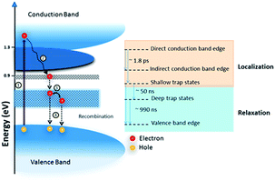 | ||
| Fig. 3 Origin of the loss of charge carriers in FeS2. (1) An electron is optically excited from the valence to the conduction band, (2) the charge carrier is rapidly localized at the indirect band edge and low lying shallow defect states, (3) slower electron relaxation to long lived trap states, and (4) electron–hole recombination. Reprinted with permission from ref. 35, ©2016 American Chemical Society. | ||
Ruthenium sulfide adopts the same pyrite structure as FeS2, and like iron sulfide, has an appropriate (though indirect) band gap of 1.3 eV. Single crystals of RuS2 have been shown to oxidise H2O upon illumination, but it is thought that RuO2 is probably responsible.42 The single crystals show a limited photocurrent, but deposited thin films do not, possibly due to a high electron/hole re-trapping and combination rate.44,45
Copper sulfide exists in a large number of phases related to the stoichiometry of CuxS, which all have a band gap in the region of 1.2–2.0 eV.37 For x < 2, the band gap is closer to 2.0 eV and so these are of limited use in PV applications, however Cu2S is an indirect band gap semiconductor with a bulk band gap of 1.21 eV,38 its selenide analogue, Cu2Se, has an indirect band gap of 1.4 eV.39 Cu2S was widely used in combination with CdS in the 1960s–1980s61 but diffusion of Cu+ ions into the CdS layer degraded the PV cell over time. Wu et al. reported the synthesis of Cu2S nanocrystals from the reaction of copper(II) acetylacetonate and ammonium diethyldithiocarbamate in a mixed solvent of dodecanethiol and oleic acid. They then spin coated these nanocrystals onto a layer of CdS nanorods to produce a PV device of with an efficiency of 1.6%.38 Mousavi-Kamazani have since deposited it on TiO2 as part of a DSSC to improve the efficiency to 8.3%.62
Also in group 11, both AgS and Ag2S have band gaps ∼1.1 eV,48,63 which should give them both appealing PV characteristics. However, few serious attempts have been made to optimise a silver sulfide based solar cell. Tubtimtae63 and Shen64 have both tested devices, with the former achieving an efficiency of 1.70%.
MoS2 is a layered TMC that has seen a substantial amount of recent research owing to its ability to exist in monolayer form.1 It has a direct band gap of 1.85 eV in its monolayer and an indirect band gap of 1.2 eV in the bulk. The band gap is related to the number of layers of MoS2 and so it is a strong candidate for PV applications, as the band gap can be tuned by controlling the thickness.65 Gourmelon et al. and Shanmugam et al. have both reported the use of MoS2 in solar cells to give an efficiency of 1.3%,40,66 whilst Gong et al. have shown that the band gap can be further tuned by the introduction of selenium.41 One potential problem for molybdenum sulfide in the thermodynamically stable 2H–MoS2 structure is that poor alignment of the layers can drastically reduce the photosensitivity. The Van der Waals planes between the monolayer sheets of 2H–MoS2 contain a high concentration of defects, which can trap charge carriers. If a high photoconversion efficiency is to be achieved then these must be reduced. Indeed, efforts have recently been directed to ameliorate these defects using the organic superacid bis(trifluoromethane)sulfonamide, which led to the almost complete suppression of non-radiative recombination and a photoluminescence quantum yield improvement from 0.6% to 95%, which paves the way to the use of 2D MoS2 in photovoltaic devices.67 This approach has been extended to WS2, though does not work for MoSe2 or WSe2.68
The ZrSxSe2−x family has been grown by Moustafa et al., and the band gap range found to be 1.18 eV (ZrSe2) to 1.7 eV (ZrS2).46 This suggests that zirconium selenide should be tested for PV characteristics, though to the best of our knowledge this has not been carried out.
Manganese(II) sulfide has been used as a dopant in PbS, CdS, CdSe and ZnS quantum dots,69 with a PV conversion efficiency of 4.25% demonstrated in a PbS quantum dot DSSC by Punnoose et al.70 It has not, however, been used as the photoabsorber by itself as it has a band gap of 3.1 eV.71
Typically a DSSC has a platinum counter electrode (Fig. 4), and a significant amount of research has been directed to reducing this reliance on noble metals. Naturally, some attention has been bestowed on carbon materials (graphene, nanotubes, carbon black),72 but molybdenum,73 nickel74 and cobalt sulfides75 have also been investigated. In a related manner, tantalum sulfide nanosheets with a band gap of 1.92 eV are promising candidates for electrodes in organic photovoltaic (OPV) devices.47
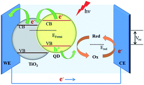 | ||
| Fig. 4 A schematic of a quantum dot (QD) sensitized solar cell (QDSSC). The QD is photoexcited and transfers an electron to TiO2 on an indium tin oxide (ITO) working electrode (WE). The electrolyte undergoes a redox cycle on the counter electrode (CE) for which metal chalcogenides have been proposed. Reprinted with permission from ref. 19, ©2015 Royal Society of Chemistry. | ||
On a final note, a main group binary chalcogenide that has attracted interest for photovoltaics is tin monosulfide (SnS), due to its band gap commensurate with solar absorption (typically 1.1–1.4 eV),76 with a theoretical power conversion efficiency of up to 24%. Gordon and co-workers demonstrated a PV cell with record efficiency of 4.4%,77 and thus there is great room for improvement. Efforts in our group have focused on using AACVD to fabricate these semiconductors as thin films suitable for eventual use in PV device architectures.78–80 Interestingly, SnS is a Van der Waals layer structure, and we have shown that thinning these materials to the 2D limit can control the band gap energy in a predictable manner that is layer dependent in nature.81
Ternary
When the metal of a binary metal chalcogenide system is substituted for two metals providing the same total charge and hence is isoelectric, i.e. moving from MxEn (Fig. 1b) to MxM′yEn (Fig. 1c), a new category of ternary metal chalcogenides is accessed. The use of two different metals allows access to the band gaps and not accessible to binary metal chalcogenides. A common ternary system possesses two metals each with oxidation states of +1 and +3 in combination with a pair of chalcogens each in oxidation state −2. This is described as a I–III–VI2e.g. CuInS2. The parent binary system to I–III–VI2 is the II–VI system where CdSe is an example (Fig. 1). Systems where there are two different chalcogens, i.e. MxM′yEnE′m, also fall under the general I–III–VI2 system and are classified as ternary systems despite containing four separate elements. In an identical fashion to their parent binary systems, ternary systems also undergo quantum confinement and behave as quantum dots.82 Utilising the energy modulation effects by manifestation of quantum confinement in these materials allows ternary metal chalcogenides to access the entire solar spectrum which is highly beneficial for light harvesting and makes them an attractive alternative to toxic binary metal chalcogenides like cadmium chalcogenides (Fig. 5).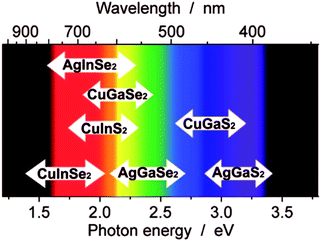 | ||
| Fig. 5 An illustration of the visible spectrum and where some typical chalcopyrite-type I–III–VI2 nanocrystals absorb when between 2 and 5 nm in size. Reprinted with permission from ref. 82, ©2009 American Institute of Physics. | ||
The chalcopyrite phase of copper indium sulfide, CuInS2 (often abbreviated to CIS) is a ternary metal chalcogenide that has been explored as a component of heterojunction PV devices. CuInS2 is a useful material for use in photovoltaic devices due to a direct band gap of 1.5 eV, an absorption coefficient >105 cm−1, tolerance to defects and high radiation hardness.83 Early devices used CIS in combination with CdS or InP and homojunction devices in the 1970's.84–86 The growth conditions of the CuInS2 and resulting defects also govern if it is an n- or p-type semiconductor, depending on if it is formed in an indium or sulfur rich environment respectively (Fig. 6).87,88 The high proportion of defects also leads to advantageous properties such as the ability to take a high loading of dopants and band gap tuning through the number of defect sites.89,90 Although useful, these properties can also lead to compositional differences between nanocrystals of identical size within a batch leading to broadening on the ensemble properties such as the luminescence peak of colloidal nanocrystals.91
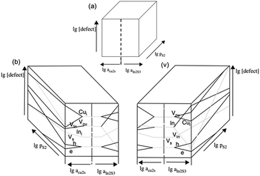 | ||
| Fig. 6 (a) The 3D concept of a Brouwer diagram for CIS, i.e. how a change in stoichiometry (in Cu, In or S) results in defects in (b) a Cu-rich regime and (c) an In-rich regime. Adapted with permission from ref. 88, ©2008 Springer. | ||
The difficulty in forming phase pure CuInE2 lies in that Cu(I) is a soft Lewis acid whereas In(III) is a hard Lewis acid. As a consequence their reactivity towards the sulfur precursor, often a Lewis base, is different. Accordingly the formation of CuxSy phases is a common observation whilst optimising synthetic routes.92 Thus balancing the reactivity of the precursors used at the same time complicates the optimisation of the synthetic strategies towards CuInS2. The resulting nanocrystals often differ from the ideal C![[thin space (1/6-em)]](https://www.rsc.org/images/entities/char_2009.gif) :
:![[thin space (1/6-em)]](https://www.rsc.org/images/entities/char_2009.gif) I
I![[thin space (1/6-em)]](https://www.rsc.org/images/entities/char_2009.gif) :
:![[thin space (1/6-em)]](https://www.rsc.org/images/entities/char_2009.gif) S elemental ratio of 1
S elemental ratio of 1![[thin space (1/6-em)]](https://www.rsc.org/images/entities/char_2009.gif) :
:![[thin space (1/6-em)]](https://www.rsc.org/images/entities/char_2009.gif) 1
1![[thin space (1/6-em)]](https://www.rsc.org/images/entities/char_2009.gif) :
:![[thin space (1/6-em)]](https://www.rsc.org/images/entities/char_2009.gif) 2 thus allowing another degree of control over the properties of the nanocrystals produced. The phase diagram of CuInS2 is complex and at below 800 °C the window to form CuInS2 is narrow (Fig. 7).93
2 thus allowing another degree of control over the properties of the nanocrystals produced. The phase diagram of CuInS2 is complex and at below 800 °C the window to form CuInS2 is narrow (Fig. 7).93
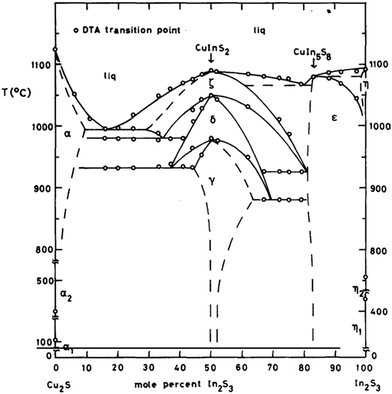 | ||
| Fig. 7 Tentative diagram of the T–x relations along the join Cu2S–In2S3 at moderate pressure(s). The single phase regions are indicated by their respective symbol. The two phase regions, which lie in between the single phase regions are not indicated. The gamma phase is the target CuInS2 chalcopyrite phase. Reprinted with permission from ref. 88, ©1980 Elsevier. | ||
The Bohr radius of CuInS2 is ca. 4.1 nm and thus CIS undergoes quantum confinement when nanocrystals are below 8.2 nm. This allows CuInS2 to absorb the entire visible region of the solar spectrum by control of the size of the nanocrystals used (Fig. 8).92
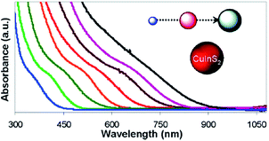 | ||
| Fig. 8 Absorption spectra of CIS nanocrystals of different sizes between 2 and 16 nm reprinted with permission from ref. 92, ©2013 American Chemical Society. | ||
As previously described, the composition can be varied from the ideal 1![[thin space (1/6-em)]](https://www.rsc.org/images/entities/char_2009.gif) :
:![[thin space (1/6-em)]](https://www.rsc.org/images/entities/char_2009.gif) 1
1![[thin space (1/6-em)]](https://www.rsc.org/images/entities/char_2009.gif) :
:![[thin space (1/6-em)]](https://www.rsc.org/images/entities/char_2009.gif) 2 of CuInS2. Altering the Cu
2 of CuInS2. Altering the Cu![[thin space (1/6-em)]](https://www.rsc.org/images/entities/char_2009.gif) :
:![[thin space (1/6-em)]](https://www.rsc.org/images/entities/char_2009.gif) In ratio causes the position of the valence band to change as it is composed of S-3p and Cu-3d orbitals. In copper poor nanocrystals the valence band falls and the bandgap widens (Fig. 9).94
In ratio causes the position of the valence band to change as it is composed of S-3p and Cu-3d orbitals. In copper poor nanocrystals the valence band falls and the bandgap widens (Fig. 9).94
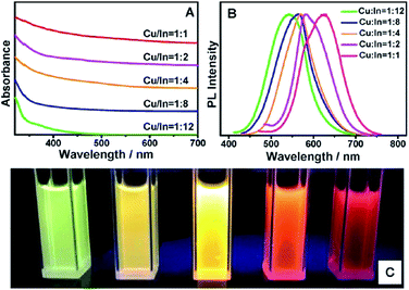 | ||
Fig. 9 (a) Absorption and (b) fluorescence spectra of CIS nanoparticles with different Cu![[thin space (1/6-em)]](https://www.rsc.org/images/entities/char_2009.gif) : :![[thin space (1/6-em)]](https://www.rsc.org/images/entities/char_2009.gif) In ratio and (c) a picture of the corresponding solutions under UV irradiation. Reprinted with permission from ref. 94, ©2013 American Chemical Society. In ratio and (c) a picture of the corresponding solutions under UV irradiation. Reprinted with permission from ref. 94, ©2013 American Chemical Society. | ||
In the same manner as CuInS2, CuInSe2 can also be an n- or p-type semiconductor depending on the abundances of In or Se.95 With a band gap of 1.02 eV, it has sub-optimal absorption characteristics with respect to the AM 1.5 solar emission spectrum in the bulk as-compared with CuInS2 but, on the other hand, has a very high absorption coefficient of 105 cm−1 making it a good candidate for PV devices.96 As with CuInS2, the band gap of CuInSe2 can be controlled by altering the size and composition of the nanocrystals. CuInSe2 also undergoes strong quantum confinement compared to other copper based ternary metal chalcogenides, ranging from 1.0 eV for 6 nm particles to 3.2 eV at 1 nm particle diameter.82
Copper gallium selenide is also a I–III–VI2 ternary metal chalcogenide with the chalcopyrite structure. It possess a direct band gap of 1.66 eV and possesses a high optical absorption coefficient (105 cm−1).97 The use of CuGaSe2 in photovoltaics has been hindered by the difficulty in producing a single phase material. In response to this there have been new synthetic routes to the formation of phase pure CuGaSe2 through colloidal routes.98,99
Unlike CuGaSe2, CuGaS2 has undergone far less investigation due to greater difficulty in the growth of a single phase. Bulk CuGaS2 possesses a direct band gap of 2.49 eV allowing for use in the visible (green) region of the electromagnetic spectrum.100 As with CIS there is a tendency to form intrinsic defects (caused by Cu vacancies and Ga substitution of Cu atoms) which greatly influence the observed properties of the material produced.101
The antimony analogue chalcostibite (CuSbS2) is a relatively under-studied compound, though has an appropriate direct band gap of 1.38–1.50 eV.102–104 It has the added benefit of composed of earth abundant and non-toxic elements, though phase pure CuSbS2 is hard to achieve owing to contamination of other copper antimony sulfide phases or binary impurities such as Cu2S and Sb2S3.105
For the I–III–VI2 chalcopyrite-type compounds described above, copper has been exchanged for silver as AgInS2,106 AgInSe2,107 AgGaS2,108 and AgGaSe2.109 The silver analogues have similar properties to the Cu compounds, but can be synthesised under milder conditions.106 The replacement of cheap copper with relatively expensive silver is unlikely to aid the industrial uptake of this class of material. However, as the material is used in thin film form the total silver required is miniscule and the ability to form phase pure films is a significant advantage.
A very different class of compound, the transition metal chalcogenide perovskite has been identified by density functional theory (DFT) as being a target of interest.110 Ammonium lead halide perovskites have become an extremely highly studied area that shows great promise,111–113 but the presence of toxic Pb is a concern for widespread uptake. Sun et al., have proposed CaTiS3, BaZrS3, BaZrSe3 and CaHfSe3 as potential candidates.110 Limited experimental work has been undertaken on these compounds, and a second DFT study has indicated that they might present significant synthetic challenges.114
Quaternary
Quaternary transition metal chalcogenide systems, i.e. those with a general formula MxM′yM′′zEn (M = transition metal, M′/M′′ = transition or other metal and E = S, Se or Te), are amongst the most challenging to synthesise, but offer the greatest potential for highest efficiencies.There are two major quaternary systems that have been substantially studied: copper indium gallium selenide [CIGS, Cu(In,Ga)Se2] and copper zinc tin sulfide/selenide [CZTS, Cu2ZnSn(S,Se)4]. The CIGS system is an established technology that has seen commercial application, whilst the CZTS one remains at the R&D stage.
Chalcopyrite-based solar cells were first developed using CuInSe2 as the absorber material, which has a band gap of 1.04 eV. However, it was discovered that the band gap could be tuned by adding gallium in place of indium to a maximum of 1.68 eV (for CuGaSe2). Optimisation of devices has led to the conclusion that a Ga/(Ga + In) ratio of 0.25–0.35 (i.e. CuIn0.75Ga0.25Se2) gives devices with optimal power conversion efficiencies. This corresponds to a band gap of 1.10–1.25 eV.115
CIGS is one of the few transition metal chalcogenide photovoltaics to have been commercialised, with a number of companies marketing devices with >15% efficiency.115 It has a number of attractive properties, which include benign grain boundaries and a tolerant phase diagram that allows for a variety in composition whilst maintaining phase.116
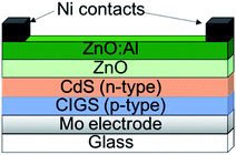
In a typical CIGS device, Cu(In,Ga)Se2 is deposited on a Mo coated substrate, either by sputtering116 or through a solution process.117 At this stage Na or K are introduced as this improves the electronics of the device.118,119 On top of this a CdS buffer layer is grown (often by chemical bath deposition), followed by n-type ZnO/Al:ZnO transparent conducting windows. In some cases the CdS has been replaced with ZnS for a more environmentally friendly system.120 This leads to a typical device layout shown in Fig. 10.
The use of CIGS is undoubtedly a success in terms of efficiency, ease of manufacture and presence in the market, however, it has one major drawback which is shared by the ternary CIS (and its related family): availability of indium. The British Geological Survey ranks In as a ‘high supply risk’ in its 2015 Risk List.12 This has encouraged workers to turn to Cu2ZnSnS4 (CZTS) as an earth abundant, cheap and environmentally benign photovoltaic material.
CZTS has a high absorption coefficient and a direct band gap of 1.45 eV which may be tuned by controlling the stoichiometry of the material.121 The current record efficiency is a very commendable 12.6%,122 indicating the great potential of this material. As with CIGS, it is often prepared through a sputtering or vapour deposition process, with a high temperature annealing step. There are two challenges that arise from this high temperature annealing step that must be overcome before CZTS becomes commercially viable. Firstly, the photoconversion efficiency of CZTS absorber layers is dependent upon the stoichiometry of the material, and during the annealing step volatile compounds such as SnS may be lost. This makes it difficult to control the composition of the target phase.28,123–126 Indeed, solar cells made from Cu poor films perform substantially better than those made from stoichiometric Cu2ZnSnS4.123 The second challenge is that the Mo electrode that CZTS is often deposited on can react with sulfur to form a MoS2 layer between electrode and absorber (Fig. 11), leading to a drastic loss of efficiency.127–129
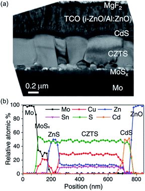 | ||
| Fig. 11 A cross-section of a typical CZTS device reveals the atomic composition of the different layers. (a) SEM image of a cross-section and (b) elemental composition determined by EDX as a function of position from the Mo contact. Reprinted with permission from ref. 129, ©2011 John Wiley & Sons, Ltd. | ||
There are further challenges in the fundamental materials science associated with CZTS as it can potentially exist in three stable phases (kesterite, stannite and a primitive mixed CuAu-like structure).16,130,131 The presence of these can influence the optical and electronic properties of the material. Additionally, the phase diagram for CZTS is not as tolerant as for CIGS and negative contamination with binary or ternary phases is likely.121
Despite these challenges, CZTS is one of the most viable transition metal chalcogenides for extensive industrial applications, owing to its cheap, abundant and non-toxic components. The highest efficiency devices of this class have come from solution processing methods, suggesting that this might be the best route to explore in the future.122,132
Future outlook
The requirement for renewable energy sources remains a major research challenge at the present. Efficient and cheap photovoltaic materials are needed to tackle this challenge, and transition metal chalcogenides provide a viable route to this objective. Amongst ternary and quaternary systems some stand out candidates represent major targets for the future. CuInS2, Cu(In,Ga)S2 and Cu2ZnSnS4 are the three materials that are most likely to have a major impact. However, there are major concerns about the long term availability of indium and gallium, suggesting that alternatives must be sought. This leaves CZTS as the best hope. For it to fulfil its potential efforts must be directed to improve the manufacturing process, as this is a major source of the limits on its efficiency. Binary materials, such as Cu2S and FeS2, offer the greatest potential return when balancing theoretical energy conversion against cost. The challenge here is to produce large amounts of high quality, phase pure material.Acknowledgements
The authors acknowledge funding from the EPSRC with grants EP/K010298/1 and EP/K039547/1 (POB and PDMcN) and a Doctoral Prize for PDM. POB and PDMcN also thank The Royal Society DFID Africa Capacity Building Schemes for their financial support.Notes and references
- A. A. Tedstone, D. J. Lewis and P. O'Brien, Chem. Mater., 2016, 28, 1965–1974 CrossRef CAS.
- N. Savjani, E. A. Lewis, M. A. Bissett, J. R. Brent, R. A. W. Dryfe, S. J. Haigh and P. O'Brien, Chem. Mater., 2016, 28, 657–664 CrossRef CAS.
- N. Savjani, E. A. Lewis, R. A. D. Pattrick, S. J. Haigh and P. O'Brien, RSC Adv., 2014, 4, 35609–35613 RSC.
- H. Wang, H. Yuan, S. Sae Hong, Y. Li and Y. Cui, Chem. Soc. Rev., 2015, 44, 2664–2680 RSC.
- S.-L. Li, K. Tsukagoshi, E. Orgiu and P. Samorì, Chem. Soc. Rev., 2015, 45, 118–151 RSC.
- X. Chia, A. Y. S. Eng, A. Ambrosi, S. M. Tan and M. Pumera, Chem. Rev., 2015, 115, 11941–11966 CrossRef CAS PubMed.
- C. Tan and H. Zhang, Chem. Soc. Rev., 2015, 44, 2713–2731 RSC.
- H. Yu, W. Yao and X. Xu, Nat. Rev. Mater., 2016, 1, 16055 CrossRef.
- W. R. Mateker and M. D. McGehee, Adv. Mater., 2017, 29, 1603940 CrossRef PubMed.
- D. Li, P. Liao, X. Shai, W. Huang, S. Liu, H. Li, Y. Shen and M. Wang, RSC Adv., 2016, 6, 89356–89366 RSC.
- J.-P. Correa-Baena, A. Abate, M. Saliba, W. Tress, T. J. Jacobsson, M. Gratzel and A. Hagfeldt, Energy Environ. Sci., 2017 10.1039/C6EE03397K.
- (a) British Geological Survey, Risk List 2015, BGS, Nottingham, 2015 Search PubMed; (b) British Geological Survey, Risk List 2015, https://www.bgs.ac.uk/downloads/start.cfm?id=3075, accessed March 2017 Search PubMed.
- C. Wadia, A. P. Alivisatos and D. M. Kammen, Environ. Sci. Technol., 2009, 43, 2072–2077 CrossRef CAS PubMed.
- US Geological Survey, Mineral Commodity Summaries 2017, US Geological Survey, Virginia, 2017 Search PubMed.
- P. K. Nayak and D. Cahen, in Advanced Concepts in Photovoltaics, ed. A. J. Nozik, G. Conibeer and M. C. Beard, The Royal Society of Chemistry, Cambridge, 2014, pp. 547–566 Search PubMed.
- S. Chen, X. G. Gong, A. Walsh and S. H. Wei, Appl. Phys. Lett., 2009, 94, 25–27 Search PubMed.
- X. Liu, Y. Feng, H. Cui, F. Liu, X. Hao, G. Conibeer, D. B. Mitzi and M. Green, Prog. Photovoltaics, 2016, 24, 879–898 Search PubMed.
- I. Gur, N. A. Fromer, M. L. Geier and A. P. Alivisatos, Science, 2005, 310, 462–466 CrossRef CAS PubMed.
- K. Meng, G. Chen and K. R. Thampi, J. Mater. Chem. A, 2015, 3, 23074–23089 CAS.
- K. Ramasamy, M. A. Malik and P. O'Brien, Chem. Sci., 2011, 2, 1170–1172 RSC.
- M. A. Malik, M. Afzaal and P. O'Brien, Chem. Rev., 2010, 110, 4417–4446 CrossRef CAS PubMed.
- L. S. Price, I. P. Parkin, A. M. E. Hardy, R. J. H. Clark, T. G. Hibbert and K. C. Molloy, Chem. Mater., 1999, 11, 1792–1799 CrossRef CAS.
- A. Govind Rajan, J. H. Warner, D. Blankschtein and M. S. Strano, ACS Nano, 2016, 10, 4330–4344 CrossRef CAS PubMed.
- R. S. Mane and C. D. Lokhande, Mater. Chem. Phys., 2000, 65, 1–31 CrossRef CAS.
- P. Marchand, I. A. Hassan, I. P. Parkin and C. J. Carmalt, Dalton Trans., 2013, 42, 9406–9422 RSC.
- S. M. George, Chem. Rev., 2010, 110, 111–131 CrossRef CAS PubMed.
- H. M. Pathan and C. D. Lokhande, Bull. Mater. Sci., 2004, 19, 85–111 CrossRef.
- Y. Feng, B. Yu, G. Cheng, T. Lau, Z. Li, L. Yin, Q. Song, C. Yang and X. Xiao, J. Mater. Chem. C, 2015, 3, 9650–9656 RSC.
- K. Moriya, K. Tanaka and H. Uchiki, Jpn. J. Appl. Phys., 2008, 47, 602–604 CrossRef CAS.
- J. Puthussery, S. Seefeld, N. Berry, M. Gibbs and M. Law, J. Am. Chem. Soc., 2011, 133, 716–719 CrossRef CAS PubMed.
- Q. Guo, H. W. Hillhouse and R. Agrawal, J. Am. Chem. Soc., 2009, 131, 11672–11673 CrossRef CAS PubMed.
- P. O'Brien and J. Mcaleese, J. Mater. Chem., 1998, 8, 2309–2314 RSC.
- D. S. Boyle, A. Bayer, M. R. Heinrich, O. Robbe and P. O'Brien, Thin Solid Films, 2000, 361, 150–154 CrossRef.
- C. Steinhagen, T. B. Harvey, C. J. Stolle, J. Harris and B. A. Korgel, J. Phys. Chem. Lett., 2012, 3, 2352–2356 CrossRef CAS PubMed.
- S. Shukla, G. Xing, H. Ge, R. R. Prabhakar, S. Mathew, Z. Su, V. Nalla, T. Venkatesan, N. Mathews, T. Sritharan, T. C. Sum and Q. Xiong, ACS Nano, 2016, 10, 4431–4440 CrossRef CAS PubMed.
- D. C. Reynolds, G. Leies, L. L. Antes and R. E. Marburer, Phys. Rev., 1954, 96, 533–534 CrossRef CAS.
- I. Grozdanov and M. Najdoski, J. Solid State Chem., 1995, 114, 469–475 CrossRef CAS.
- Y. Wu, C. Wadia, W. Ma, B. Sadtler and A. P. Alivisatos, Nano Lett., 2008, 8, 2551–2555 CrossRef CAS PubMed.
- S. Deka, A. Genovese, Y. Zhang, K. Miszta, G. Bertoni, R. Krahne, C. Giannini and L. Manna, J. Am. Chem. Soc., 2010, 132, 8912–8914 CrossRef CAS PubMed.
- E. Gourmelon, O. Lignier, H. Hadouda, G. Couturier, J. C. Bernède, J. Tedd, J. Pouzet and J. Salardenne, Sol. Energy Mater. Sol. Cells, 1997, 46, 115–121 CrossRef CAS.
- Y. Gong, Z. Liu, A. R. Lupini, G. Shi, J. Lin, S. Najmaei, Z. Lin, A. L. Elias, A. Berkdemir, G. You, H. Terrones, M. Terrones, R. Vajtai, S. T. Pantelides, S. J. Pennycook, J. Lou, W. Zhou and P. M. Ajayan, Nano Lett., 2014, 14, 442–449 CrossRef CAS PubMed.
- A. M. Chaparro, N. Alonso-Vante, P. Salvador and H. Tributsch, J. Electrochem. Soc., 1997, 144, 2991–2996 CrossRef CAS.
- M. Ashokkumar, A. Kudo, N. Saito and T. Sakata, Chem. Phys. Lett., 1994, 229, 383–388 CrossRef CAS.
- P. Bogdanoff, C. Zachäus, S. Brunken, A. Kratzig, K. Ellmer and S. Fiechter, Phys. Chem. Chem. Phys., 2013, 15, 1452–1459 RSC.
- S. Brunken, A. Kratzig, P. Bogdanoff, S. Fiechter and K. Ellmer, Thin Solid Films, 2013, 527, 16–20 CrossRef CAS.
- M. Moustafa, T. Zandt, C. Janowitz and R. Manzke, Phys. Rev. B: Condens. Matter Mater. Phys., 2009, 80, 35206 CrossRef.
- Q. Van Le, T. P. Nguyen, K. S. Choi, Y.-H. Cho, Y. J. Hong and S. Y. Kim, Phys. Chem. Chem. Phys., 2014, 16, 25468–25472 RSC.
- K. Akamatsu, S. Takei, M. Mizuhata, A. Kajinami, S. Deki, S. Takeoka, M. Fujii, S. Hayashi and K. Yamamoto, Thin Solid Films, 2000, 359, 55–60 CrossRef CAS.
- T. Trindade and P. O. Brien, Chem. Mater., 1997, 9, 523–530 CrossRef CAS.
- B. O. Dabbousi, J. Rodriguez, F. V. Mikulec, J. R. Heine, H. Mattoussi, R. Ober, K. F. Jensen and M. G. Bawendi, J. Phys. Chem. B, 1997, 101, 9463–9475 CrossRef CAS.
- D. R. Larson, W. R. Zipfel, R. M. Williams, S. W. Clark, M. P. Bruchez, F. W. Wise and W. W. Webb, Science, 2003, 300, 1434–1436 CrossRef CAS PubMed.
- P. K. Santra and P. V. Kamat, J. Am. Chem. Soc., 2013, 135, 877–885 CrossRef CAS PubMed.
- P. Das, S. Samantaray and G. R. Rout, Environ. Pollut., 1997, 98, 29–36 CrossRef CAS PubMed.
- J. Godt, F. Scheidig, C. Grosse-Siestrup, V. Esche, P. Brandenburg, A. Reich and D. A. Groneberg, J. Occup. Med. Toxicol., 2006, 1, 22 CrossRef PubMed.
- M. A. Green, K. Emery, Y. Hishikawa, W. Warta and E. D. Dunlop, Prog. Photovoltaics, 2016, 24, 905–913 Search PubMed.
- P. D. Matthews, M. Akhtar, M. A. Malik, N. Revaprasadu and P. O'Brien, Dalton Trans., 2016, 45, 18803–18812 RSC.
- D. Y. Wang, Y. T. Jiang, C. C. Lin, S. S. Li, Y. T. Wang, C. C. Chen and C. W. Chen, Adv. Mater., 2012, 24, 3415–3420 CrossRef CAS PubMed.
- Y. C. Wang, D. Y. Wang, Y. T. Jiang, H. A. Chen, C. C. Chen, K. C. Ho, H. L. Chou and C. W. Chen, Angew. Chem., Int. Ed., 2013, 52, 6694–6698 CrossRef CAS PubMed.
- A. Kirkeminde, R. Scott and S. Ren, Nanoscale, 2012, 7649–7654 RSC.
- Z. Yang, M. Wang, S. Shukla, Y. Zhu, J. Deng, H. Ge, X. Wang and Q. Xiong, Sci. Rep., 2015, 5, 11377 CrossRef CAS PubMed.
- K. W. Boer, J. Cryst. Growth, 1982, 59, 111–120 CrossRef.
- M. Mousavi-Kamazani, Z. Zarghami and M. Salavati-Niasari, J. Phys. Chem. C, 2016, 120, 2096–2108 CAS.
- A. Tubtimtae, K. L. Wu, H. Y. Tung, M. W. Lee and G. J. Wang, Electrochem. Commun., 2010, 12, 1158–1160 CrossRef CAS.
- H. Shen, X. Jiao, D. Oron, J. Li and H. Lin, J. Power Sources, 2013, 240, 8–13 CrossRef CAS.
- K. F. Mak, C. Lee, J. Hone, J. Shan and T. F. Heinz, Phys. Rev. Lett., 2010, 105, 136805 CrossRef PubMed.
- M. Shanmugam, T. Bansal, C. A. Durcan and B. Yu, Appl. Phys. Lett., 2012, 100, 153901 CrossRef.
- M. Amani, D.-H. Lien, D. Kiriya, J. Xiao, A. Azcatl, J. Noh, S. R. Madhvapathy, R. Addou, S. Kc, M. Dubey, K. Cho, R. M. Wallace, S.-C. Lee, J.-H. He, J. W. Ager III, X. Zhang, E. Yablonovitch and A. Javey, Science, 2015, 350, 1065–1068 CrossRef CAS PubMed.
- M. Amani, P. Taheri, R. Addou, G. H. Ahn, D. Kiriya, D. H. Lien, J. W. Ager, R. M. Wallace and A. Javey, Nano Lett., 2016, 16, 2786–2791 CrossRef CAS PubMed.
- Z. Deng, L. Tong, M. Flores, S. Lin, J. Cheng, H. Yan and Y. Liu, J. Am. Chem. Soc., 2011, 5389–5396 CrossRef CAS PubMed.
- D. Punnoose, S. S. Rao, S.-K. Kim and H.-J. Kim, RSC Adv., 2015, 5, 33136–33145 RSC.
- F. Srouji, M. Afzaal, J. Waters and P. O'Brien, Chem. Vap. Deposition, 2005, 11, 91–94 CrossRef CAS.
- S. Thomas, T. G. Deepak, G. S. Anjusree, T. A. Arun, S. V. Nair and A. S. Nair, J. Mater. Chem. A, 2014, 2, 4474–4490 CAS.
- W. Wei, K. Sun and Y. H. Hu, J. Mater. Chem. A, 2016, 4, 12398–12401 CAS.
- H. Sun, D. Qin, S. Huang, X. Guo, D. Li, Y. Luo and Q. Meng, Energy Environ. Sci., 2011, 4, 2630–2637 CAS.
- J. Burschka, V. Brault, S. Ahmad, L. Breau, M. K. Nazeeruddin, B. Marsan, S. M. Zakeeruddin and M. Grätzel, Energy Environ. Sci., 2012, 5, 6089–6097 CAS.
- D. J. Lewis, P. Kevin, O. Bakr, C. A. Muryn, M. A. Malik and P. O'Brien, Inorg. Chem. Front., 2014, 1, 577–598 RSC.
- P. Sinsermsuksakul, L. Sun, S. W. Lee, H. H. Park, S. B. Kim, C. Yang and R. G. Gordon, Adv. Energy Mater., 2014, 4, 1400496 CrossRef.
- P. Kevin, D. J. Lewis, J. Raftery, M. Azad Malik and P. O'Brien, J. Cryst. Growth, 2015, 415, 93–99 CrossRef CAS.
- K. Ramasamy, V. L. Kuznetsov, K. Gopal, M. A. Malik, J. Raftery, P. P. Edwards and P. O'Brien, Chem. Mater., 2013, 25, 266–276 CrossRef CAS.
- M. Al-Shakban, Z. Xie, N. Savjani, M. A. Malik and P. O'Brien, J. Mater. Sci., 2016, 51, 6166–6172 CrossRef CAS.
- J. R. Brent, D. J. Lewis, T. Lorenz, E. A. Lewis, N. Savjani, S. J. Haigh, G. Seifert, B. Derby and P. O'Brien, J. Am. Chem. Soc., 2015, 137, 12689–12696 CrossRef CAS PubMed.
- T. Omata, K. Nose and S. Otsuka-Yao-Matsuo, J. Appl. Phys., 2009, 105, 73106 CrossRef.
- N. N. Syrbu, R. V Cretu and V. E. Tezlevan, Cryst. Res. Technol., 1998, 33, 135–144 CrossRef CAS.
- S. Wagner, J. L. Shay, P. Migliorato and H. M. Kasper, Appl. Phys. Lett., 1974, 25, 434–435 CrossRef CAS.
- L. L. Kazmerski, F. R. White and G. K. Morgan, Appl. Phys. Lett., 1976, 29, 268–270 CrossRef CAS.
- L. L. Kazmerski and G. A. Sanborn, J. Appl. Phys., 1977, 48, 3178–3180 CrossRef CAS.
- H. Y. Ueng and H. L. Hwang, J. Phys. Chem. Solids, 1989, 50, 1297–1305 CrossRef CAS.
- D. Perniu, A. Duta and J. Schoonman, in Functionalized Nanoscale Materials, Devices and Systems, ed. A. Vaseashta and I. N. Mihailescu, Springer, Dordrecht, 2008, pp. 457–464 Search PubMed.
- J. J. M. Binsma, L. J. Giling and J. Bloem, J. Lumin., 1982, 27, 35–53 CrossRef CAS.
- H. Y. Ueng and H. L. Hwang, J. Phys. Chem. Solids, 1990, 51, 11–18 CrossRef CAS.
- B. Chen, H. Zhong, W. Zhang, Z. Tan, Y. Li, C. Yu, T. Zhai, Y. Bando, S. Yang and B. Zou, Adv. Funct. Mater., 2012, 22, 2081–2088 CrossRef CAS.
- J. Kolny-Olesiak and H. Weller, ACS Appl. Mater. Interfaces, 2013, 5, 12221–12237 CAS.
- J. J. M. Binsma, L. J. Giling and J. Bloem, J. Cryst. Growth, 1980, 50, 429–436 CrossRef CAS.
- Y. Chen, S. Li, L. Huang and D. Pan, Inorg. Chem., 2013, 52, 7819–7821 CrossRef CAS PubMed.
- T. Irie, S. Endo and S. Kimura, Jpn. J. Appl. Phys., 1979, 18, 1303–1310 CrossRef CAS.
- A. Rockett and R. W. Birkmire, J. Appl. Phys., 1991, 70, R81–R97 CrossRef CAS.
- J. Tuttle, D. Albin, J. Goral, C. Kennedy and R. Noufi, Sol. Cells, 1988, 24, 67–79 CrossRef CAS.
- S. N. Malik, S. Mahboob, N. Haider, M. A. Malik and P. O'Brien, Nanoscale, 2011, 3, 5132–5139 RSC.
- J. Tang, S. Hinds, S. O. Kelley and E. H. Sargent, Chem. Mater., 2008, 20, 6906–6910 CrossRef CAS.
- M. S. Branch, P. R. Berndt, J. R. Botha, A. W. R. Leitch and J. Weber, Thin Solid Films, 2003, 431–432, 94–98 CrossRef CAS.
- C. L. Bailey, L. Liborio, G. Mallia, S. Tomić and N. M. Harrison, Phys. Rev. B: Condens. Matter Mater. Phys., 2010, 81, 205214 CrossRef.
- B. Yang, L. Wang, J. Han, Y. Zhou, H. Song, S. Chen, J. Zhong, L. Lv, D. Niu and J. Tang, Chem. Mater., 2014, 26, 3135–3143 CrossRef CAS.
- Z. Liu, J. Huang, J. Han, T. Hong, J. Zhang and Z. Liu, Phys. Chem. Chem. Phys., 2016, 18, 16615–16620 RSC.
- J. T. R. Dufton, A. Walsh, P. M. Panchmatia, L. M. Peter, D. Colombara and M. S. Islam, Phys. Chem. Chem. Phys., 2012, 14, 7229–7233 RSC.
- C. L. McCarthy, P. Cottingham, K. Abuyen, E. C. Schueller, S. P. Culver and R. L. Brutchey, J. Mater. Chem. C, 2016, 4, 6230–6233 RSC.
- T. Torimoto, T. Kameyama and S. Kuwabata, J. Phys. Chem. Lett., 2014, 5, 336–347 CrossRef CAS PubMed.
- M. A. Langevin, A. M. Ritcey and C. N. Allen, ACS Nano, 2014, 8, 3476–3482 CrossRef CAS PubMed.
- G. Boyd, H. Kasper and J. McFee, IEEE J. Quantum Electron., 1971, 7, 563–573 CrossRef CAS.
- C. Merschjann, M. Mews, T. Mete, A. Karkatzinou, M. Rusu, B. V. Korzun, S. Schorr, P. Schubert-Bischoff, S. Seeger, T. Schedel-Niedrig and M.-C. Lux-Steiner, J. Phys.: Condens. Matter, 2012, 24, 175801 CrossRef CAS PubMed.
- Y. Sun, M. L. Agiorgousis, P. Zhang and S. Zhang, Nano Lett., 2015, 15, 581–585 CrossRef CAS PubMed.
- Y. Zhao and K. Zhu, Chem. Soc. Rev., 2016, 45, 655–689 RSC.
- W. Rehman, D. McMeekin, J. Patel, R. Milot, M. B. Johnston, H. Snaith and L. M. Herz, Energy Environ. Sci., 2016, 10, 361–369 Search PubMed.
- P. Qin, S. Tanaka, S. Ito, N. Tetreault, K. Manabe, H. Nishino, M. K. Nazeeruddin and M. Grätzel, Nat. Commun., 2014, 5, 1–6 Search PubMed.
- W. Meng, B. Saparov, F. Hong, J. Wang, D. B. Mitzi and Y. Yan, Chem. Mater., 2016, 28, 821–829 CrossRef CAS.
- P. Reinhard, A. Chirila, P. Blosch, F. Pianezzi, S. Nishiwaki, S. Buecheler and A. N. Tiwari, IEEE J. Photovoltaics, 2013, 3, 572–580 CrossRef.
- J. A. Frantz, J. D. Myers, R. Y. Bekele, V. Q. Nguyen, B. M. Sadowski, S. I. Maximenko, M. P. Lumb, R. J. Walters and J. S. Sanghera, IEEE J. Photovoltaics, 2016, 6, 1036–1050 CrossRef.
- M. G. Panthani, V. Akhavan, B. Goodfellow, J. P. Schmidtke, L. Dunn, A. Dodabalapur, P. F. Barbara and B. A. Korgel, J. Am. Chem. Soc., 2008, 130, 16770–16777 CrossRef CAS PubMed.
- D. Rudmann, D. Brémaud, A. F. Da Cunha, G. Bilger, A. Strohm, M. Kaelin, H. Zogg and A. N. Tiwari, Thin Solid Films, 2005, 480–481, 55–60 CrossRef CAS.
- A. Chirilă, P. Reinhard, F. Pianezzi, P. Bloesch, A. R. Uhl, C. Fella, L. Kranz, D. Keller, C. Gretener, H. Hagendorfer, D. Jaeger, R. Erni, S. Nishiwaki, S. Buecheler and A. N. Tiwari, Nat. Mater., 2013, 12, 1107–1111 CrossRef PubMed.
- T. Yagioka and T. Nakada, Appl. Phys. Express, 2009, 2, 72201 CrossRef.
- M. Kumar, A. Dubey, N. Adhikari, S. Venkatesan and Q. Qiao, Energy Environ. Sci., 2015, 8, 3134–3159 CAS.
- W. Wang, M. T. Winkler, O. Gunawan, T. Gokmen, T. K. Todorov, Y. Zhu and D. B. Mitzi, Adv. Energy Mater., 2014, 4, 1301465 CrossRef.
- M. C. Johnson, C. Wrasman, X. Zhang, M. Manno, C. Leighton and E. S. Aydil, Chem. Mater., 2015, 27, 2507–2514 CrossRef CAS.
- J. J. Scragg, T. Ericson, T. Kubart, M. Edo and C. Platzer-Bjorkman, Chem. Mater., 2011, 23, 4625–4633 CrossRef CAS.
- K. Yu and E. A. Carter, Chem. Mater., 2015, 27, 2920–2927 CrossRef CAS.
- K. Yu and E. A. Carter, Chem. Mater., 2016, 28, 4415–4420 CrossRef CAS.
- J. J. Scragg, T. Kubart, J. T. Wätjen, T. Ericson, M. K. Linnarsson and C. Platzer-Björkman, Chem. Mater., 2013, 25, 3162–3171 CrossRef CAS.
- F. Jiang, Gunawan, T. Harada, Y. Kuang, T. Minegishi, K. Domen and S. Ikeda, J. Am. Chem. Soc., 2015, 137, 13691–13697 CrossRef CAS PubMed.
- B. Shin, O. Gunawan, Y. Zhu, N. A. Bojarczuk, S. J. Chey and S. Guha, Prog. Photovoltaics, 2013, 21, 72–76 CAS.
- J. Paier, R. Asahi, A. Nagoya and G. Kresse, Phys. Rev. B: Condens. Matter Mater. Phys., 2009, 79, 115126 CrossRef.
- A. Khare, B. Himmetoglu, M. Johnson, D. J. Norris, M. Cococcioni and E. S. Aydil, J. Appl. Phys., 2012, 111, 83707 CrossRef.
- K. Woo, Y. Kim and J. Moon, Energy Environ. Sci., 2012, 5, 5340–5345 CAS.
| This journal is © The Royal Society of Chemistry 2017 |



![[3 with combining macron]](https://www.rsc.org/images/entities/char_0033_0304.gif)
![[4 with combining macron]](https://www.rsc.org/images/entities/char_0034_0304.gif) 3
3