First report on a FeS-based 2 V operating flexible solid-state symmetric supercapacitor device†
Swapnil S.
Karade
 ,
Pratibha
Dwivedi
,
Sutripto
Majumder
,
Bidhan
Pandit
,
Pratibha
Dwivedi
,
Sutripto
Majumder
,
Bidhan
Pandit
 and
Babasaheb R.
Sankapal
 *
*
Nanomaterials and Device Laboratory, Department of Physics, Visvesvaraya National Institute of Technology, Nagpur – 440010, Maharashtra, India. E-mail: brsankapal@phy.vnit.ac.in; brsankapal@gmail.com; Fax: +91 712 2223230; Tel: +91 712 2801170
First published on 11th May 2017
Abstract
A high specific energy and specific power can be attained for the supercapacitor devices with the aid of optimum potential. The use of a flexible approach employing a solid-state device structure is always beneficial for advanced technological applications. Hence, effort has been made towards the fabrication of a complete solid-state symmetric and flexible supercapacitor device based on environmentally friendly and abundant iron sulfide as an electrode material, which has been obtained using a successive ionic layer adsorption and reaction method operated at room temperature (27 °C). An operating voltage of 2 V was achieved for the flexible device with a bending stability of 100% over a bending angle of 175° along with the LED glow working model. These outcomes can give new vision towards the construction of solid-state and flexible devices using a simple and low-cost method with potential ability towards roll-to-roll technology for commercialization.
Introduction
Energy storage devices using supercapacitors have fulfilled the gap between the conventional capacitors and batteries due to the ingrained unique properties such as their enhanced energy and power densities. Especially micro-supercapacitors have been besieged as a feasible route towards wireless sensor networks and wearable appliances.1 Currently, researchers are using many strategies to fabricate energy efficient supercapacitors by cumulating the capacitance and operating voltage window; however, evaporation and leakage against improper sealing limits the practical applicability of these strategies. Hence, an approach towards the fabrication of solid-state devices can overcome these issues. However, researchers are far away from succeeding in the exploration of materials for solid-state devices with enhanced physical and chemical properties including high conductivity, large surface area, high temperature stability, controlled geometry, ease of synthesis and low manufacturing costs. To focus on these issues, various attempts have been made towards searching for new materials, which can be developed with lower cost along with simple fabrication technique to commercialize the technology.2 Furthermore, an increased surface area of the electrode can significantly improve the capacitance to facilitate its efficient usage. Nowadays, metal sulfide nanomaterials have gained a lot of attention because of their significant properties and encouraging applications in electronics, optoelectronics and energy conversion.3 Distinctly, Patil et al.4 have reported NiS thin films for symmetric supercapacitor device with acceptable electrochemical properties using an ion exchange process.Iron sulphide (FeS) can deliver our prime requirements such as long lifetime, low-cost, abundant, non-toxic behavior and a greater number of transition states. Over the past few decades, various attempts have been used to synthesize FeS thin film. Random sampling of the iron compounds revealed that the broadly known Pyrrhotite (Fe1−xS, x = 0 to 0.2) or Mackinawite (Fe1+xS) exhibits multiphase behavior and provides the opportunity to enhance the capacitance of electrode materials.5 Hence, there is requisite to develop an alternative electrode material for supercapacitor devices not only as a highly abundant component with low cost but with a high surface area, which can facilitate technological advancements for commercialization. In addition, a flexible approach explores its use in portable electronic devices. In this regard, a polymer gel electrolyte provides a suitable interface with the active electrodes to form a completely solid-state device with more technological gains than an liquid electrolyte. Recently, symmetric solid-state devices with a wider potential window have taken an enormous interest in supercapacitors. Chodankar et al.6 have reported a 1.6 V voltage window for a MnO2//MnO2 symmetric solid-state device with excellent energy storage parameters. Whereas, a nickel cobaltite (NiCo2O4) nanowires array supported on a Ni foam electrode has been used for a supercapacitor device with a 1 V potential window.7
Apart from binary and ternary metal oxides, metal sulfides have been also visualised their foot prints in symmetric solid-state supercapacitor devices with a wider potential length. Patil et al.4,8 have worked on NiS and CuS thin film electrodes used for symmetric solid-state supercapacitor devices with a 1.2 V and 1.6 V potential scales, respectively using PVA–LiClO4 as a gel electrolyte. Similarly, a chemically deposited MnS thin film electrode was used for a symmetric supercapacitor device with a PVA–KOH gel electrolyte, which displayed a potential of 1.2 V.9 To the best of our knowledge, no attempt has been made to fabricate a supercapacitor using iron sulfide thin films.
The present investigation emphasizes: (i) the first report on the synthesis of FeS thin film electrodes via a simple and scalable, successive ionic layer adsorption and reaction (SILAR) method at room temperature, (ii) the first report on the use of FeS thin film as an electrode in a liquid configuration with extension to fabricate a symmetric flexible solid-state supercapacitor device using PVA–LiClO4 as a gel electrolyte with a wide potential window of 2 V and (iii) the actual operation of the symmetric flexible solid-state supercapacitor device by glowing light emitting diodes (LEDs) is demonstrated.
Experimental
Synthesis of the FeS nanoflakes thin film
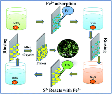
A room temperature successive ionic layer adsorption and reaction (SILAR) method was used to synthesize the FeS thin film in its nanoflakes form onto a 305 grade flexible stainless steel (FSS) substrate as follows: a first beaker containing a 0.05 M FeSO4 aqueous solution was used as the source of the cationic precursor. When the mirror polished FSS substrate was immersed in the cationic solution, the Fe2+ ions are adsorbed on substrate surface via attractive forces such as chemical, van der Waals or other cohesive forces. The loosely bound and excess adsorbed Fe2+ ions were removed using a rinsing process with double distilled water (DDW) in a second beaker. A third beaker containing a 0.02 M Na2S solution was used as the source of S2− ions. The reaction takes place when the pre-adsorbed Fe2+ ions containing FSS substrate was immersed into the anionic precursor solution, resulting in the formation of the FeS thin film. FeS formation can be depicted by the following reaction,| Fe2+ + S2− → FeS | (1) |
Again, as the last step, DDW was used to remove some of the unbound and unreacted species in a second rinsing process. This forms the nucleation centres on the substrate surface. 40 SILAR cycles were repeated to achieve a terminal thickness of the FeS thin film. A schematic illustration of the FeS flakes surface architecture synthesis is depicted in Fig. 1.
Characterization
The crystalline structure and surface morphology of the thin films were examined using X-ray diffraction (XRD, Bruker AXS D8, λ = 1.54 Å), field-emission scanning electron microscopy (FE-SEM, JEOL JSM 6390), transmission electron microscopy (TEM) and high resolution TEM (JEOL JEM 2100). X-ray photoelectron spectroscopy (XPS), VG Multilab 2000, Thermo VG Scientific, UK was used to confirm the binding energies. To confirm the phase of FeS; Raman spectroscopy was performed using a Jobin Yvon Horibra LABRAM-HR visible spectrometer with an argon ion continuous wave laser (532 nm) used as the excitation source. The electrochemical properties were obtained using a Potentiostat/Galvanostat (Princeton Applied Research USA, PARSTAT-4000) with an electrochemical cell in a both two and three electrode assemblies. Based on the current/potential relationships, the electrochemical parameters were calculated (ESI S1†).Results and discussion
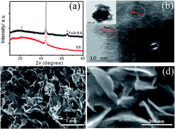
To understand the structural properties, the FeS thin film was characterized using X-ray diffraction (XRD) and is shown in Fig. 2a. The amorphous nature of the FeS thin film was confirmed due to non-existence of any prominent peaks, similar to an earlier report by Manikandan et al.10 In supercapacitor, nanostructured surface morphology provides more ion intercalation or deintercalation at the electrochemically active sites that can enhance the performance during the electrochemical reactions.11,12 In order to further confirm the structure of the FeS thin film, TEM analysis was performed. A cluster of very thin and transparent nanoflakes was observed in the TEM image with the typical size of 10 to 15 nm, which are illustrated in the inset of Fig. 2b. Fig. 2b shows the HR-TEM image of the FeS sample where the lattice fringes with an interplanar spacing of 0.647 nm and 0.289 nm were clearly observed, which corresponds to the (001) and (211) planes, respectively, exhibiting the monoclinic structure of FeS (JCPDS-89-6269). The SAED pattern of the FeS sample displays many concentric blurred diffraction rings representing the amorphous/nanocrystalline nature of the prepared FeS thin film (inset of Fig. 2b).13The surface morphology of the FeS thin film on FSS is shown at two different magnifications in Fig. 2c and d. The SEM image clearly reveals the formation of porous 3-D clustered nanoflakes, which allows easy access for electrolyte ions that helps to reduce the diffusion resistance.14 We believe that, the formation of the flake-like morphology instead of forming a uniform monolayer coating may be due to the following assumptions: (i) the formed layer may not be uniform leading some pinholes on the substrate surface; upon further increasing the number of SILAR cycles, the already formed particles act as nucleation centres for secondary growth leading to formation of a network-like structure, which results in the flake-like morphology, or (ii) the adsorption of small amount of hydroxide content during first step may occur, which results in the formation of iron hydroxide. During the reaction with the S2− ions, the hydroxyl ions are replaced with the sulfur ions to form FeS because the solubility product (Ksp) of Fe(OH)2 (4.87 × 10⁻¹⁷) is greater than FeS (Ksp = 8 × 10⁻¹⁹), this results in a non-uniform coverage, which acts as a nucleation centre for secondary growth; this may be the basis for the flake-like surface architecture. A similar type of surface architecture has been reported for BiOI by Gong et al.;15 whereas, Kulkarni et al. have synthesized β-Ni(OH)2 nanoflakes via the same SILAR method.16
The chemical state of the freshly synthesized FeS thin film was confirmed using X-ray photoelectron spectroscopy (XPS). According to the standard results from the reviewed data, Fe 2p3/2 and Fe 2p1/2 show prominent peaks at 711.5 and 724.7 eV individually in case of only FeS material.17,18 The existence of S2− can be obviously confirmed by the peak at 164.0 eV.19
Fig. 3 shows the complete XPS spectra for the FeS film where the binding energy peaks were centred at 56, 95, 163, 228, 286, 531 eV corresponding to Fe 3p, Fe 3s, S 2p, S 2s, C 1s and O 1s, respectively. The peaks centred at 891, 835 and 780 eV were attributed to the Fe LMM, respectively.20 Additionally, Fig. 3b and c show the high resolution spectra of the Fe and S orbitals, where Fig. 3b depicts the high intensity peaks at 711.3 and 724.2 eV corresponding to Fe 2p3/2 and Fe 2p1/2, respectively.17,18 From Fig. 3c, the peak at 164.11 eV shows the presence of the S2− chemical state and an additional peak at 168.46 eV, which was attributed to sulfur oxygen bonding, possibly due to the sulfate source of Fe or due to air contact.19 The results shows the amorphous phase of FeS, which agrees well with the structural analysis.21,22
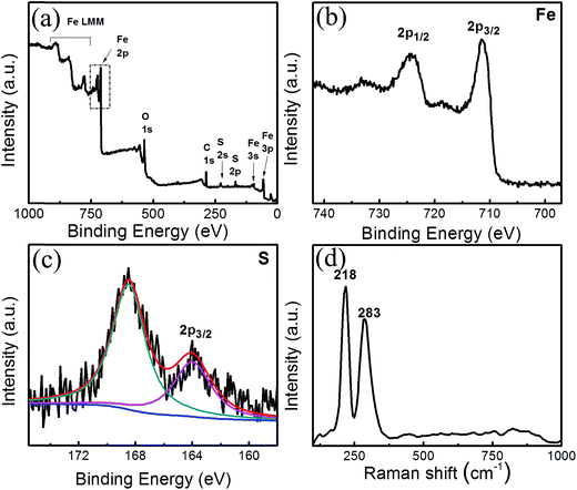 | ||
| Fig. 3 (a) The XPS survey spectra of the FeS sample, (b) the core level Fe 2p spectrum, (c) the core level S 2p spectrum and (d) Raman spectra of the FeS sample. | ||
As the chemically film formation is spontaneous, there may be the probability of the formation of FeS2, Fe3S4 along with FeS. Wang et al.23 have confirmed the formation of FeS2 with the phases at 162.6 and 163.7 eV for S 2p3/2 and S 2p1/2, respectively, which were clearly bonded with Fe 2p1/2 and 2p3/2 at 720.1 and 707.2 eV, respectively. Further, Cao et al.24 reported flower-like microspheres where the Fe 2p3/2 and 2p1/2 orbitals were found at 708.4 and 721.5 eV, which were coupled with the 2p orbitals of S at 161.2 eV, confirming the formation of Fe3S4. From the above literature reports, it was confirmed that there was no chance of forming FeS2 and Fe3S4 in our obtained film. Hence, we conclude that the phase of S, which is coupled with Fe was due to the formation of Fe–S bonding only.
Besides this, the Fig. 3d shows the Raman spectra where two significant peaks were found at 218 and 283 cm−1, which specifies the asymmetric and symmetric stretching modes of FeS.25
The electrochemical behavior of the FeS thin film single electrode
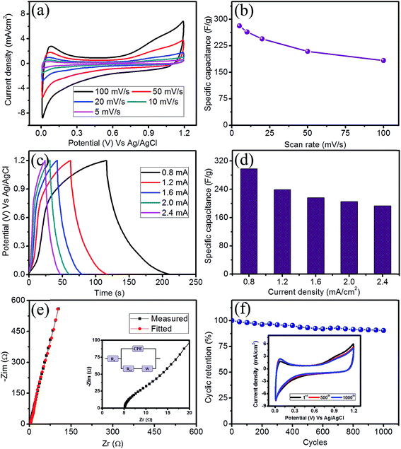
All the electrochemical measurements were employed using a three electrode configuration in which the SILAR prepared FeS thin film acts as the working electrode, a platinum wire acts as the counter electrode and Ag/AgCl acts as the reference electrode. In order to evaluate a suitable electrolyte for the improved performance of the FeS electrode, the electrochemical performance was tested using cyclic voltammetry (CV) in various electrolytes at a concentration of 1 M at fixed scan rate of 100 mV s−1 (ESI S2 (Fig. S2a†)). When comparing all the electrolytes studies, the 1 M LiClO4 electrolyte exhibits not only a high current distribution but also shows the maximum potential window. The obtained specific capacitance of the FeS thin film electrode was 183 F g−1 in LiClO4 and was higher than the other electrolytes studied (Fig. S2b†). Hence, the 1 M LiClO4 electrolyte was used for our electrochemical investigations. The CV curves at different scan rates (5 to 100 mV s−1) are illustrated in Fig. 4a. The closely symmetric rectangular CV shapes along with increasing current distribution with respect to the scan rate implies capacitive behavior. Fig. 4b shows the variation of the specific capacitance with respect to the scan rate. A maximum specific capacitance of 281 F g−1 was obtained at a scan rate of 5 mV s−1. A decreasing specific capacitance was observed with an increasing scan rate due to the occurrence of the complete diffusion of electrolyte ions at a lower scan rate resulting in higher charge storage.The electrochemical performance of an electrode material is evaluated using galvanostatic charge–discharge (GCD) measurements. Fig. 4c shows the GCD curves obtained for the FeS thin film under different galvanostatic conditions ranging from 0.8 to 2.4 mA cm−2 within a fixed potential of 1.2 V. The nearly symmetric triangular shape of the GCD curves indicates capacitive behavior. The sustainability of the GCD curves even at a current density of 2.4 mA cm−2 reveals the high rate capability of the FeS thin film electrode. The values of the specific capacitance were evaluated from GCD curves and are depicted in Fig. 4d. A maximum specific capacitance of 297 F g−1 was observed at a current density of 0.8 mA cm−2, whereas, a specific capacitance of 193 F g−1 was sustained even after a current density of 2.4 mA cm−2. The obtained values supports well with those values obtained through the CV studies.
The resistive behavior of the electrode was inspected using electrochemical impedance spectroscopy (EIS). Fig. 4e shows the EIS spectra of the FeS thin film electrode in the form of Nyquist plot in 1 M LiClO4 electrolyte at an open circuit potential. The initial non-zero intercept followed by a raised arc in the high frequency region on the real axis indicates the solution resistance (Rs) and charge transfer resistance (Rct), respectively. The Rs and Rct for the FeS thin film electrode were found to be 5.15 Ω cm−2 and 7.35 Ω cm−2, respectively. The inset of Fig. 4e shows the equivalent circuit model consists of Rs, the solution resistance; Rct, the charge transfer resistance and W, the Warburg impedance, which arises due to diffusion of the electrolyte ions into the electrode and the constant phase element (CPE), which is due to the semi-infinite diffusion of the electrolyte ions.26,27 The long-term cyclic stability of an electrode is a key factor for the development of a supercapacitor device. Fig. 4f shows the cyclic retention plot of the FeS thin film electrode in 1 M LiClO4 electrolyte at a fixed scan rate of 100 mV s−1 for 1000 cycles. Interestingly, the FeS thin film electrode exhibits 90% retention after 1000 CV cycles. The inset of Fig. 4f shows the CV curves obtained for different cycles at a scan rate of 100 mV s−1 and reveals the insignificant change in the CV shape, confirming less material underwent degradation, even after 1000 CV cycles.
Fabrication of a flexible solid-state symmetric supercapacitor (FSC) device
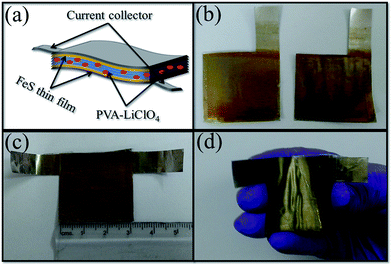
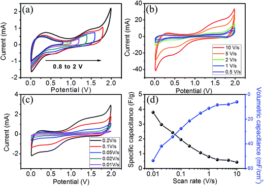
Recently, polymer gel electrolytes have been used for the fabrication of solid-state supercapacitor devices. A FSC device was fabricated using two FeS thin films as the active electrodes sandwiched with a PVA–LiClO4 gel electrolyte,11 which is presented in Fig. 5a–d. The gel electrolyte serves the dual purpose as a separator as well as a solid-state electrolyte in the symmetric device. To assemble the device, one side of each electrode (Fig. 5b) was painted with the gel electrolyte and partially dried at room temperature for 12 h to remove the water content. The edges of both electrodes were masked with tixo-tape to avoid a short circuit in the device (Fig. 5c). Further, these two electrodes with a very thin layer of polymer gel electrolyte were pressed facing the sample area towards each other and normal to the plane of the substrate surface whilst applying a pressure of 1 ton for 10 min to ensure good adhesion along with good mechanical strength for the flexible approach (Fig. 5d). The intention behind constructing the FeS FSC device was to check the practical applicability of the FeS thin film towards portable/flexible device applications.The cyclic voltammetry (CV) curves were obtained for the FeS FSC device by setting 0 V as the initial valve with 0.8 to 2 V as end point at a scan rate of 100 mV s−1 (Fig. 6a) to choose the best suited operational potential window for the formed device, which is a prerequisite to enhance the energy and power density. The formed device exhibits an optimal operational window of 0 to 2 V, which was kept as a base line for performing our further electrochemical studies. Different scan rates (10 to 10![[thin space (1/6-em)]](https://www.rsc.org/images/entities/char_2009.gif) 000 mV s−1) were used to record the CV curves for the formed device where an increase in the current was observed with respect to the increase in the scan rate, which indicates the ideal capacitive behavior of the FeS FSC device (Fig. 6b and c). Furthermore, the CV curves exhibit a partial rectangular shape with a pair of weak redox peaks, which were attributed to the reversible intercalation/deintercalation reaction between Fe2+ and Fe3+ ions in the presence of the Li+ species in the electrolyte as follows,
000 mV s−1) were used to record the CV curves for the formed device where an increase in the current was observed with respect to the increase in the scan rate, which indicates the ideal capacitive behavior of the FeS FSC device (Fig. 6b and c). Furthermore, the CV curves exhibit a partial rectangular shape with a pair of weak redox peaks, which were attributed to the reversible intercalation/deintercalation reaction between Fe2+ and Fe3+ ions in the presence of the Li+ species in the electrolyte as follows,
| FeS + xLi+ + xe− ↔ LixFeS | (2) |
The network-like structure of the PVA–LiClO4 gel with the lower ionic radius of Li+ ions (0.076 nm) was feasible for the large charge transfer of ions during the electrochemical charge storage process.8 The values obtained for the specific and volumetric capacitance of the device at different scan rates are presented in Fig. 6d. The value of the capacitance (specific and volumetric) decreased with an increase in the scan rate, which was attributed to the lower utilization of electroactive sites in the material by the electrolyte ions based on the time constraints. In other words, only the outer active surface is utilised at a high scan rate while at a lower scan rate, the electrolyte ions have enough time to utilize all the active sites of electrodes during the charge storage process.28 Even at a very high scan rate, the shape of the CVs do not change demonstrating the excellent reversibility and high power response properties of the electrode material. At a scan rate of 10 mV s−1, remarkable specific and volumetric capacitances were achieved as 3.79 F g−1 and 53.53 mF cm−3, respectively.
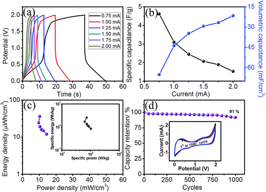
In order to evaluate the actual working potential of the supercapacitor device, the symmetric FSC device was studied using GCD measurements over different potential windows (ESI S3†). Also, to evaluate the values of the energy and power densities, GCD studies were performed. Deviation from the linear variation of the GCD curves at various galvanostatic current values demonstrated the faradic capacitive characteristics,29 as shown in Fig. 7a. The maximum specific and volumetric capacitance values obtained from the GCD curves are 4.62 F g−1 and 65.17 mF cm−3, respectively at a galvanostatic current of 0.75 mA (Fig. 7b). Significantly, 33% retention in the capacitance value was observed even after a constant current of 2 mA. The decreasing capacitance with an increasing galvanostatic current was attributed to the significant formation of a barrier against penetration and diffusion of Li+ ion species in the electrolyte.28 For the symmetric supercapacitor device, a Ragone plot (Fig. 7c) showed the maximum values of specific energy and specific power obtained at a current of 0.75 mA as 2.56 W h kg−1 (36.11 μW h cm−3) and 726 W kg−1 (10.24 mW cm−3), respectively. It is observed that the specific energy was maintained at 0.85 W h kg−1 (11.98 μW h cm−3) with a specific power of 1018 W kg−1 (14.37 mW cm−3) even after a constant current of 2 mA, which reveals that the increase in specific current results in a decrease in the specific energy with an upsurge in the specific power. Thus, even at a very high current density, our device exhibits better power retention without a significant loss in the energy density. In order to check the cyclic stability of the device, a CV cycling test was performed for 1000 cycles at a scan rate of 100 mV s−1 within the same potential window from 0 to 2 V and depicted in the inset of Fig. 7d, which shows an insignificant change (9%) and 91% retention (Fig. 7d) after 1000 cycles, implying the stable nature of the device.
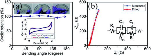
The size of the device can be tuned with the aid of an axial type supercapacitor device for portable electronic application, which is a requisite for highly flexible electrodes. To explore this, bending of the device was performed up to 175° with steps of 30° using CV measurements at each step at a scan rate of 100 mV s−1 (Fig. 8a). The excellent stability during bending even though a flexible approach with mechanical bending could produce stress along the elongated direction limits its charge storage behavior.30 Interestingly, our device overcome this issue and exhibits no change in the CV profile by retaining a cyclic performance of 100% even at a bending angle of 175°.
Electrochemical impedance spectroscopy (EIS) was performed in the frequency range of 0.1 Hz to 10 kHz and is shown in Fig. 8b. An Nyquist plot and ZSimpWin software simulation method based on the equivalent circuit were used to analyse the EIS spectra, as shown in the inset of Fig. 8b. A nearly vertical line in the Nyquist plot presents the ideal supercapacitor behavior whereas the occurrence of a small arc in the high frequency region was a result of the interfacial charge transfer resistance.31 The internal resistance (Rs) of the active electrode can be estimated using the intersecting point obtained on the real axis in the high frequency region along with ionic resistance, the inherent resistance of the material and the contact resistance of electrode material and electrolyte.32 Our prepared device shows an Rs value of 11.6 Ω whereas a charge transfer resistance (Rct) of 8.3 Ω between the electrode and electrolyte was obtained from diameter of the arc. The small arc exhibits good electrical conductivity with a low value for the material resistance.31 The nearly parallel straight line to the imaginary axis shows an ideal polarizable capacitance (CL) at low frequency.33 The plot tending at an angle to the real axis demonstrates the association of resistance with CL, which was designated as the leakage resistance (RL) and was linked parallel to the CL. The evolution from high frequency arc to the low-frequency tail was embedded by the Warburg element (W).34
The commercial feasibility can be checked by demonstrating the device towards its practical application. To raise this illustration, the device was charged for 10 s by applying a constant voltage and discharged through a panel consisting of 21 red LEDs. Impressively, this symmetric FSC device can easily light up the system of LEDs (Fig. 9a). Correspondingly, Fig. 9b–e shows the images of the decreasing light intensity of one red LED during discharging up to 30 s, which clearly demonstrating the great potential of the device (ESI video†).
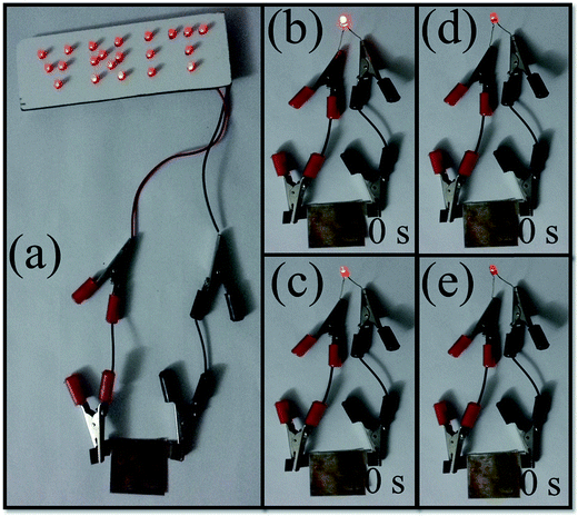 | ||
| Fig. 9 (a) A practical demonstration of the FeS FSC device by lighting 21 red LEDs. (b–e) A practical demonstration of the FeS symmetric FSC device lighting an LED with respect to time (0 s to 30 s). | ||
Conclusions
A unique approach to construct a FeS based flexible solid-state symmetric supercapacitor (FSC) device with an impressive operational potential window of 2 V has been successfully demonstrated. The use of a simple, cost-effective and facile SILAR method at room temperature (27 °C) was explored and its applicability to form a FeS supercapacitor active electrode was demonstrated. The as-prepared FSC device gained a capacitance of 4.62 F g−1 (65.17 mF cm−3) at a galvanostatic current of 0.75 mA along with a high specific energy of 2.56 W h kg−1 (36.11 μW h cm−3). The symmetric device exhibits excellent cyclic stability with a 91% retention of the initial value over 1000 cycles along with bending the device up to 175°, which clearly shows its possible use in bendable portable electronics. Furthermore the solid-state device has lit a 21 red LEDs panel demonstrated its potential applicability.Acknowledgements
The authors are thankful to the DST-SERB, India (Do. No. SB/S2/CMP/032/2013; 4/06/2013) and STIC, Cochin University, Cochin. P. D. thanks Director V.N.I.T. for financial assistance of the M. Sc. project.References
- N. A. Kyeremateng, T. Brousse and D. Pech, Microsupercapacitors as miniaturized energy-storage components for on-chip electronics, Nat. Nanotechnol., 2017, 12, 7 CrossRef CAS PubMed.
- D. P. Dubal, N. R. Chodankar, Z. Caban-Huertas, F. Wolfart, M. Vidotti, R. Holze, C. D. Lokhande and P. Gomez-Romero, Synthetic approach from polypyrrole nanotubes to nitrogen doped pyrolyzed carbon nanotubes for asymmetric supercapacitors, J. Power Sources, 2016, 308, 158 CrossRef CAS.
- C. H. Lai, M. Y. Lu and L. J. Chen, Metal sulfide nanostructures: synthesis, properties and applications in energy conversion and storage, J. Mater. Chem., 2012, 22, 19 RSC.
- A. M. Patil, A. C. Lokhande, N. R. Chodankar, V. S. Kumbhar and C. D. Lokhande, Engineered morphologies of β-NiS thin films via anionic exchange process and their supercapacitive performance, Mater. Des., 2016, 97, 407 CrossRef CAS.
- D. J. Vaughan, U. Becker and K. Wright, Sulphide mineral surfaces: theory and experiment, Int. J. Miner. Process., 1997, 51, 1 CrossRef CAS.
- N. R. Chodankar, D. P. Dubal, G. S. Gund and C. D. Lokhande, A symmetric MnO2/MnO2 flexible solid state supercapacitor operating at 1.6 V with aqueous gel electrolyte, J. Energy Chem., 2016, 25, 463 CrossRef.
- Q. Wang, X. Wang, B. Liu, G. Yu, X. Hou, D. Chen and G. Shen, NiCo2O4 nanowires arrays supported on Ni foam for high-performance flexible all-solid-state supercapacitors, J. Mater. Chem. A, 2013, 1, 2468 CAS.
- A. M. Patil, A. C. Lokhande, N. R. Chodankar, P. A. Shinde, J. H. Kim and C. D. Lokhande, Interior design engineering of CuS architecture alteration with rise in reaction bath temperature for high performance symmetric flexible solid state supercapacitor, J. Ind. Eng. Chem., 2017, 46, 91 CrossRef CAS.
- R. B. Pujari, A. C. Lokhande, A. A. Yadav, J. H. Kim and C. D. Lokhande, Synthesis of MnS microfibers for high performance flexible supercapacitors, Mater. Des., 2016, 108, 510 CrossRef CAS.
- K. Manikandan, P. Mani, C. Surendra Dilip, S. Valli, P. Fermi Hilbert Inbaraj and J. Joseph Prince, Effect of complexing agent TEA: the structural, morphological, topographical and optical properties of FexSx nano thin films deposited by SILAR technique, Appl. Surf. Sci., 2014, 288, 76 CrossRef CAS.
- N. R. Chodankar, D. P. Dubal, G. S. Gund and C. D. Lokhande, Bendable All-Solid-State Asymmetric Supercapacitors based on MnO2 and Fe2O3 Thin Films, Energy Technol., 2015, 3, 625 CrossRef CAS.
- D. P. Dubal, P. Gomez-Romero, B. R. Sankapal and R. Holze, Nickel cobaltite as an emerging material for supercapacitors: an overview, Nano Energy, 2015, 11, 377 CrossRef CAS.
- S. S. Raut and B. R. Sankapal, First report on synthesis of ZnFe2O4 thin film using successive ionic layer adsorption and reaction: approach towards solid-state symmetric supercapacitor device, Electrochim. Acta, 2016, 198, 203 CrossRef CAS.
- P. R. Jothi, R. R. Salunkhe, M. Pramanik, S. Kannan and Y. Yamauchi, Surfactant-assisted synthesis of nanoporous nickel sulfide flakes and their hybridization with reduced graphene oxides for supercapacitor applications, RSC Adv., 2016, 6, 21246 RSC.
- J. Gong, X. Wang, X. Li and K. Wang, Highly sensitive visible light activated photoelectrochemical biosensing of organophosphate pesticide using biofunctional crossed bismuth oxyiodide flake arrays, Biosens. Bioelectron., 2012, 38, 43 CrossRef CAS PubMed.
- S. B. Kulkarni, V. S. Jamadade, D. S. Dhawale and C. D. Lokhande, Synthesis and characterization of β-Ni(OH)2 up grown nanoflakes by SILAR method, Appl. Surf. Sci., 2009, 255, 8390 CrossRef CAS.
- A. R. Pratt, I. J. Muir and H. W. Nesbitt, X-ray photoelectron and Auger electron spectroscopic studies of Pyrrhotite and mechanism of air oxidation, Geochim. Cosmochim. Acta, 1994, 58, 827 CrossRef CAS.
- J. E. Thomas, W. M. Skinner and R. S. t. C. Smart, A comparison of the dissolution behavior of troilite with other iron(II) sulfides; implications of structure, Geochim. Cosmochim. Acta, 2003, 67, 831 CrossRef CAS.
- H. Geng, L. Zhu, W. Li, H. Liu, L. Quan, F. Xi and X. Su, FeS/nickel foam as stable and efficient counter electrode material for quantum dot sensitized solar cells, J. Power Sources, 2015, 281, 204 CrossRef CAS.
- P. S. Shinde, A. Annamalai, J. H. Kim, S. H. Choi, J. S. Lee and J. S. Jang, Photoelectrochemical, impedance and optical data for self Sn-diffusion doped Fe2O3 photoanodes fabricated at high temperature by one and two step annealing method, Data Brief., 2015, 5, 796 CrossRef PubMed.
- G. Genchev and A. Erbe, Raman spectroscopy of Mackinawite FeS in Anodic Iron sulfide Product, J. Electrochem. Soc., 2016, 163, C333 CrossRef CAS.
- A. R. Lennie, S. A. T. Redfern, P. E. Champness, C. P. Stoddart, P. F. Schofield and D. J. Vaughan, Transformation of Mackinawite to greigite; an in situ X-ray powder diffraction and transmission electron microscope study, Am. Mineral., 1997, 82, 302 CAS.
- M. Wang, C. Xing, K. Cao, L. Zhang, J. Liu and L. Meng, Template-directed synthesis of pyrite (FeS2) nanorods arrays with an enhanced photoresponse, J. Mater. Chem. A, 2014, 2, 9496 CAS.
- F. Cao, W. Hu, L. Zhou, W. Shi, S. Song, Y. Lei, S. Wang and H. Zhang, 3D Fe3S4 flower-like microspheres: high-yield synthesis via a biomolecule-assisted solution approach, their electrical, magnetic and electrochemical hydrogen storage properties, Dalton Trans., 2009, 42, 9246 RSC.
- A. Boughriet, R. Figueiredo, J. Laureyns and P. Recourt, Identification of newly generated iron phases in recent anoxic sediments: 57Fe Mossbauer and microRaman spectroscopic studies, J. Chem. Soc., Faraday Trans., 1997, 93, 3209 RSC.
- D. P. Dubal, G. S. Gund, C. D. Lokhande and R. Holze, Decoration of spongelike Ni(OH)2 nanoparticles onto MWCNTs using an easily manipulated chemical protocol for supercapacitors, ACS Appl. Mater. Interfaces, 2013, 5, 2446 CAS.
- B. Pandit, D. P. Dubal, P. Gomez-Romero, B. B. Kale and B. R. Sankapal, V2O5 encapsulated MWCNTs in 2D surface architecture: complete solid-state bendable highly stabilized energy efficient supercapacitor device, Sci. Rep., 2017, 7, 43430 CrossRef PubMed.
- V. Augustyn, P. Simon and B. Dunn, Pseudocapacitive oxide materials for high-rate electrochemical energy storage, Energy Environ. Sci., 2014, 7, 1597 CAS.
- D. P. Dubal, G. S. Gund, R. Holze, H. S. Jadhav, C. D. Lokhande and C. J. Park, Solution-based binder-free synthetic approach of RuO2 thin films for all solid state supercapacitors, Electrochim. Acta, 2013, 103, 103 CrossRef CAS.
- D. P. Dubal, J. G. Kim, Y. Kim, R. Holze, C. D. Lokhande and W. B. Kim, Supercapacitors based on flexible substrates: an overview, Energy Technol., 2014, 2, 325 CrossRef.
- C. C. Hu, K. H. Chang and T. Y. Hsu, The synergistic influence of OH− Concentration and Electrolyte Conductivity on the redox behavior of Ni(OH)2/NiOOH Physical and Analytical electrochemistry, J. Electrochem. Soc., 2008, 155, F196 CrossRef CAS.
- P. Yang and W. Mai, Flexible solid-state electrochemical supercapacitors, Nano Energy, 2014, 8, 274 CrossRef CAS.
- C. Masarapu, H. F. Zheng, K. H. Hung and B. Wei, Effect of Temperature on the Capacitance of Carbon Nanotube Supercapacitors, ACS Nano, 2009, 3, 2199 CrossRef CAS PubMed.
- B. Saravanakumar, K. K. Purushothaman and G. Muralidharan, Interconnected V2O5 Nanoporous Network for High-Performance Supercapacitors, ACS Appl. Mater. Interfaces, 2012, 4, 4484 CAS.
Footnote |
| † Electronic supplementary information (ESI) available. See DOI: 10.1039/c7se00165g |
| This journal is © The Royal Society of Chemistry 2017 |

