Extrusion of a nano-ordered active layer for organic photovoltaic cells
Ali
Nourdine
 *ab,
Lionel
Flandin
ab,
Nicole
Albérola
ab,
Lara
Perrin
ab,
Emilie
Planès
ab,
Anne
Hiltner
cd and
Eric
Baer
cd
aUniversité Savoie Mont-Blanc, LEPMI, F-73000 Chambéry, France. E-mail: ali.nourdine@univ-savoie.fr
bCNRS, LEPMI, F-38000 Grenoble, France
cCenter for Layered Polymeric Systems, Case Western Reserve University, Cleveland, OH 44106-7202, USA
dDepartment of Macromolecular Science and Engineering, Case Western Reserve University, Cleveland, OH 44106-7202, USA
First published on 27th September 2017
Abstract
For the first time, an extrusion process is used to produce a perfectly nanostructured organic photoactive layer. Extrusion is an interesting, inexpensive and environment-friendly (solventless) option allowing an industrial production scale for polymer solar cell technology. In this paper, this plausible alternative to the usual large scale wet-processing techniques (inkjet printing, roll-to-roll coating…) was considered in order to elaborate bulk lamellar ordered heterojunctions employing polythiophene and fullerene based materials, as the electron donor and acceptor respectively, which were specifically elaborated for this work. An alternating donor/acceptor (D/A) lamellar structure close to the ideal interpenetrating system was targeted and successfully realized. Continuous D and A domains of about 24 nm were obtained, i.e. size close to the exciton diffusion length (20 nm) for π-conjugated organic materials; a photovoltaic response was evidenced under AM1.5 light simulator conditions. This photovoltaic effect, observed in spite of the presence of insulating polymers (∼61 wt%) added in both semi-conductor materials in order to adjust their viscosities, proves the possible achievement of such a perfect working nano-architectured structure via the extrusion process. The next step, consisting in the use of pure D and A extrudable polymers, should thus lead to high and durable photovoltaic performances. Therefore, this paper opens the way to a new promising OPV processing method: extrusion.
1. Introduction
First described in the 1970s, organic photovoltaic (OPV) technology has remarkable advantages such as low-cost, low-weight, flexibility and large-size processability. However, in order to make it a real alternative to inorganic technology, several challenges must be overcome by controlling the nanoscale morphology of the active layer1–5 and by including the development of processes compatible with large-scale production.6,7 In addition to the intrinsic properties of the donor and acceptor materials,4 the morphology of the active layer is a crucial parameter that controls the power conversion efficiency. The photovoltaic effect and the charge photogeneration in organic photovoltaic solar cells occur at the interfaces between the D and A materials. Thus, increasing the amount of D/A interface improves the photovoltaic efficiencies.8,9 This also implies a size reduction of D and A domains, which should be carefully kept lower than the exciton diffusion length (10–20 nm).4,8,10 Traditionally, morphology improvement can be realized during or after the active layer wet-deposition through several ways: – modification of the D/A ratio,11,12 – change of the solvent,13 – use of processing additives,14–16 – vapor17,18 or – thermal13,19,20 annealing treatments. Other new methods are also constantly developed in order to directly obtain an effective morphology. We can cite, in particular, the discontinuous stacking of several nanolayers of D and A materials by spin-coating,5 the alignment by soft lithography techniques,4 the genesis of lamellar structures using self-assembly materials,20–25 polymer demixing,26 nanoimprinting,27–30 nanoskiving,5 controlled organic vapor-phase deposition31 and photoinduced mass transport using an all-optical technique.32 These efficient methods yielded interesting new hetero-structures that satisfy some of the criteria required for an ordered bulk heterojunction but they imply the use of organic solvents and are limited to lab-scale production. For a large-scale production, the ideal process should involve processing of all layers on flexible substrates by the combination of as few coating and printing steps as possible. The process should be free from the costly indium, solvents and toxic chemicals and the final polymer solar cell product should have a low environmental impact and a high degree of recyclability. The conventional way to fabricate a flexible organic solar cell is roll to roll coating, but it presents the main drawback, the use of solvents.6,20 In the present paper, the groundbreaking concept proposed consists in the realization of an ideal nanoscale lamellar morphology by alternatively layering D and A polymeric materials via the “coextrusion forced assembly technique”. This process will open a new direction for future low-cost plastic electronic devices and can contribute to the efforts and research advances carried out in the development of clean energy-generating photovoltaic technologies such as green-solvent-processable OPVs33–35 and can be considered as a plausible solventless and environment-friendly processing alternative compared to the usual wet-processing techniques, using, for instance, printing6,36–38 or roll-to-roll coating6,39–41 and, especially, halogenated solvents.This “forced assembly technique”, which has been developed by the Center for Layered Polymeric Systems (CLiPS) at Case Western Reserve University, allows for the layering of two polymers using layer multiplication coextrusion techniques.42–49 This original process has been used for structuring usual polymers, and the thickness of these layers has reached nanometer sizes, allowing for unique optical, mechanical, transport, and structural properties.42–49
With this ideal architecture applied to a photo-active layer, the photovoltaic devices should thus lead to high and stable photovoltaic efficiencies. Nevertheless, in order to maximize the uniformity of the layers and overall D/A heterojunction quality, D and A polymeric materials must be coextruded at a viscosity-match temperature50–52 and within a viscosity window determined by the extrusion pressure (upper limit of 0.1 MPa s) and the melt strength (lower limit of 0.01 MPa s).50 Indeed, two main defects related to the difference of rheological behaviors and viscoelastic characteristics of polymers can be observed: layer-to-layer non-uniformity of thickness52–57 and discontinuity of the phase due to interfacial instability.51,52,56,57 Accordingly, to study the feasibility of co-extrusion as a new concept for production of OPV layers, the principal criteria which we first considered in the present work is the processing ability of D and A materials, keeping in mind that their intrinsic functional properties could be adjusted subsequently in order to optimize performances.
Thus, the first part of the paper will describe D and A materials specifically formulated for the preparation of extrudable solar cells, taking into account several needed criteria – firstly – for the special processing conditions and – secondly – for the photovoltaic properties. Then, the fabrication of “multi-nanolayer” photo-active films using the forced assembly coextrusion process and the final realization of “D/A nanolayer solar cells” will be both expounded.
2. Results and discussion
2.1. Choice of D and A materials: selection and adjustment
The polythiophene/fullerene conventional donor/acceptor system was selected in order to realize the first OPV active layer by extrusion. The polythiophene family was chosen because of its interesting photovoltaic properties and compatibility with processing in a molten state.58–64 The regioregular poly(3-octylthiophene) P3OT was thus selected, as it exhibits a good compromise between photovoltaic properties and extrusion conditions compared to the other poly(3-alkylthiopene) derivatives.65,66 Furthermore, its commercial availability in large amounts makes it an obvious candidate. As a matter of fact, one co-extrusion test requires about 100 g. Regarding the fullerene derivative, it was chosen to synthesize a polystyrene grafted using fullerene C60. Indeed, intrinsic acceptor polymers reported in literature are mostly unprocessable from the melt, because they degrade at temperatures below the softening temperature.67–69 The use of a common polymer easy to be processed – like polystyrene (PS) – grafted using an efficient acceptor – like C60 fullerene – could thus be an interesting alternative. According to the electrical percolation threshold (Vc = 4 vol%) evidenced in our previous studies70,71 for such PS-grafted-C60 systems, an acceptor polymer was specifically synthesized in large quantity (∼100 g): PSNC60MS12 (containing 12 vol% of C60, corresponding to 19 wt%).| Materials | Fusion | Crystallization | Crystallinity degree X (%) | ||||
|---|---|---|---|---|---|---|---|
| T peakm (°C) | T endset (°C) | ΔHf (J g−1) | T peakc (°C) | T onsetc (°C) | ΔHc (J g−1) | ||
| PP | 164 | 169 | 90 | 109 | 113 | −94 | 44 |
| P3OT65/PP35 | 163 | 167 | 31 | 113 | 118 | −28 | 26 |
| P3OT | 184 | 195 | 13 | 146 | 153 | −13 | 18 |
This melt viscosity value is slightly below the range required for our coextrusion process (i.e. [0.01–0.1 MPa s]); an adjustment of the rheological behavior is thus essential. In order to overcome this limitation and modulate the melt viscosity of the donor material, several ways were considered and investigated: decrease of the coextrusion temperature,63 synthesis of P3OT with higher molecular weights,63,64 or use of a blend of commercial miscible polymers.72 First, the P3OT viscosity remains too low even at temperatures close to the melting temperature (0.0085 MPa s at 195 °C). Then, the synthesis way was explored and P3OT with a higher molecular weight was realized (Mw eq.PS = 140 kg mol−1). Unfortunately, one potential problem encountered in processing unsaturated polymers at high temperatures is the occurrence of crosslinking reactions, whose effect is emphasized when working with higher Mw.63 As a result, the newly synthesized P3OT becomes infusible due to cross-linkage at temperatures higher than the melting temperature and thus non-extrudable. Finally, a blend of P3OT with another semi-crystalline polymer having a similar processing temperature and higher viscosity was chosen.
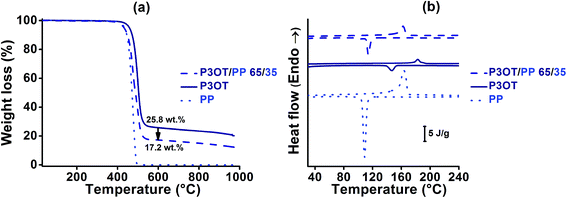
To achieve the latter approach, a semi-crystalline polypropylene PP polymer was chosen as the diluent polymer. The P3OT/PP polymer blends were elaborated using a twin screw extruder at temperatures close to 195 °C. This temperature was chosen above the melting temperature of all constituents (see Table 1), and well below their TGA decomposition temperatures (higher than 300 °C under air, and 400 °C under nitrogen). A viscous P3OT/PP system was obtained; its composition and homogeneity were controlled by TGA and DSC analyses as shown in Fig. 1a and b, respectively.
The real composition of the D material after melt blending by extrusion can be checked using TGA analysis under an inert atmosphere as shown in Fig. 1a. A good agreement was found with the initial composition introduced in the extruder, which indicates the thermal stability of the P3OT/PP system during the extrusion process. A blend composition of 65 wt% and 35 wt% for P3OT and PP respectively, leading to a melt viscosity of 0.15 MPa s at 195 °C, was selected in order to be both inside the compatible process viscosity range and remain close to the viscosity of the acceptor system (see Fig. 3).
A good homogeneity of the system is also important in order to guarantee the success of the coextrusion process. As shown in Fig. 1b and Table 1, DSC analysis highlights the presence of co-crystallization phenomena for semi-crystalline PP and P3OT polymers: one single melting Tm and one single crystallization Tc temperatures were detected for the P3OT/PP 65/35 blend. Co-crystallization results in a homogeneous and miscible system, as also observed by optical microscopic analysis (not presented in this paper).
In order to verify that sufficient conductive properties for OPV application were preserved in the new donor material, electrical properties were measured for both pure and blended polythiophene based materials after one extrusion test. Electrical conductivities close to 1.1 × 10⁻⁶ and 2 × 10⁻⁹ S cm−1 were found for P3OT and P3OT/PP 65/35 respectively. As predicted, the conductive properties of the donor material decrease when an insulating polymer is added in a homogeneous blend with the conjugated polymer.73,74 Nevertheless, an acceptable compromise between the extrusion process and photovoltaic74,75 compatibilities was found using the P3OT/PP 65/35 blend.
When controlling the melt viscosity of PSCN60MS12 using the Melt Flow Index (MFI), an unexpected behaviour was observed. Indeed, if the first melt viscosity value measured is well inside the coextrusion process compatibility range (i.e. [0.01–0.1 MPa s]), this value is not stable and increases drastically by two orders of magnitude after 3 MFI cycles as shown in Fig. 3 (0.015, 0.068 and 0.71 MPa s for cycles 1, 2 and 3, respectively, at a temperature of 200 °C). This behaviour could be explained by possible chemical cross-linking (formation of fullerene–fullerene covalent bonds by ageing) and/or by phase separation resulting in the formation of fullerene aggregates as previously evidenced for higher fullerene contents in our previous work.71 It was thus decided to reduce the fullerene content by adding a small amount of the polystyrene polymer with close viscosity, and it was found that the initial rheological behaviour of the PSNC60MS12/PS blend can be stabilized and maintained constant during the extrusion process. The addition of 30 wt% of PS into PSNC60MS12 enables adjustment of the melt viscosity to 0.02 MPa s at 195 °C, which is both compatible with the process and close to the one of the chosen D material. Moreover, the resulting C60 content (8 vol% or 13 wt%) remains over the percolation threshold. Thus, the semiconductor character and the applicability in photovoltaic solar cells are preserved.
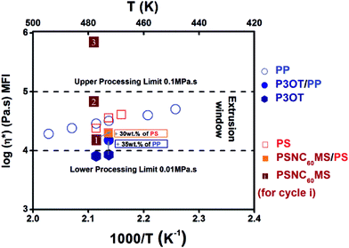 | ||
| Fig. 3 Logarithmic viscosity (Melt Flow Index, MFI) of constitutive polymer materials as a function of temperature. | ||
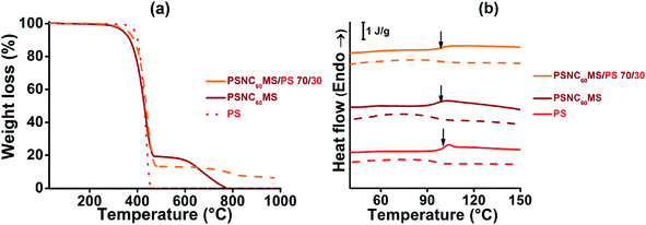
A PSNC60MS12/PS acceptor material with a blend composition of 70 wt% for PSNC60MS12 and 30 wt% for PS was elaborated using a twin screw extruder at the temperature of 195 °C. This temperature is well below the decomposition temperature of the selected A material (close to 300 °C for all constituents, determined by TGA under air). In addition, a TGA analysis performed under nitrogen (see Fig. 2a) on the PSNC60MS12/PS blend after extrusion indicates that the PS/C60 composition remains stable during extrusion (the C60 content being represented by the degradation residue at 550 °C).
Amorphous PS polymer was chosen as the diluent polymer because of its presumed physico-chemical compatibility with PSNC60MS in order to obtain a miscible and homogeneous system which was confirmed by optical microscopy analysis (not presented in this paper). The molecular mobility of macromolecular chains was also studied by DSC analysis of the temperature location of glass transition (Tg), which was found to be independent of the blend composition and approaching 100 ± 1 °C, as shown in Fig. 2b.
A reasonable processing temperature close to 195 °C was chosen. At this temperature, pure P3OT exhibits melt viscosity below the lower limit. The resulting readjusted viscosity by addition of 35 wt% of PP matches the required range of viscosity. In contrast, the melt viscosity of pure PSNC60MS12 at this range of temperature is adequate with the extrusion process but its rheological behaviour is unstable. The addition of 30 wt% of PS allowed a slight modulation of the viscosity while obtaining a stable rheological behaviour.
Another important parameter for success in the realization of the nanolayers using our process is the close rheological behaviour of the two selected materials at the chosen temperature. Indeed, the ratio of their viscosities should not exceed 3. This is fully the case of the selected materials at 195 °C: ηA/ηD = 1.3.
2.2. The photoactive layer realization: A/D multi-layers
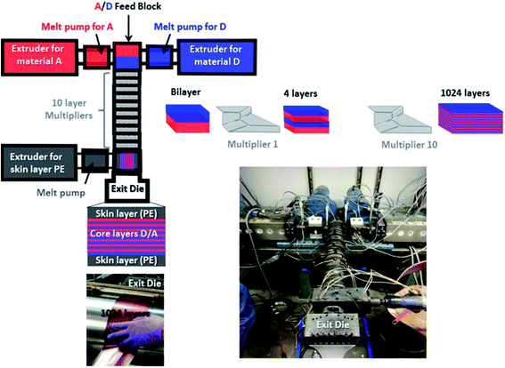 | ||
| Fig. 4 Presentation of the extrusion process used and photographs taken during the fabrication of the nano-multilayer film. | ||
Coextrusion experiments were performed at the Case Western Reserve University on a semi-laboratory scale coextrusion line that incorporates 10 multipliers, allowing the realization of 1024 alternating layers. This extrusion process is fully detailed in the literature42–49 and has already been used to nano-structure several common polymers like PP, PE, PEG, PMMA, PS, PC, SAN, PET, …. The originality and novelty of the present work lie in the use of this process for the elaboration of nano-structured photovoltaic active layers using specifically formulated high performance polymeric materials.
Prior to the real rush, several coextrusion tests were performed using only PS and PP model polymers for realization of the alternating nanolayered system (core layers). PS and PP polymers with specific grades indicated in the experimental section were selected because of their processing properties and microstructures being close to A and D materials respectively. LDPE was also used as the surface layer (skin layer), allowing the manipulation of the film while preserving its integrity. After optimization of the coextrusion conditions, optimal temperatures close to 195 °C for coextrusion of core layers, 190 °C for extrusion of skin layers and 165 °C at the exit die were determined and applied to real D (P3OT/PP 65/35 wt%) and A (PSNC60MS12/PS 70/30 wt%) materials. In order to avoid wasting D and A, which are expensive photoactive materials, previously reported PP and PS polymers were also used as carrier materials in order to both initiate and end the extrusion run.
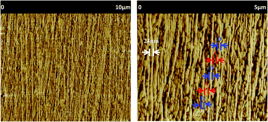
A nanolayered film with 1024 alternating D/A layers was successfully extruded (see the photograph of the film in Fig. 4), and its continuous and uniform layered structure was revealed by atomic force microscopy observation (see the phase image presented in Fig. 5). D/A nanolayers are well-resolved with an average layer thickness of 24 nm, and the total thickness of the obtained film is close to 55 μm (PE 10 μm–multi-D/A 25 μm–PE 10 μm).
![[thin space (1/6-em)]](https://www.rsc.org/images/entities/char_2009.gif) 000 alternating D/A layers (cf.Fig. 6a).
000 alternating D/A layers (cf.Fig. 6a).
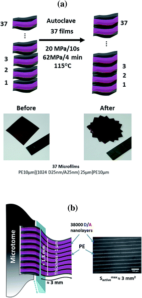 | ||
| Fig. 6 (a) Explanation scheme of the consolidation approach. (b) Representation of the microtome cutting step with the optical micrograph of the consolidated photoactive films. | ||
In order to better preserve the D/A-multilayered structure, the consolidation was performed with the LDPE skin layer. This allows working at rather low temperatures close to the LDPE melting temperature (between 90 and 120 °C). To define the optimal consolidation conditions, preliminary tests using different temperatures, pressures and times were performed beforehand on model multi-layered films (PE 10 μm–PP/PS 25 μm–PE 10 μm), which are very similar in mechanical behavior to the photo-active film (PE 10 μm–multiD/A 25 μm–PE 10 μm). The approach to achieve optimal conditions evidenced consist, in the first step, in consolidating the films at 115 °C under a pressure of 20 MPa for 10 s and then increasing the pressure to 62 MPa for 4 min before letting the consolidated films to cool down to room temperature.
The consolidation quality was evaluated by optical microscopy analysis after microtome cutting (cf.Fig. 6b, the light and dark bands corresponding respectively to the LDPE skin layer and D/A core multi-layers).
2.3. Solar cell realization and characterization
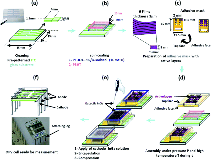
In our configuration, both electrodes should be deposited on the photo-active film, and not the reverse as for usual OPV cells. Thus, in order to develop a specific assembly procedure for “D/A nanolayer solar cells”, it was necessary to test different configurations and conditions including: active layer thickness (0.5 or 1 μm), cathode nature and deposition process (Al using Joule effect evaporation in a vacuum chamber or an InGa eutectic by drop casting), intermediate hole transporting monolayer (pure PEDOT–PSS, doped PEDOT–PSS/PEG or PEDOT–PSS/D-sorbitol with various ratios) or multilayer (PEDOT–PSS/P3OT or PEDOT–PSS/P3HT and PEDOT–PSS/D-sorbitol) with or without annealing (thermal or solvent vapor), lamination at various temperatures (room temperature, or around the melting temperature of D-sorbitol: 70 and 80 °C) under different pressures (0, ≈50 and ≈75 kPa) and for different times (2 and 5 min).A large series of “D/A nanolayer solar cells” (>500 devices) has been tested. In this paper, we report the actual investigation of the optimal conditions, as described in Fig. 7. First, 40 to 50 nm of conducting PEDOT–PSS doped with D-sorbitol was deposited on pre-patterned ITO substrates. This transparent intermediate layer acts as an adhesive conductive layer between the active layer film and the ITO anode, helping during the lamination step and ensuring a good electrical contact between the two parts. An additional very thin layer (≈10 nm) of P3HT was also added, allowing both an improvement of the active/intermediate layer interface and an increase of the hole transport, while not affecting the adhesive properties of PEDOT–PSS/D-sorbitol. Then, an adhesive mask with six patterned “windows” (1 × 2 mm2) was placed. On each window, a “D/A nanolayer film” with thickness = 1 μm and area ≈ 1.8 × 3 mm2 was dropped, and the assembly was realized at 80 °C under a 50 kPa pressure for 5 min. Finally, an InGa metal droplet was deposited as the top cathode and the solar cell was encapsulated by sticking an encapsulation glass.
For electrical characterization, electrical connection legs were then attached (Fig. 7f). And, as shown in Fig. 8, a reproducible photovoltaic result is observed using the “extruded D/A nanolayer film” as the photoactive layer. According to the J–U photovoltaic characteristic curve under AM1.5 illumination, the open-circuit voltage Voc of the device is close to 0.92 V, and the short-circuit current density Jsc is close to 0.016 A m−2. This latter value thus evidences a photoinduced charge transfer within the “D/A nanolayer solar cell”.
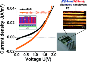 | ||
Fig. 8 Current density–voltage curves of “D/A nanolayer solar cells” under illumination (AM1.5G, 100 mW cm−2) ( ) and dark ( ) and dark ( ). ). | ||
The high Voc (0.92 eV) measured for the “D/A nanolayer solar cell” could be attributed to (i) the solar cell assembly conditions;77 (ii) the effective interface percolated active D/active A ratio;78 (iii) the large number of D/A heterojunctions79 (19![[thin space (1/6-em)]](https://www.rsc.org/images/entities/char_2009.gif) 000 in our “D/A nanolayer solar cell”) and finally (iv) the compatibility of HOMO and LUMO energy levels of the percolated active constituent in D and A materials.80–85
000 in our “D/A nanolayer solar cell”) and finally (iv) the compatibility of HOMO and LUMO energy levels of the percolated active constituent in D and A materials.80–85
To investigate the compatibility of HOMO and LUMO energy levels of the percolated active constituent in D and A materials and their applicability for photovoltaic application, electrochemical properties of the soluble phases in D (i.e. P3OT) and A (i.e. PSNC60MS) materials were investigated by using cyclic voltammetry (CV). The HOMO and LUMO energy levels were deduced from the oxidation and reduction under the experimental conditions performed and optimized in previously published studies.71,86Table 2 summarizes the electronic properties (reduction and oxidation potentials, optical or electrochemical bandgap, and HOMO and LUMO energy levels).
| Materials | E oxOnset vs. Ag/AgCl (V) | E oxOnset vs. Fc/Fc+ (V) | E redOnset vs. Ag/AgCl (V) | E redOnset vs. Fc/Fc+ (V) | HOMO (eV) | LUMO (eV) | E cvg (eV) | E optg (eV) |
|---|---|---|---|---|---|---|---|---|
| a Measured on the film of the soluble polymers cast on a Pt electrode in propylene carbonate with 0.1 M Bu4NPF6 and a scan rate of 20 mV s−1. b Calculated using the following equation: EHOMO = ELUMO − Eoptg. c Calculated using the following equation: EHOMO or LUMO = −(Eox or red − E1/2, Fc+/Fc + 4.8 eV) including the ferrocene value −4.8 eV (with respect to the vacuum level, which is defined as being zero), where E1/2, Fc+/Fc = 0.06 V. d Calculated using the following equation: Ecvg = ELUMO − EHOMO. e Optical band gap calculated from the absorption band edge of the polymer films Eoptg = 1242/λedge. f Measured by ellipsometry on the film of the polymers cast on a silicon substrate.87 | ||||||||
| P3OT | 0.55a | 0.48a | −1.23a | −1.29a | −5.28a,c | −3.51a,c | 1.77d | 1.87e |
| PSNC60MS12 | — | — | −1.13a | −1.19a | −6.21a,b | −3.61a,c | — | 2.60f |
The HOMO and LUMO energy levels of the polymers are illustrated in Fig. 9. The high measured Voc values are consistent with the large difference of 1.7 eV measured between the LUMO energy levels of PSNC60MS (−3.6 eV) and HOMO energy level of P3OT (−5.3 eV) and the energy level configuration confirms the compatibility with the photovoltaic application of the active constituents chosen for elaboration of coextrudable D and A materials.
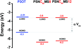 | ||
| Fig. 9 Energy diagram of the HOMO–LUMO energy levels of the active polymers: P3OT, non-diluted PSNC60MS12 (corresponding to 8 vol% of fullerene volume content after dilution), and pure PSNC60MS8. | ||
It should be noticed that, in order to ensure a successful approach and to validate the extrusion concept for the production of solar cells, it was wise to add about 80 vol% of additional PP and PS (which is a high percentage of insulating materials) which decrease the amount of active interface P3OT/PSNC60MS. This explains the high series resistance (3.6 MΩ) and the low current density of cells. The decrease of the current for diluted semiconductor polymers in the presence of an insulating polymer was evidenced in the literature.74,86 In other cases the addition of insulating polymers to the conjugated polymer may lead to improvement of the performances of the optoelectronic device while significantly lowering their cost.74 In contrast, the high shunt resistance (250 MΩ) indicates a good solar cell design (no or very low leakage current) and a performance assembly by lamination.88 Anyway, the detection of a photovoltaic effect for such a system is an extremely promising result that validates the extrusion concept for OPV, and allows considering the extrapolation of this approach to future purely (without insulating phases) active systems with required viscosities.
3. Conclusions and perspectives
This paper demonstrates the successful use of extrusion as a technique for the fabrication of lamellar nanostructured photo-active polymeric films, and suggests a potential application for large scale fabrication of organic photovoltaic solar cells. The originality and novelty of this work first consist in using a one-step continuous extrusion process in order to produce a photo-active nano-multilayer film based on 1024 D (24 nm)/A (24 nm) alternating layers. After this, the total number of D and A nano-layers was increased to 38![[thin space (1/6-em)]](https://www.rsc.org/images/entities/char_2009.gif) 000 (19
000 (19![[thin space (1/6-em)]](https://www.rsc.org/images/entities/char_2009.gif) 000 D/A interfaces) by consolidation of 37 extruded nano-multilayered films. A photovoltaic response was evidenced under light, which confirms the achievement of this functional perfect nano-architectured structure by the extrusion process. The next step, consisting in the use of pure D and A extrudable polymers, should thus lead to high and durable photovoltaic performances and make the extrusion method even competitive.
000 D/A interfaces) by consolidation of 37 extruded nano-multilayered films. A photovoltaic response was evidenced under light, which confirms the achievement of this functional perfect nano-architectured structure by the extrusion process. The next step, consisting in the use of pure D and A extrudable polymers, should thus lead to high and durable photovoltaic performances and make the extrusion method even competitive.
4. Methods and materials
4.1. Materials
The structures of all constituents of the extruded film are presented in Scheme 1. A P3OT/PP blend and a PSNC60MS12/PS blend were used for the elaboration of, respectively, the donor and acceptor extrudable materials. LDPE was used for encapsulation and for stacking of the extruded films by the consolidation method.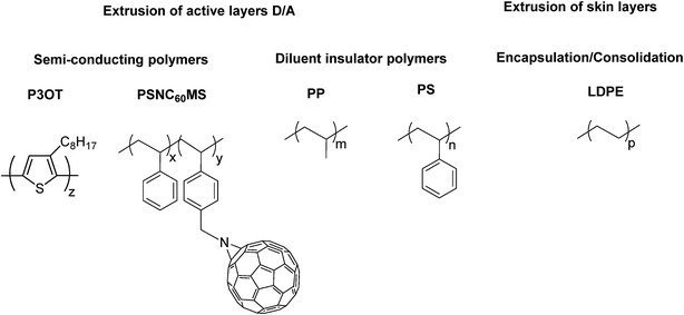 | ||
| Scheme 1 Chemical structures of all used polymeric materials: poly(3-octylthiophene) P3OT, poly(styrene-co-NC60methylstyrene) PSNC60MS12, polypropylene PP, polystyrene PS and polyethylene LDPE. | ||
The poly(3-octylthiophene) polymer (P3OT) with mass-average molecular weight (![[M with combining macron]](https://www.rsc.org/images/entities/i_char_004d_0304.gif) w eq.PS) close to 92 kg mol−1, dispersity (Đ =
w eq.PS) close to 92 kg mol−1, dispersity (Đ = ![[M with combining macron]](https://www.rsc.org/images/entities/i_char_004d_0304.gif) w/
w/![[M with combining macron]](https://www.rsc.org/images/entities/i_char_004d_0304.gif) n) of 1.9 and regioregularity RR ≥ 98.5% was purchased from Rieke Metal. The poly(styrene-co-NC60methylstyrene12) (PSNC60MS12) polymer was laboratory synthesized (
n) of 1.9 and regioregularity RR ≥ 98.5% was purchased from Rieke Metal. The poly(styrene-co-NC60methylstyrene12) (PSNC60MS12) polymer was laboratory synthesized (![[M with combining macron]](https://www.rsc.org/images/entities/i_char_004d_0304.gif) w true = 36 kg mol−1, Đ = 1.7). The synthesis was optimized in our laboratory in small quantities (≈1–2 g) as described in previous reports,70,71 and the large scale production (≈100 g) was subcontracted to Specific Polymers Company. A polypropylene polymer (PP) (MFI at 230 °C-2.16 kg of 12 g/10 min-ASTM D 1238) and a polystyrene polymer (PS) (MFI at 200 °C-5 kg of 30 g/10 min-ISO 1133H) were used as both the diluent (Table 4) and carrier polymers in the coextrusion process. The origin of all constitutive materials for the “D/A nanolayer solar cell” design is summarized in Table 3.
w true = 36 kg mol−1, Đ = 1.7). The synthesis was optimized in our laboratory in small quantities (≈1–2 g) as described in previous reports,70,71 and the large scale production (≈100 g) was subcontracted to Specific Polymers Company. A polypropylene polymer (PP) (MFI at 230 °C-2.16 kg of 12 g/10 min-ASTM D 1238) and a polystyrene polymer (PS) (MFI at 200 °C-5 kg of 30 g/10 min-ISO 1133H) were used as both the diluent (Table 4) and carrier polymers in the coextrusion process. The origin of all constitutive materials for the “D/A nanolayer solar cell” design is summarized in Table 3.
| Elements | Material function | Constituent | Origin |
|---|---|---|---|
| a The nomenclature adopted is P3OT/PP X/Y or PSNC60MS12/PS X/Y, where X and Y are the weight fractions of each constituent. b Synthesized poly(styrene-co-NC60methylstyrene) with 12 vol% of fullerene C60. | |||
| D/A photoactive nano-multilayers | Diluent/carrier | PP | Commercial (Dow Chemical Company PP H700-12) |
| Donor material | P3OT | Commercial (Rieke 4003 E) | |
| Final donor blend | P3OT/PP 65/35a | Blended in an extruder | |
| Diluent/carrier | PS | Commercial (Total Crystal 1960N) | |
| Acceptor material | PSNC60MS12b | Lab synthesis (LEPMI laboratory/specific polymers) | |
| Final acceptor blend | PSNC60MS12/PS 70/30a | Blended in an extruder | |
| Skin layers | Encapsulation & consolidation | LDPE | Commercial (Dow LDPE751A) |
| Anode | Electrode | ITO | Commercial (Ossila S 101) |
| Intermediate layer | Hole transport & adhesive conductive layer | PEDOT–PSS, D-sorbitol, P3HT | Commercial (Ossila P Al4083), commercial (Aldrich, purity 99.9%), commercial (Rieke RMI-001 EE) |
| Cathode | Electrode | InGa eutectic | Commercial (Alfa Aesar, purity 99.9%) |
| Material | Density |
|---|---|
| PP | 0.90 ± 0.01 |
| P3OT | 1.05 ± 0.02 |
| P3OT/PP 65/35 | 0.98 ± 0.01 |
| PS | 1.063 ± 0.005 |
| PSNC60MS12 | 1.08 ± 0.02 |
| PSNC60MS12/PS 70/30 | 1.08 ± 0.03 |
4.2. Methods
Conflicts of interest
There are no conflicts to declare.Acknowledgements
This work was performed within the framework of the Centre of Excellence of Multifunctional Architectured Materials “CEMAM” no. ANR-10-LABX-44-01. The Institut National de l'Energie Solaire (INES) and the financial supports from Assemblée des Pays de Savoie, Université de Savoie are gratefully acknowledged. The authors also thank J. CARR and S. ARMSTRONG for their fruitful help and valuable scientific exchange.References
- W. D. Oosterbaan, V. Vrindts, S. Berson, S. Guillerez, O. Douheret, B. Ruttens, J. D'Haen, P. Adriaensens, J. Manca, L. Lutsen and D. Vanderzande, J. Mater. Chem., 2009, 19, 5424–5435 RSC.
- J. A. Merlo and C. D. Frisbie, J. Phys. Chem. B, 2004, 108, 19169–19179 CrossRef CAS.
- X. Yang and J. Loos, Macromolecules, 2007, 40, 1353–1362 CrossRef CAS.
- J. E. Slota, X. He and W. T. S. Huck, Nano Today, 2010, 5, 231–242 CrossRef CAS.
- D. J. Lipomi, R. C. Chiechi, W. F. Reus and G. M. Whitesides, Adv. Funct. Mater., 2008, 18, 3469–3477 CrossRef CAS.
- F. C. Krebs, Sol. Energy Mater. Sol. Cells, 2009, 93, 394–412 CrossRef CAS.
- G. Ding, Q. Jin, Q. Chen, Z. Hu and J. Liu, Nanoscale Res. Lett., 2015, 10, 1–10 CrossRef CAS PubMed.
- K. Nakano, K. Suzuki, Y. Chen and K. Tajima, Sci. Rep., 2016, 6, 29529 CrossRef CAS PubMed.
- A. Tada, Y. Geng, Q. Wei, K. Hashimoto and K. Tajima, Nat. Mater., 2011, 10, 450–455 CrossRef CAS PubMed.
- C. Poelking, M. Tietze, C. Elschner, S. Olthof, D. Hertel, B. Baumeier, F. Würthner, K. Meerholz, K. Leo and D. Andrienko, Nat. Mater., 2015, 14, 434–439 CrossRef CAS PubMed.
- C. Müller, T. A. M. Ferenczi, M. Campoy-Quiles, J. M. Frost, D. D. C. Bradley, P. Smith, N. Stingelin-Stutzmann and J. Nelson, Adv. Mater., 2008, 20, 3510–3515 CrossRef.
- M. Abbas and N. Tekin, Appl. Phys. Lett., 2012, 101, 073302–073304 CrossRef.
- G. Janssen, A. Aguirre, E. Goovaerts, P. Vanlaeke, J. Poortmans and J. Manca, Eur. Phys. J. Appl. Phys., 2007, 37, 287–290 CrossRef CAS.
- J. Song, C. Du, C. Li and Z. Bo, J. Polym. Sci. Polym. Chem., 2011, 49, 4267–4274 CAS.
- C. V. Hoven, X.-D. Dang, R. C. Coffin, J. Peet, T.-Q. Nguyen and G. C. Bazan, Adv. Mater., 2010, 22, E63–E66 CrossRef CAS PubMed.
- J. K. Lee, W. L. Ma, C. J. Brabec, J. Yuen, J. S. Moon, J. Y. Kim, K. Lee, G. C. Bazan and A. J. Heeger, J. Am. Chem. Soc., 2008, 130, 3619–3623 CrossRef CAS PubMed.
- S. Miller, G. Fanchini, Y.-Y. Lin, C. Li, C.-W. Chen, W.-F. Su and M. Chhowalla, J. Mater. Chem., 2008, 18, 306–312 RSC.
- E. Verploegen, C. E. Miller, K. Schmidt, Z. Bao and M. F. Toney, Chem. Mater., 2012, 24, 3923–3931 CrossRef CAS.
- W. Ma, C. Yang, X. Gong, K. Lee and A. J. Heeger, Adv. Funct. Mater., 2005, 15, 1617–1622 CrossRef CAS.
- M. Campoy-Quiles, T. Ferenczi, T. Agostinelli, P. G. Etchegoin, Y. Kim, T. D. Anthopoulos, P. N. Stavrinou, D. D. C. Bradley and J. Nelson, Nat. Mater., 2008, 7, 158–164 CrossRef CAS PubMed.
- I. Botiz and S. B. Darling, Macromolecules, 2009, 42, 8211–8217 CrossRef CAS.
- U. Stalmach, B. de Boer, C. Videlot, P. F. van Hutten and G. Hadziioannou, J. Am. Chem. Soc., 2000, 122, 5464–5472 CrossRef CAS.
- Y. Kim, S. Cook, S. M. Tuladhar, S. A. Choulis, J. Nelson, J. R. Durrant, D. D. C. Bradley, M. Giles, I. McCulloch, C.-S. Ha and M. Ree, Nat. Mater., 2006, 5, 197–203 CrossRef CAS.
- M. He, F. Qiu and Z. Lin, J. Mater. Chem., 2011, 21, 17039–17048 RSC.
- G. Li, V. Shrotriya, J. Huang, Y. Yao, T. Moriarty, K. Emery and Y. Yang, Nat. Mater., 2005, 4, 864–868 CrossRef CAS.
- F. A. Castro, H. Benmansour, C. F. O. Graeff, F. Nüesch, E. Tutis and R. Hany, Chem. Mater., 2006, 18, 5504–5509 CrossRef CAS.
- D. M. N. M. Dissanayake, A. A. D. T. Adikaari, R. J. Curry, R. A. Hatton and S. R. P. Silva, Appl. Phys. Lett., 2007, 90, 253502 CrossRef.
- J. Y. Park, N. R. Hendricks and K. R. Carter, Langmuir, 2011, 27, 11251–11258 CrossRef CAS PubMed.
- T. Pfadler, M. Coric, C. M. Palumbiny, A. C. Jakowetz, K.-P. Strunk, J. A. Dorman, P. Ehrenreich, C. Wang, A. Hexemer, R.-Q. Png, P. K. H. Ho, P. Müller-Buschbaum, J. Weickert and L. Schmidt-Mende, ACS Nano, 2014, 8, 12397–12409 CrossRef CAS PubMed.
- W. Wiedemann, L. Sims, A. Abdellah, A. Exner, R. Meier, K. P. Musselman, J. L. MacManus-Driscoll, P. Müller-Buschbaum, G. Scarpa, P. Lugli and L. Schmidt-Mende, Appl. Phys. Lett., 2010, 96, 263109 CrossRef.
- F. Yang, M. Shtein and S. R. Forrest, Nat. Mater., 2005, 4, 37–41 CrossRef CAS.
- C. Cocoyer, L. Rocha, L. Sicot, B. Geffroy, R. de Bettignies, C. Sentein, C. Fiorini-Debuisschert and P. Raimond, Appl. Phys. Lett., 2006, 88, 133108 CrossRef.
- S. Zhang, L. Ye, H. Zhang and J. Hou, Mater. Today, 2016, 19, 533–543 CrossRef CAS.
- C. Duan, W. Cai, B. B. Y. Hsu, C. Zhong, K. Zhang, C. Liu, Z. Hu, F. Huang, G. C. Bazan, A. J. Heeger and Y. Cao, Energy Environ. Sci., 2013, 6, 3022–3034 CAS.
- D. J. Burke and D. J. Lipomi, Energy Environ. Sci., 2013, 6, 2053–2066 CAS.
- C. N. Hoth, P. Schilinsky, S. A. Choulis and C. J. Brabec, Nano Lett., 2008, 8, 2806–2813 CrossRef CAS PubMed.
- A. Lange, M. Wegener, C. Boeffel, B. Fischer, A. Wedel and D. Neher, Sol. Energy Mater. Sol. Cells, 2010, 94, 1816–1821 CrossRef CAS.
- J. Yang, D. Vak, N. Clark, J. Subbiah, W. W. H. Wong, D. J. Jones, S. E. Watkins and G. Wilson, Sol. Energy Mater. Sol. Cells, 2013, 109, 47–55 CrossRef CAS.
- R. Søndergaard, M. Hösel, D. Angmo, T. T. Larsen-Olsen and F. C. Krebs, Mater. Today, 2012, 15, 36–49 CrossRef.
- C. Koidis, S. Logothetidis, A. Ioakeimidis, A. Laskarakis and C. Kapnopoulos, Org. Electron., 2013, 14, 1744–1748 CrossRef CAS.
- Y. Liu, T. T. Larsen-Olsen, X. Zhao, B. Andreasen, R. R. Søndergaard, M. Helgesen, K. Norrman, M. Jørgensen, F. C. Krebs and X. Zhan, Sol. Energy Mater. Sol. Cells, 2013, 112, 157–162 CrossRef CAS.
- R. Y. F. Liu, T. E. Bernal-Lara, A. Hiltner and E. Baer, Macromolecules, 2004, 37, 6972–6979 CrossRef CAS.
- T. E. Bernal-Lara, R. Y. F. Liu, A. Hiltner and E. Baer, Polymer, 2005, 46, 3043–3055 CrossRef CAS.
- R. Y. F. Liu, T. E. Bernal-Lara, A. Hiltner and E. Baer, Macromolecules, 2005, 38, 4819–4827 CrossRef CAS.
- F. Ania, F. J. Baltá-Calleja, S. Henning, D. Khariwala, A. Hiltner and E. Baer, Polymer, 2010, 51, 1805–1811 CrossRef CAS.
- Y. Jin, A. Hiltner and E. Baer, J. Polym. Sci. B Polym. Phys., 2007, 45, 1138–1151 CrossRef CAS.
- Y. Jin, A. Hiltner, E. Baer, R. Masirek, E. Piorkowska and A. Galeski, J. Polym. Sci. B Polym. Phys., 2006, 44, 1795–1803 CrossRef CAS.
- R. Y. F. Liu, A. P. Ranade, H. P. Wang, T. E. Bernal-Lara, A. Hiltner and E. Baer, Macromolecules, 2005, 38, 10721–10727 CrossRef CAS.
- R. Y. F. Liu, Y. Jin, A. Hiltner and E. Baer, Macromol. Rapid Commun., 2003, 24, 943–948 CrossRef CAS.
- M. Ponting, A. Hiltner and E. Baer, Macromol. Symp., 2010, 294, 19–32 CrossRef CAS.
- D. R. Paul, Polymer Blends, Elsevier Science, 1978 Search PubMed.
- J. Dooley, Viscoelastic Flow Effects in Multilayer Polymer Coextrusion, Technische Universiteit Eindhoven, 2002 Search PubMed.
- C. D. Han, J. Appl. Polym. Sci., 1973, 17, 1289–1303 CrossRef CAS.
- B. L. Lee and J. L. White, Trans. Soc. Rheol., 1974, 18, 467–492 CAS.
- N. El Kissi, J. M. Piau and R. G. Chaigneau, Rhéologie, 2003, 4, 17 Search PubMed.
- C. D. Han and R. Shetty, Polym. Eng. Sci., 1978, 18, 180–186 CAS.
- H. Mavridis and R. N. Shroff, Polym. Eng. Sci., 1994, 34, 559–569 CAS.
- K. Yoshino, S. Nakajima and R.-I. Sugimoto, Jpn. J. Appl. Phys., 1987, 26, L1038–L1039 CrossRef CAS.
- J. Fanous, M. Schweizer, D. Schawaller and M. R. Buchmeiser, Macromol. Mater. Eng., 2012, 297, 123–127 CrossRef CAS.
- K. Yoshino, S. Nakajima, M. Fujii and R.-I. Sugimoto, Polym. Commun., 1987, 28, 309–310 CAS.
- K. Yoshino, IEEE Trans. Dielectr. Electr. Insul., 1994, 1, 353–364 CrossRef CAS.
- S. Malik and A. K. Nandi, J. Polym. Sci., Part B: Polym. Phys., 2002, 40, 2073–2085 CrossRef CAS.
- G. W. Heffner, W. E. Rochefort and D. S. Pearson, Polym. Eng. Sci., 1995, 35, 868–875 CAS.
- G. W. Heffner, D. S. Pearson and C. L. Gettinger, Polym. Eng. Sci., 1995, 35, 860–867 CAS.
- V. Causin, C. Marega, A. Marigo, L. Valentini and J. M. Kenny, Macromolecules, 2005, 38, 409–415 CrossRef CAS.
- M. Al-Ibrahim, H. K. Roth, M. Schroedner, A. Konkin, U. Zhokhavets, G. Gobsch, P. Scharff and S. Sensfuss, Org. Electron., 2005, 6, 65–77 CrossRef CAS.
- P. Karastatiris, J. A. Mikroyannidis, I. K. Spiliopoulos, A. P. Kulkarni and S. A. Jenekhe, Macromolecules, 2004, 37, 7867–7878 CrossRef.
- C. M. Zimmerman and W. J. Koros, Polymer, 1999, 40, 5655–5664 CrossRef CAS.
- H. Hoppe and N. S. Sariciftci, J. Mater. Res., 2004, 19, 1924–1945 CrossRef CAS.
- A. Nourdine, L. Perrin, R. m. d. Bettignies, S. p. Guillerez, L. Flandin and N. Alberola, Polymer, 2011, 52, 6066–6073 CrossRef CAS.
- L. Perrin, A. Nourdine, E. Planes, C. Carrot, N. Alberola and L. Flandin, J. Polym. Sci., Part B: Polym. Phys., 2013, 51, 291–302 CrossRef CAS.
- H. W. Lee and D. Y. Park, Polymers, 2014, 6, 1057–1073 CrossRef.
- M. E. Nicho, D. Peña-Salgado and P. Altuzar-Coello, Thin Solid Films, 2010, 518, 1799–1803 CrossRef CAS.
- D. Abbaszadeh, A. Kunz, G. A. H. Wetzelaer, J. J. Michels, N. I. Crăciun, K. Koynov, I. Lieberwirth and P. W. M. Blom, Nat. Mater., 2016, 15, 628–633 CrossRef CAS PubMed.
- G. Kaur, R. Adhikari, P. Cass, M. Bown and P. Gunatillake, RSC Adv., 2015, 5, 37553–37567 RSC.
- A. van der Wal, J. J. Mulder and R. J. Gaymans, Polymer, 1998, 39, 5477–5481 CrossRef CAS.
- M. Granstrom, K. Petritsch, A. C. Arias, A. Lux, M. R. Andersson and R. H. Friend, Nature, 1998, 395, 257–260 CrossRef CAS.
- B. Yang, Z. Xiao and J. Huang, Appl. Phys. Lett., 2014, 104, 143304 CrossRef.
- A. Yakimov and S. R. Forrest, Appl. Phys. Lett., 2002, 80, 1667–1669 CrossRef CAS.
- E. Bundgaard and F. C. Krebs, Sol. Energy Mater. Sol. Cells, 2007, 91, 954–985 CrossRef CAS.
- S. H. Park, A. Roy, S. Beaupre, S. Cho, N. Coates, J. S. Moon, D. Moses, M. Leclerc, K. Lee and A. J. Heeger, Nat. Photon., 2009, 3, 297–302 CrossRef CAS.
- B. S. Ong, Y. L. Wu, Y. N. Li, P. Liu and H. L. Pan, Chem.–Eur. J., 2008, 14, 4766–4778 CrossRef CAS PubMed.
- M. Al-Ibrahim, A. Konkin, H.-K. Roth, D. A. M. Egbe, E. Klemm, U. Zhokhavets, G. Gobsch and S. Sensfuss, Thin Solid Films, 2005, 474, 201–210 CrossRef CAS.
- G. Dennler, M. C. Scharber and C. J. Brabec, Adv. Mater., 2009, 21, 1323–1338 CrossRef CAS.
- M. C. Scharber, Adv. Mater., 2016, 28, 1994–2001 CrossRef CAS PubMed.
- X. Yu, K. Xiao, J. Chen, N. V. Lavrik, K. Hong, B. G. Sumpter and D. B. Geohegan, ACS Nano, 2011, 5, 3559–3567 CrossRef CAS PubMed.
- A. Nourdine, L. Perrin, R. d. Bettignies, S. Guillerez, L. Flandin and N. Alberola, Polymer, 2011, 52, 6066–6073 CrossRef CAS.
- J. Huang, G. Li and Y. Yang, Adv. Mater., 2008, 20, 415–419 CrossRef CAS.
| This journal is © The Royal Society of Chemistry 2017 |

