 Open Access Article
Impact of synthetic routes on the structural and physical properties of butyl-1,4-diammonium lead iodide semiconductors†
Majid
Safdari
a,
Dibya
Phuyal
b,
Bertrand
Philippe
 b,
Per H.
Svensson
ae,
Sergei M.
Butorin
b,
Kristina O.
Kvashnina
cd,
Håkan
Rensmo
b,
Lars
Kloo
a and
James M.
Gardner
b,
Per H.
Svensson
ae,
Sergei M.
Butorin
b,
Kristina O.
Kvashnina
cd,
Håkan
Rensmo
b,
Lars
Kloo
a and
James M.
Gardner
 *a
*a
aApplied Physical Chemistry, Department of Chemistry, KTH Royal Institute of Technology, SE-10044, Stockholm, Sweden. E-mail: jgardner@kth.se; james.m.gardner@gmail.com
bDept. of Physics and Astronomy, Uppsala Univ., Box 516, SE-75121, Uppsala, Sweden
cESRF-The European Synchrotron, CS40220, 38043 Grenoble Cedex 9, France
dHelmholtz Zentrum Dresden-Rossendorf, Institute of Resource Ecology, 01314 Dresden, Germany
eSP Process Development, Forskargatan, 15121 Södertälje, Sweden
First published on 23rd January 2017
Abstract
We report the significant role of synthetic routes and the importance of solvents in the synthesis of organic–inorganic lead iodide materials. Through one route, the intercalation of dimethylformamide in the crystal structure was observed leading to a one--dimensional (1D) [NH3(CH2)4NH3]Pb2I6 structure of the product. This product was compared with the two-dimensional (2D) [NH3(CH2)4NH3]PbI4 recovered from aqueous solvent based synthesis with the same precursors. UV-visible absorption spectroscopy showed a red-shift of 0.1 eV for the band gap of the 1D network in relation to the 2D system. This shift primarily originates from a shift in the valence band edge as determined from photoelectron- and X-ray spectroscopy results. These findings also suggest the iodide 5p orbital as the principal component in the density of states in the valence band edge. Single crystal data show a change in the local coordination around iodide, while in both materials, lead atoms are surrounded by iodide atoms in octahedral units. The conductivity of the one-dimensional material ([NH3(CH2)4NH3]Pb2I6) was 50% of the two-dimensional material ([NH3(CH2)4NH3]PbI4). The fabricated solar cells reflect these changes in the chemical and electronic structure of both materials, although the total light conversion efficiencies of solar cells based on both products were similar.
Introduction
The growing interest in the application of organic–inorganic metal halides in optical devices has inspired the development of new materials. During recent years, the three-dimensional perovskite material methylammonium lead(II) iodide, (MA)PbI3, has been promoted as a light-absorber in photovoltaics. The perovskite (MA)PbI3 has a Pm3m space group containing a primitive cubic unit cell.1,2 Unlike many semiconductors, films of highly crystalline (MA)PbI3 may be generated through solution-based processes. In addition, (MA)PbI3 has a direct band gap of 1.55 eV and high extinction coefficients, which make this material an interesting candidate for solar cell applications. Although competing with existing solar cell technologies is challenging, researchers have reported exciting efficiencies up to 22.1% efficiency for solid-state solar cells based on methylammonium/formamidinium lead(II) iodide.3–8 The first reported use of (MA)PbI3 in solar cells was as a dye in liquid junction dye-sensitized solar cells;3 however, the solar cells suffered from very low stability due to the high solubility of the methylammonium cation in the liquid electrolyte. Subsequently, the liquid electrolyte has been replaced with solid hole-transport materials (HTM), which have increased solar cell stability.4–8 However, atmospheric moisture causes decomposition of the perovskite on the time scale of hours due, primarily, to the hydrophilicity of the cations.9,10 It is the lack of the long-term stability of these perovskite films that impedes progress in the industrialization of these solar cells.11–13While Pb2+ is known to be toxic and a risk to human health, a life cycle assessment study of (MA)PbI3 perovskite solar cells reported by Espinosa N. et al.14 showed that the contribution of methylammonium iodide to human health risk was surprisingly far higher than the contribution from Pb. Due to health concerns and instability issues, there is a clear need for alternatives to methylammonium lead iodide for use in solar cells. For substitution of the lead, the closest candidate would be tin. Several successful attempts at producing solar cells with Sn instead of Pb have yielded solar cell efficiencies of over 6%.15,16 Tin- and lead-based perovskites have very similar structural properties, which implies the importance of the structure of these materials with respect to their impressive physical properties. In our previous reports, we have reported relations between the structure of organic–inorganic lead halide materials and their physical properties.2,17 By changing organic cations to more stable cations, we correlate the change of dimensionality of these materials with their function as light absorbers in solid-state solar cells.2,17
The effect of synthetic routes on the three-dimensional (3D) methylammonium lead/tin iodide perovskite has been reported by Stoumpos C. C. et al., which shows a high dependency of the chemical and physical properties of the product on the synthetic routes.18 Furthermore, significant improvement in the efficiency has been achieved by the solvent engineering effect on the light absorber layer of the perovskite solar cells.19,20 Our interest arose from these findings and our previous reports for further studies of these materials.
Herein, we report the strong effect of the synthetic route on the structure and properties of butyl-1,4-diammonium lead(II) iodide materials. Through two different synthetic routes, we have utilized butyl-1,4-diammonium iodide [NH3(CH2)4NH3]I2 as a bication and anion source when mixed with lead iodide (PbI2) to produce [NH3(CH2)4NH3]PbI4 and [NH3(CH2)4NH3]Pb2I6. We investigated the structure of the products leading to two completely different structures: two-dimensional (2D) perovskite planes and one-dimensional (1D) non-perovskite chains. The structural differences of the crystals were confirmed by obtaining different X-ray powder diffraction patterns for the bulk material. These structural characterizations were followed by physical characterizations. Absorption spectra of the materials show a shift in the absorption band edge. The electronic structures of [NH3(CH2)4NH3]PbI4 and [NH3(CH2)4NH3]Pb2I6 were studied by synchrotron-based X-ray spectroscopic methods. Solar cells were fabricated based on the two materials and utilized as light absorbers in solar cells; similar power conversion efficiencies of 1.1% were obtained for [NH3(CH2)4NH3]PbI4/(BdA)PbI4 based solid state solar cells and [NH3(CH2)4NH3]Pb2I6/(BdA)Pb2I6 solar cells.
Experimental section
The precursors used in this work were all commercially available products and used without further purification. 1,4-Diaminobutane (99%), lead(II) iodide (99.999%), diethyl ether (≥99.0%), and dimethylformamide (DMF) (purity ≥ 99%) were purchased from Sigma-Aldrich. Spiro-OMeTAD (2,20,7,70-tetrakis[N,N-di(4-methoxyphenyl)amino-9,9′-spirobifluorene], purity ≥ 99.5 HPLC) was purchased from Xi'an Polymer Light Technology Corp. Dyesol (18NRT) TiO2 paste was used and hydriodic acid was purchased from Alfa Aesar, 57% w/w aqueous solution stabilized with 1.5% hypophosphorous acid.Synthesis
For the synthesis of butyl-1,4-diammonium iodide, the previous procedure has been followed.17 Briefly, 1 mole equivalent of 1,4-diaminobutane (BA) (0.003 M, 0.264 g) was mixed with 2 mole equivalents of HI (0.006 M, 1.3703 g) for 2 hours. [NH3(CH2)4NH3]I2/(BdA)I2 was recovered by solvent evaporation and washed with diethyl ether (yield 89%).One-dimensional [NH3(CH2)4NH3]Pb2I6/(BdA)Pb2I6 was synthesized by mixing 1 mole equivalent of (BdA)I2 (0.0015 M, 0.516 g) with 2 mole equivalents of PbI2 (0.003 M, 1.383 g) in DMF (5 mL). Of the resulting solution, 1 mL was used for crystal growth with toluene as the anti-solvent. The remaining part of the solution was used to recover (BdA)Pb2I6 powder by evaporation of the solvent at 50 °C using a rotary evaporator (yield 92%).
The two-dimensional perovskite, [NH3(CH2)4NH3]PbI4/(BdA)PbI4, was synthesized according to the previous report.17 Briefly, 2 mole equivalents of PbI2 (0.003 M, 1.383 g) were dissolved in 4 mL HI solution. 1 mole equivalent of (BdA)I2 (0.0015 M, 0.516 g) was dissolved in 3 mL excess HI. The two solutions were mixed and stirred at 90 °C for 1 hour. In order to grow single crystals of the material, after half of the solvent is evaporated, the magnetic stir bar was taken out from the solution and the temperature was gradually decreased (5 °C h−1) to −10 °C. Single crystals were obtained after keeping the solution at −10 °C for 24 hours. Crystals were recovered from the solution and used for crystallography. After removing the single crystals, the residual precipitate was washed with diethyl ether and used for further characterization (yield 81%).
Characterization
![[thin space (1/6-em)]](https://www.rsc.org/images/entities/char_2009.gif) :
:![[thin space (1/6-em)]](https://www.rsc.org/images/entities/char_2009.gif) 3.5
3.5![[thin space (1/6-em)]](https://www.rsc.org/images/entities/char_2009.gif) :
:![[thin space (1/6-em)]](https://www.rsc.org/images/entities/char_2009.gif) TiO2 Dyesol paste
TiO2 Dyesol paste![[thin space (1/6-em)]](https://www.rsc.org/images/entities/char_2009.gif) :
:![[thin space (1/6-em)]](https://www.rsc.org/images/entities/char_2009.gif) 99.5% ethanol) was spincoated onto a microscope slide followed by sintering at 500 °C. A solution of 0.5 M (BdA)Pb2I6 or (BdA)PbI4 in DMF was spincoated on the substrate followed by heating at 90 °C for 10 min. UV-visible absorption measurements were performed using a UV-Visible Cary 300 spectrophotometer.
99.5% ethanol) was spincoated onto a microscope slide followed by sintering at 500 °C. A solution of 0.5 M (BdA)Pb2I6 or (BdA)PbI4 in DMF was spincoated on the substrate followed by heating at 90 °C for 10 min. UV-visible absorption measurements were performed using a UV-Visible Cary 300 spectrophotometer.
 | (1) |
![[thin space (1/6-em)]](https://www.rsc.org/images/entities/char_2009.gif) :
:![[thin space (1/6-em)]](https://www.rsc.org/images/entities/char_2009.gif) 4.5 wt% ratio of TiO2 Dyesol paste with ethanol was used to spincoat a layer of TiO2 on top of the blocking layer at a rate of 4000 rpm. This was followed by sintering at 500 °C for 30 min. A light absorbing layer was produced by spincoating 0.5 M dimethylformamide (DMF; ≥99%) precursor solutions of the materials on the TiO2 films and then the films were annealed at 90 °C for 10 min.
4.5 wt% ratio of TiO2 Dyesol paste with ethanol was used to spincoat a layer of TiO2 on top of the blocking layer at a rate of 4000 rpm. This was followed by sintering at 500 °C for 30 min. A light absorbing layer was produced by spincoating 0.5 M dimethylformamide (DMF; ≥99%) precursor solutions of the materials on the TiO2 films and then the films were annealed at 90 °C for 10 min.
A solution of 80 mM SpiroOMeTAD, 200 mM 4-tert-butylpyridine (TBP, 99%) and 30 mM bis(trifluoromethane) sulfonimide lithium salt (LiTFSI, 99%, Io-li-tec) was prepared. The solvent for this solution was a mixture of 80 wt% chlorobenzene, 10 wt% acetonitrile (99.8%), and 10 wt% 1,1,2,2-tetrachloroethane (TeCA). The hole transporting (HTM) layer was prepared through the spincoating of this solution at 2000 rpm for 30 seconds. Finally, as the back contact, an 80-nm thick layer of gold was deposited by thermal evaporation.2,4,6,7 All of the fabrication steps (except the gold evaporation) were performed in an ambient environment (at 22 °C with a humidity of 46% as measured by using an AMPROBE TH-3 hygrometer).
Solar cell characterization
Results and discussion
Material characterization and crystal growth
The most popular and convenient route for the synthesis of the organic–inorganic lead(II) halide materials is through the solution methods. Through these methods, usually, lead halide will be mixed with the halide salt of organic cations/bications (see Fig. 1).5,26 A solvent will be added, and the synthesis will be done by heating and stirring this mixture for hours. To obtain the product, the influence of the solvent will be reduced by evaporation of the solvent or gradual cooling. This will generally result in the precipitation of the most thermodynamically stable product. This precipitation is normally governed by several important factors, e.g. (1) the Lewis acid and base activity of the components, (2) the iodide to lead ratio and (3) the tendency of the solvent to incorporate into the structure of the product. Diverse possible structures can be obtained for the products based on the cation/bication size, the ionic radius of the main metal, and the solvent activity. The dimensionality of the product can vary from zero-dimensional isolated units up to three-dimensional networks. This structural complexity provides a considerable opportunity for scientific research on material design and their properties. On the other hand, the reaction may result in an undesirable product, based on the diversity of the possible products. | ||
| Fig. 1 General solution-based synthetic procedure for organic–inorganic lead halide materials, and (b) the synthetic routes for preparation of the (BdA)PbI4 and (BdA)Pb2I6. | ||
The solvent effect is significant in determining the material structure and has been highlighted before.19 The great impact of the solvent on the perovskite deposition and architecture of the perovskite layer has been pointed out as a part of solar cell efficiency improvement.19,20 In the previous reports on the application of (MA)PbI3, the mixture of lead iodide with methyl ammonium iodide was stirred at 60 °C for 12 hours.4,26 These reports have been followed by further developments in solar cell optimization that have lead to the use of mixed solvents, e.g. g-butyrolactone/dimethylsulfoxide (GBL/DMSO) or dimethylformamide/dimethylsulfoxide (DMF/DMSO). These reports have proved that the crystallinity of the perovskite layer would be highly affected by the tendency of the solvent to evaporate versus to incorporate into the structure.15,24
Single crystal data
Through the single crystal characterizations, two different structures were obtained for these materials. For the product of Route 1 (BdA)Pb2I6, a one-dimensional inorganic chain was obtained with a disordered intercalation of organic bications and solvent in between (see Fig. 2A). The inorganic chains in the (BdA)Pb2I6 chemical structure consist of face-sharing lead iodide octahedral units. The space group of P1 was found for the solvate-incorporated structure. The distance between the inorganic structural chains through space (Pb–Pb distance) varies from 10.24 Å to 13.04 Å. The oxygen atoms of the DMF are at a distance of 3.98 Å to 6.2 Å indicating a very weak bonding interaction with the inorganic chains. The intercalation of the solvent in the chemical structure of organic–inorganic metal halide materials is a known phenomenon,27 which has a significant impact on the physical properties of these materials.19,20 For the larger cations/bications, the distance between the inorganic structural units is longer, which accommodates larger vacancies between lead iodide chains that may be occupied by the solvent. The molecular volume of the (BdA) bication is substantially larger than the methylammonium cation and causes the connectivity of the inorganic units to be lost in one or more dimensions for the perovskite network. As well, bulkier cations/bications will increase the through-space distance between inorganic lead iodide units. This finding is consistent with our previous report, wherein the propylammonium lead(II) iodide structure incorporates gamma-butyrolactone due to the empty space between lead iodide chains. For the product of Route 2, a two-dimensional perovskite structure was produced. Details of this structure have been previously reported.17 Briefly, it can be mentioned here that (BdA)PbI4 (001) structural planes were found to consist of octahedral corner sharing lead iodide planes and organic bications (BdA) as separating bridges between them (see Fig. 2B). The intra-chain Pb–Pb distances in (BdA)Pb2I6 vary between 4.00 Å and 4.07 Å. This can be compared with the same distance in the two-dimensional (BdA)PbI4 structure which is 6.08 Å to 6.16 Å. Comparing Pb–I–Pb angles, for (BdA)Pb2I6 the angles varied from 76.6 to 78.2 degrees while for BdAPbI4 they varied from 146.3 to 146.4 degrees. The changing Pb–I–Pb bond angles between (BdA)Pb2I6 and (BdA)PbI4 suggest that the orbitals that contribute to the bonding of these materials may be different.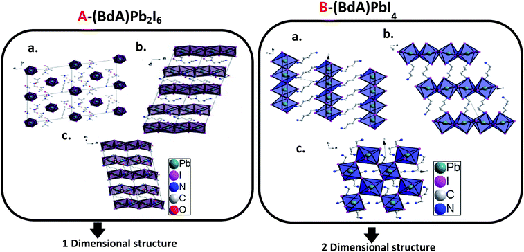 | ||
| Fig. 2 Crystal structure of (A) solvated (BdA)Pb2I6 and (B) (BdA)PbI4 (ref. 17) along three axes. | ||
The structural differences between (BdA)Pb2I6 and (BdA)PbI4 were confirmed by X-ray powder diffraction on the recovered powders (see Fig. 3). Different peaks were obtained for the 1D (BdA)Pb2I6 compared to the 2D (BdA)PbI4, illustrating structural changes in the bonding environment of the lead and iodide in each material. Several peaks were shifted to the lower angles for 1D compared to 2D. We attributed these peaks to the increasing volume of the unit cell for 1D (BdA)Pb2I6 (1968.27 Å3) as compared to 2D (BdA)PbI4 (765.28 Å3). The powder diffraction patterns show the poly-crystallinity of both samples although some broad peaks were recorded. These broad peaks can be due to some structural disorder in the powder samples. Similar phenomena were observed for previous two-dimensional materials.17 Shifts in the powder-XRD relative to the single-crystal data for (BdA)Pb2I6 suggest that the powdered material has a smaller unit volume than a single crystal. We attribute this to solvent loss from the powdered crystals of (BdA)Pb2I6. The solvent is lost during the annealing process and results in a unit cell contraction (Fig. S7†).
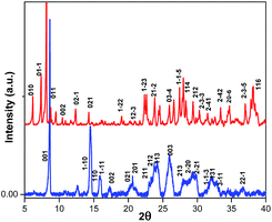 | ||
Fig. 3 Powder diffraction patterns for the  (BdA)PbI4 and (BdA)PbI4 and  (BdA)Pb2I6. Miller indices were obtained from single crystal data. (BdA)Pb2I6. Miller indices were obtained from single crystal data. | ||
UV-vis absorption spectroscopy
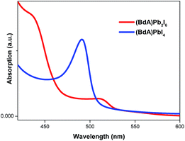
Characterization of absorption properties for the two different samples was performed and the obtained spectra are presented in Fig. 4. The first observed absorption peak was attributed to the band gap absorption between the valence and conduction bands. The direct band gap Tauc formula was used for the estimation of the band gap values of (BdA)Pb2I6 and (BdA)PbI4.28 A red shift of 0.1 eV in the absorption edge position was observed for the one-dimensional non-perovskite (BdA)Pb2I6 when compared to the two-dimensional perovskite (BdA)PbI4. Extrapolation of the absorption edge from the Tauc plot (Fig. S8†) suggests band gap values of 2.28 eV and 2.37 eV for (BdA)Pb2I6 and (BdA)PbI4, respectively. Based on the intensity of the transition, the apparent absorption coefficient decreased for (BdA)Pb2I6 compared to (BdA)PbI4. A lower extinction coefficient for the solvated structure was observed for the methylammonium tin iodide perovskite27 and also for the formamidinium lead iodide perovskite.29 Based on most of the previous studies,2,27,30 the band gap is expected to be higher for one-dimensional materials compared to higher dimensionality systems. But in this particular study, the absorption study showed rather small effects in the opposite direction. These interesting findings motivate us to analyze the electronic structure of these materials.Conductivity
The conductivity of (BdA)Pb2I6 was recorded as 5.3 × 10⁻⁶ S cm−1 compared to 1.3 × 10⁻⁵ S cm−1 for (BdA)PbI4.17 We explain these data based on the chemical structure and dimensionalities of the two materials. In (BdA)PbI4, charge conduction occurs through the lead iodide planes, while for (BdA)Pb2I6 connectivity and charge transport are solely along lead iodide chains. The finding supports previous evidence showing a high dependence of conductivity on the structural dimensionality.2X-ray based spectroscopy
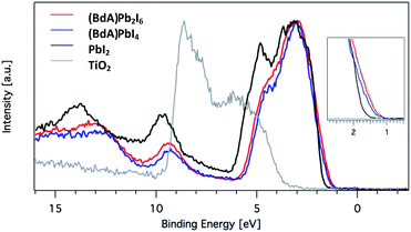
An appropriate estimation of sample stoichiometry can be made by measuring intensities from the core levels of I 4d and Pb 5d (Fig. S2†). This estimation takes into account the differential atomic subshell photoionization cross-sections as well as comparison of similar orbitals. On the basis of these cross-section adjustments, we experimentally obtain appropriate relative intensities that are in accordance with what is expected from the stoichiometry of PbI2, (BdA)Pb2I6 and (BdA)PbI4 (see Table 1). For both (BdA)Pb2I6 and (BdA)PbI4, the magnitude of the Pb 4f core-level shifts is quite small (0.05 eV); however, for I 3d, the core-level shift for (BdA)Pb2I6 and (BdA)PbI4 is 0.12 eV. The experimental data give evidence that the positions of the valence positions shift largely due to the iodine p orbitals. The two butyldiammonium lead(II) iodide materials under study have geometrical configurations that are quite different from each other. The local bonding environment of iodine, which is connected by 1-dimensional face-sharing chains or 2-dimensional corner-sharing planes, indicates a distinct local arrangement that can explain the subtle differences in the electronic structure. This can be experimentally verified by probing iodine states specifically through absorption and emission spectroscopy.
![[S with combining low line]](https://www.rsc.org/images/entities/char_0053_0332.gif) ![[a with combining low line]](https://www.rsc.org/images/entities/char_0061_0332.gif) ![[m with combining low line]](https://www.rsc.org/images/entities/char_006d_0332.gif) ![[p with combining low line]](https://www.rsc.org/images/entities/char_0070_0332.gif) ![[l with combining low line]](https://www.rsc.org/images/entities/char_006c_0332.gif) ![[e with combining low line]](https://www.rsc.org/images/entities/char_0065_0332.gif) |
Chemical formula | I/Pb ratio |
|---|---|---|
| (BdA)Pb2I6 | [NH3(CH2)4NH3]Pb2I6 | 2.65 |
| BdAPbI4 | [NH3(CH2)4NH3]PbI4 | 3.84 |
| Lead iodide | PbI2 | 1.78 |
Here, we explore the ability of high energy resolution fluorescence detection (HERFD) X-ray absorption near edge structure (XANES) and resonant inelastic X-ray scattering (RIXS) spectroscopy to distinguish between our similar but dimensionally varied samples. Fig. 7 shows the experimental HERFD–XANES spectra (left) and RIXS spectra (right) for this set. XANES probes the unoccupied density of states of the studied element. In our case (BdA)Pb2I6 and (BdA)PbI4 clearly have different local geometries in the structure of the unoccupied iodine states. This indicates that there is a modification in the atomic position of neighbors, such as bond lengths and angles. This is entirely expected, since the local geometry of iodine is what sets these two samples apart in contrast to Pb, which lies in a similar octahedral cage.
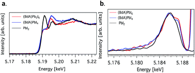 | ||
Fig. 7 (a) Plots of the unoccupied np states of iodine in the conduction band and (b) RIXS spectra for  (BdA)Pb2I6, (BdA)Pb2I6,  (BdA)PbI4, and (BdA)PbI4, and  PbI2. PbI2. | ||
The iodide atoms have distinct bonding environments; therefore, one can expect to observe a different spectral character in the high energy XANES region. RIXS spectra are dominated by dipole-allowed transitions originating from occupied iodine 5p orbitals, probing only occupied states, thus giving us a partial density of states near the VB edge. We see spectral features that are unique to our samples in contrast to PbI2, in particular a shoulder feature on the higher energy side. This is a consequence of structural changes due to iodine orbitals, which are involved in a different degree of hybridization with Pb 6s orbitals. The observed subtle shift to higher energies for (BdA)Pb2I6 in both HAXPES VB and iodine RIXS indicates that the observed change in the electronic structure of the valence band is primarily due to the iodine orbitals.
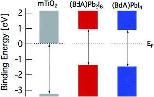
The band diagram of the materials obtained from spectroscopic data is presented in Fig. 8. The valence band edge is obtained from PES data with the Fermi level set to 0 eV in accordance with the Au Fermi level. The position of the conduction band minimum (CBM) relative to EF is estimated by subtracting the optical band gap from the valence band maximum (VBM). From this picture, a suitable combination of our materials can be utilized in many different device architectures for efficient charge extraction.
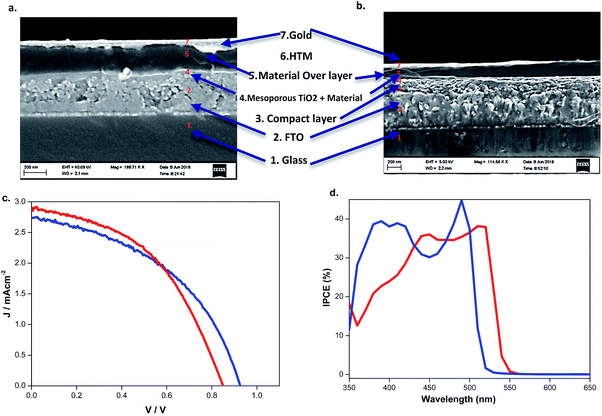
| Eff. (%) | V oc (mV) | J sc (mA cm−2) | FF | APCE (%) | Band gap (eV) | Conductivity (S cm−1) | |
|---|---|---|---|---|---|---|---|
| BdAPbI4 | 1.1 | 925 | 2.73 | 0.45 | 36 | 2.37 | 1.3 × 10⁻⁵ |
| BdAPb2I6 | 1.1 | 845 | 2.98 | 0.45 | 35 | 2.28 | 5.3 × 10⁻⁶ |
Conclusion
The effects of solvents and synthetic routes of butyldiammonium lead iodide were investigated through the characterization of the two products. Chemical and electronic structures were studied in detail. Dimethylformamide showed a tendency to intercalate into the crystal structure and change the chemical structure of the final product to a one-dimensional structure. The impacts of the structural changes on the physical properties were deeply studied. A small red shift for the band edge was observed for one-dimensional (BdA)Pb2I6 compared to two-dimensional (BdA)PbI4. This shift in the band edge was confirmed by IPCE measurements on the solar cells using the two materials as light absorbing layers. Through X-ray based spectroscopies, it was determined that the shift in the band gap mostly originates from changes in the valence band. HERFD–XANES and XPS studies suggest that for both materials the dominant contribution to the valence band comes from the iodine 5p orbital while the lead 6s orbital is the primary contribution to the conduction band. Through the transmission of the chemical structure from two-dimensional to one-dimensional, the chemical environment and bonding of iodide atoms will be mostly altered while lead atoms remain in the center of octahedral units with minor changes in the distance to the iodide corners. The HERFD–XANES and XPS findings confirm these structural changes by showing a large change in the valence band edge position compared to small changes in conduction band edges. The conductivity of the one-dimensional material, (BdA)Pb2I6, was half that of the two-dimensional material, (BdA)PbI4. The decrease in conductivity indicates the importance of connectivity for maintaining electron conductivity throughout the material. Coincidentally, the fabricated solar cells based on the two materials showed similar efficiencies, despite the substantial differences in the chemical structure and absorption properties that affect the recorded voltages and current densities.Acknowledgements
This work was supported by the Swedish Government through “STandUP for ENERGY”, the Swedish Energy Agency, the Swedish Research Council, Knut & Alice Wallenberg Foundation, and the National Research Foundation of Korea (NRF-2014K1A3A1A47067328).References
- T. Baikie, Y. Fang, J. M. Kadro, M. Schreyer, F. Wei, S. G. Mhaisalkar, M. Graetzel and T. J. White, J. Mater. Chem. A, 2013, 1, 5628–5641 CAS.
- M. Safdari, A. Fischer, B. Xu, L. Kloo and J. M. Gardner, J. Mater. Chem. A, 2015, 3, 9201–9207 CAS.
- A. Kojima, K. Teshima, Y. Shirai and T. Miyasaka, J. Am. Chem. Soc., 2009, 131, 6050–6051 CrossRef CAS PubMed.
- H.-S. Kim, C.-R. Lee, J.-H. Im, K.-B. Lee, T. Moehl, A. Marchioro, S.-J. Moon, R. Humphry-Baker, J.-H. Yum, J. E. Moser, M. Gratzel and N.-G. Park, Sci. Rep., 2012, 2, 591 Search PubMed.
- M. M. Lee, J. Teuscher, T. Miyasaka, T. N. Murakami and H. J. Snaith, Science, 2012, 338, 643–647 CrossRef CAS PubMed.
- J. Burschka, N. Pellet, S.-J. Moon, R. Humphry-Baker, P. Gao, M. K. Nazeeruddin and M. Gratzel, Nature, 2013, 499, 316–319 CrossRef CAS PubMed.
- W. S. Yang, J. H. Noh, N. J. Jeon, Y. C. Kim, S. Ryu, J. Seo and S. I. Seok, Science, 2015, 348, 1234–1237 CrossRef CAS PubMed.
- http://www.nrel.gov/ncpv/images/efficiency_chart.jpg .
- J. Yang, B. D. Siempelkamp, D. Liu and T. L. Kelly, ACS Nano, 2015, 9, 1955–1963 CrossRef CAS PubMed.
- S. Pathak, A. Sepe, A. Sadhanala, F. Deschler, A. Haghighirad, N. Sakai, K. C. Goedel, S. D. Stranks, N. Noel, M. Price, S. Hüttner, N. A. Hawkins, R. H. Friend, U. Steiner and H. J. Snaith, ACS Nano, 2015, 9, 2311–2320 CrossRef CAS PubMed.
- T. A. Berhe, W.-N. Su, C.-H. Chen, C.-J. Pan, J.-H. Cheng, H.-M. Chen, M.-C. Tsai, L.-Y. Chen, A. A. Dubale and B.-J. Hwang, Energy Environ. Sci., 2016, 9, 323–356 CAS.
- X. Li, M. Ibrahim Dar, C. Yi, J. Luo, M. Tschumi, S. M. Zakeeruddin, M. K. Nazeeruddin, H. Han and M. Grätzel, Nat. Chem., 2015, 7, 703–711 CrossRef CAS PubMed.
- D. Wang, M. Wright, N. K. Elumalai and A. Uddin, Sol. Energy Mater. Sol. Cells, 2016, 147, 255–275 CrossRef CAS.
- N. Espinosa, L. Serrano-Luján, A. Urbina and F. C. Krebs, Sol. Energy Mater. Sol. Cells, 2015, 137, 303–310 CrossRef CAS.
- N. K. Noel, S. D. Stranks, A. Abate, C. Wehrenfennig, S. Guarnera, A.-A. Haghighirad, A. Sadhanala, G. E. Eperon, S. K. Pathak, M. B. Johnston, A. Petrozza, L. M. Herz and H. J. Snaith, Energy Environ. Sci., 2014, 7, 3061–3068 CAS.
- F. Hao, C. C. Stoumpos, D. H. Cao, R. P. H. Chang and M. G. Kanatzidis, Nat. Photonics, 2014, 8, 489–494 CrossRef CAS.
- M. Safdari, P. H. Svensson, M. T. Hoang, I. Oh, L. Kloo and J. M. Gardner, J. Mater. Chem. A, 2016, 4(40), 15638–15646 CAS.
- C. C. Stoumpos, C. D. Malliakas and M. G. Kanatzidis, Inorg. Chem., 2013, 52, 9019–9038 CrossRef CAS PubMed.
- N. J. Jeon, J. H. Noh, Y. C. Kim, W. S. Yang, S. Ryu and S. I. Seok, Nat. Mater., 2014, 13, 897–903 CrossRef CAS PubMed.
- Y. Rong, Z. Tang, Y. Zhao, X. Zhong, S. Venkatesan, H. Graham, M. Patton, Y. Jing, A. M. Guloy and Y. Yao, Nanoscale, 2015, 7, 10595–10599 RSC.
- B. A. B. S. Apex II, Bruker AXS Inc., Madison, WI, USA, 2013 Search PubMed.
- M. Gorgoi, S. Svensson, F. Schäfers, G. Öhrwall, M. Mertin, P. Bressler, O. Karis, H. Siegbahn, A. Sandell, H. Rensmo, W. Doherty, C. Jung, W. Braun and W. Eberhardt, Nuclear Instruments and Methods in Physics Research Section A: Accelerators, Spectrometers, Detectors and Associated Equipment, 2009, 601, 48–53 CrossRef CAS.
- J. Scofield, J. Electron Spectrosc. Relat. Phenom., 1976, 8, 129–137 CrossRef CAS.
- C. Gauthier, V. A. Sole, R. Signorato, J. Goulon and E. Moguiline, J. Synchrotron Radiat., 1999, 6, 164–166 CrossRef CAS PubMed.
- A. J. Atkins, C. R. Jacob and M. Bauer, Chem.–Eur. J., 2012, 18, 7021–7025 CrossRef CAS PubMed.
- J.-H. Im, C.-R. Lee, J.-W. Lee, S.-W. Park and N.-G. Park, Nanoscale, 2011, 3, 4088–4093 RSC.
- F. Hao, C. C. Stoumpos, P. Guo, N. Zhou, T. J. Marks, R. P. H. Chang and M. G. Kanatzidis, J. Am. Chem. Soc., 2015, 137, 11445–11452 CrossRef CAS PubMed.
- J. Tauc, R. Grigorovici and A. Vancu, Phys. Status Solidi B, 1996, 15, 10 Search PubMed.
- T. M. Koh, K. Fu, Y. Fang, S. Chen, T. C. Sum, N. Mathews, S. G. Mhaisalkar, P. P. Boix and T. Baikie, J. Phys. Chem. C, 2014, 118, 16458–16462 CAS.
- D. B. Mitzi, in Progress in Inorganic Chemistry, John Wiley & Sons, Inc., 2007, pp. 1–121 Search PubMed.
- J. Endres, D. A. Egger, M. Kulbak, R. A. Kerner, L. Zhao, S. H. Silver, G. Hodes, B. P. Rand, D. Cahen, L. Kronik and A. Kahn, J. Phys. Chem. Lett., 2016, 7, 2722–2729 CrossRef CAS PubMed.
- E. L. Unger, E. T. Hoke, C. D. Bailie, W. H. Nguyen, A. R. Bowring, T. Heumuller, M. G. Christoforo and M. D. McGehee, Energy Environ. Sci., 2014, 7, 3690–3698 CAS.
Footnote |
| † Electronic supplementary information (ESI) available: Fig. S1–S9, Tables S1 and S2 including more detailed structural information, Tauc plot, detailed IV data, IV hysteresis, histogram of solar cell data. See DOI: 10.1039/c6ta10123b |
| This journal is © The Royal Society of Chemistry 2017 |

