A novel liquid metal patterning technique: voltage induced non-contact electrochemical lithography at room temperature†
Zhenwei
Yu
 ,
Frank F.
Yun
 and
Xiaolin
Wang
*
Institute for Superconducting and Electronic Materials, Australian Institute for Innovative Materials, University of Wollongong, Wollongong, NSW 2500, Australia. E-mail: xiaolin@uow.edu.au
First published on 17th November 2017
Abstract
Non-contact, maskless, voltage induced electrochemical lithography for liquid metals was demonstrated at room temperature. Various patterns in liquid metal can be simply and rapidly fabricated using electrochemical hole/dot matrix printing, continuous “writing” and a movable type printing method.
Conceptual insightsIn this communication, we report for the first time a new patterning method, voltage induced electrochemical lithography for liquid metals at room temperature, which is non-contact, maskless, and material-reusable. Various patterns in liquid metal can be simply fabricated using electrochemical hole/dot matrix printing, and continuous “writing”. The voltage induced electrochemical lithography for liquid metal mimics existing patterning techniques such as conventional lithography, laser engraving, and inkjet printing techniques. Remarkably, it is possible to pattern a liquid metal using the movable type printing method, which is a unique advantage over existing liquid metal patterning methods. Our findings offer novel liquid metal patterning techniques for further development of liquid metal applications in electronics, optics, and microfluidics. |
Room temperature gallium based liquid metals are set to play a significant role in various applications due to their high electrical and thermal conductivity, negligible vapor pressure, and low viscosity.1–9 Most importantly, they are less toxic as compared to mercury. Novel phenomena characteristic of gallium and gallium based alloys include giant deformation and transformation caused by significant changes in the surface tension of liquid metals due to the formation or removal of oxide on the liquid metal surface under the application of a voltage.10–13 Recently intensive research efforts on these new phenomena have led to the development of emerging applications, including liquid metal enabled pumps,12,14 tunable antennas,15–18 microelectromechanical system (MEMS) devices,19–23 and liquid metal robots.24–27 We have recently demonstrated spontaneous fast deformation and solidification in supercooled liquid gallium induced by both voltage and nucleation on the electrode.13
Patterning of liquid metals has attracted intense interest for applications such as microfluidic electrodes,28–30 sensors,24,31,32 stretchable electronics,33–37 and reconfigurable circuits.19,38 Two-dimensional (2D) patterning of liquid metals can be enabled through methods such as masked deposition,39 direct laser patterning,40 inkjet printing,41 and conventional lithography.42 The three-dimensional (3D) shaping of liquid metals through the processes of injection molding43 and 3D printing44,45 is restricted by the requirement for a mold and the size of the pattern, respectively. These techniques for 2D and 3D liquid metal patterning are usually costly or inflexible, due to the need to produce a mask or mold to shape the material. Here, we propose a new patterning method, voltage induced electrochemical lithography for liquid metals at room temperature, which is non-contact, maskless, and material-reusable.
Liquid metals have very high surface tension and usually form a spheroidal ball on a substrate. Gallium-based liquid metal has an oxide skin under ambient conditions. This oxide skin encircles the liquid metal and wets the substrate surface, which enables the liquid metal to be molded into non-equilibrium shapes.46 Through removing the oxide skin, a thin sheet of liquid metal is able to be greatly deformed and transformed into a spherical liquid metal drop in water or NaCl solution.10 Inspired by this phenomenon, we propose that, by applying a voltage to an electrode above the surface of a liquid metal film, a physical hole can be created underneath the tip of the electrode. Such an ability to form a hole in a liquid metal is the most important step to creating any pattern in a liquid metal. In this communication, we demonstrate voltage induced electrochemical lithography for liquid metals at room temperature. We report that the hole size and its formation speed can be controlled by the amplitude of the voltage and the concentration of the solution. Using this novel non-contact lithographic technique for liquid metal, we have successfully patterned the liquid metal in various shapes, such as circular and polygonal holes, and formed letters of the alphabet and complicated patterns with different sizes. Our findings offer a new liquid metal patterning technique for further development of liquid metal applications in electronics, optics, and microfluidics.
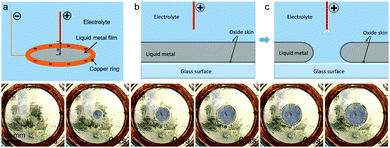
As shown in Fig. 1a, an insulated vessel is adopted to accommodate the galinstan film and electrolyte solution. The galinstan film was prepared on the vessel bottom in air. A thin layer of oxide was formed on the liquid metal surface as a result of oxidation. A copper ring cathode is placed in contact with the liquid metal film, while the other copper-wire anode is placed above the liquid metal at a certain distance in the surrounding electrolyte solution.
We now discuss the mechanism for the hole formation in the liquid metal. The whole liquid metal surface is fully covered by an oxide layer, including the interface regions between the vessel surface and the liquid metal. When a voltage is applied to the electrode tip, which is positioned above the liquid metal, the local oxide surface layer in both interface regions between the liquid metal and electrolyte as well as between the vessel surface and the liquid metal underneath the tip will be quickly reduced. The liquid metal has a very large surface tension and doesn’t wet the vessel surface.47 As a result, the exposed liquid metal deforms rapidly and curves inward at the interface because of the capillary effect. This process takes place in the center of the top surface of the liquid metal below the tip and spreads uniformly outward, creating a hole in the liquid metal film (see Fig. 1b and c). The hole size and the hole formation speed depend on the speed of the redox reaction, which is determined by the amplitude of the voltage on the tip, the tip distance, and the electrolyte concentration.
First, we investigated the effect of the voltage on the hole formation in the liquid metal using various voltages (v) of 0 to 18 V. In addition, different electrode spacings were investigated, since the distance (h) between the tip of the electrode wire and the liquid metal film directly affects the electrical field strength. We note the fact that an acid or a base solution can remove the oxide layer from the liquid metal film, causing the liquid metal to take on a spheroidal shape in the solution due to the high surface tension of the liquid metal.48,49 Therefore, we adopted a neutral solution (NaCl) for all our experiments. We have investigated the effects of short pulses or continuous voltage, the electrode distance, and the solution concentration on the voltage-induced non-contact electrochemical lithography effect.
We demonstrate the results for the smallest and the largest sizes of the holes that are formed and their spreading speeds under different conditions. We have observed the following main results: (1) a threshold voltage is needed to form a hole in the liquid metal. (2) The speed of the hole formation (rf) as well as the maximum size of the hole (R) is proportional to the applied voltage and the NaCl concentration for a fixed distance h, and they are inversely proportional to h. Here, the speed of the hole formation, rf, is defined as the rate of increase of the hole's diameter in mm per second. (3) The hole formation is irreversible. Snapshots for the hole formation process for v = 12 V are shown in Fig. 1d.
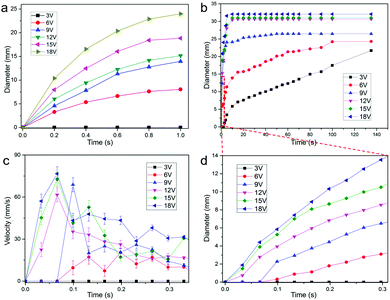
Fig. 2a illustrates the evolution of the hole formation in the liquid metal film by a short pulse of 12 V DC voltage, obtained by quickly switching the power supply on and off, with h = 1 mm in 0.01 mol L−1 NaCl. According to our observations, as soon as the voltage is applied, a hole is instantly formed and quickly spreads with a uniform omnidirectional speed, and the formation stops immediately once the applied voltage is removed. The diameters of the holes as a function of time (t) for different pulse voltages are shown in Fig. 2a. The final hole sizes increase monotonically with the applied pulsed voltages. The threshold voltage for hole-formation is 6 V. For v = 12 V, the hole size is about 9.5 mm at t = 0.4 s, and it becomes 15.2 mm after t = 1 s. The hole size can reach 25 mm for v = 18 V and t = 1 s (Fig. 1d).
Fig. 2b illustrates the evolution of the hole formation by a continuous applied DC voltage with h = 1 mm in 0.01 mol L−1 NaCl. The final diameter of the hole is proportional to the amplitude of the applied voltage. In the case of high voltages (v > 6 V), as soon as the continuous voltage is applied, a hole is instantly formed in the liquid metal, and it quickly reaches its final size in less than 5 s and then remains unchanged with time, even when the voltage is switched off. For low voltages (v = 3 and 6 V), the hole size increases quickly with time (for t < 10 s), then grows linearly for t > 20 s. For v = 3 and 6 V, the hole size increases to 7.6 and 15.7 mm at 20 s, respectively, then linearly increases up to 21.7 and 24.3 mm at the speed of 0.12 and 0.07 mm s−1, respectively, up to 140 s. For high voltages of 9–18 V, the hole size quickly increases and reaches its final size of 25.3, 30.7, 31.2, and 32.1 mm, respectively in less than 20 s. Snapshots of hole evolution for a continuous voltage of 12 V are presented in Fig. S1 in the ESI.†
The hole formation speed is an important parameter for potential applications of liquid metal electrochemical lithography, as shown in Fig. 2c. It is observed that the speeds, rf, are greater than 60 mm s−1 for t < 0.1 s when v > 12 V. The speeds decrease to 15–40 mm s−1 for t > 0.2 s and v > 6 V. The speeds drop to zero for t > 5 s and v > 12 V, t > 50 s and v = 9 V, and t > 100 s and v = 6 V, respectively (see Fig. 2b).
Fig. 2d shows the hole diameter vs. time within the first 0.3 s under various continuous voltages. For v > 3 V, the hole sizes increase with time. For v = 3 V, no hole is formed until t > 3 s. Interestingly, for v = 6 V, we observed that the hole size increases from 0.7 mm for t = 0.1 s to 3.1 mm for t = 0.3 s.
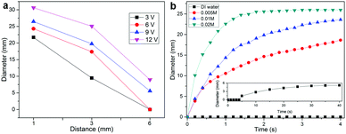
We also investigated the irreversible hole formation under different tip distances h. The experiments were conducted for several typical distances (h = 1, 3, and 6 mm) for a fixed solution of 0.01 mol L−1 NaCl. We observed that the larger the h is, the smaller the hole size will be (Fig. 3a). The final diameter of the holes for v = 3, 6, 9, and 12 V and h = 1 mm is reduced to 21.7, 24.3, 26.5, and 30.6 mm, respectively, and further decreases to 9.5, 17.4, 19.7 and 25.1 mm for the tip distance h = 3 mm. We note that no holes can be formed when h ≥ 6 mm and v < 6 V. This indicates that the electric field strength (E = V/h) generated between the tip and liquid metal surface is too weak to create a hole.
The hole formation was further examined using different solution concentrations for a fixed h = 1 mm and a fixed voltage of 9 V (Fig. 3b). The hole sizes increase with the concentration. For t = 1 s, the hole sizes are 0, 10.6, 12.3, and 22.6 mm for t = 1 s, and they increase to 5.2, 18.6, 23.0, and 25.9 mm for t = 4 s for the solution concentrations of 0 (deionized water), 0.005, 0.01, and 0.02 mol L−1, respectively. We found that the higher the solution concentration is, the quicker the holes will reach their final maximum sizes.
We briefly summarize the effects of the applied voltage, the tip distance, and the solution concentration on the hole formation process: a threshold voltage is required to form a hole in the liquid metal; the hole formation speed and the final size are proportional to the voltage and the NaCl concentration; and they are inversely proportional to the tip distance.
The irreversible hole formation that we have observed offers us a novel approach to non-contact electrochemical lithography for liquid metals. It affords great versatility in the hole formation approach to patterns in surface engineering of liquid metals. To demonstrate applications of the non-contact patterning process for liquid metals, we carried out experiments with continuous and pulsed voltages. Three patterning methods were demonstrated, which are the electrochemical dot matrix printing method, the electrochemical “writing” method, and the electrochemical movable type printing method. It is noteworthy that all these methods are non-contact.
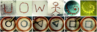
Fig. 4a presents examples of different patterns achieved using a single electrode tip, consisting of a Cu wire on top of the liquid metal film, and a 2 V constant voltage, with a 0.01 mol L−1 NaCl solution. The copper wire was put into the solution and slowly brought close to the liquid metal surface. After reaching a certain distance, a hole or a dot is formed in the liquid metal, and then the copper wire tip was retracted immediately to avoid further expansion of the hole. Each hole/dot formed in the liquid metal was about 2 mm in diameter. By purposefully arranging the hole/dot positions we can form any patterns that we choose. Patterns in the form of ‘U’, ‘O’, ‘W’, and a stick-figure were produced using the dot matrix method, as shown in Fig. 4a.
Furthermore, in our new approach, we can also use a pulsed voltage to implement a dot matrix approach to patterning. This method mimics the laser engraving method. It is well known that, for laser engraving, a laser beam is directed to draw a 2D vector, which evaporates the surface material dot by dot, forming any desired pattern on a solid surface. A ‘Crop Circle’ pattern was produced by this discontinuous electrochemical dot matrix approach (Fig. 4b).
In addition to the above described electrochemical dot matrix patterning process, a continuous electrochemical “writing” method with a constant voltage was employed. The electrode tip distance to the liquid metal surface and the applied voltage remain unchanged during the patterning process. Fig. S1 (ESI†) shows the “UOW” logo formed by using a continuous writing method.
We now demonstrate the third new electro-chemical patterning method for a liquid metal, which is movable type printing. The principle for this method is that the pattern of the electrode determines the pattern of the liquid metal. Conductive polymer (CP) electrodes in the shapes of a circle, triangle, and square were fabricated by using a 3D printer. These CP electrodes with geometric shapes were immersed in the solution and placed close to the liquid metal surface. As soon as a pulsed voltage is applied, a pattern that is the same as the geometric shape of the CP electrode is formed very quickly in the liquid metal. We also found that the sizes of the patterns are almost the same as for the CP electrodes. Fig. 4c–e shows the patterning process with and without an applied voltage. The corresponding videos can be found in the ESI.† The above demonstrated new electrochemical patterning methods are unique for liquid metal patterning. They are non-contact, maskless, and incur no loss of materials.
We summarize the applicable conditions of the method as follows. (1) The higher the voltage and solution concentration, the larger the hole size and the higher the formation speed. (2) The closer the tip is placed to the liquid metal film, the larger the hole size will be. (3) The higher the conductivity of the anode wire, the faster the formation speed. According to our observations, patterning performance would be influenced when the anode tip is close to the rim of the copper ring (less than 2 mm). However, when using a low conductive anode wire, the hole creation process would not affect the neighbouring patterns. So, a low conductivity anode is beneficial for patterning multiple crosses or complex patterns. Future studies should be aimed at creating micron size resolution patterns by reducing the thickness of the liquid metal film using low conductivity anode thin wires, and tuning other experiment conditions such as voltages, distances and solution concentrations.
Conclusions
In summary, a non-contact, maskless electrochemical lithography technique was developed for liquid metal at room temperature. The ability to form a hole in a liquid metal is the most important step in creating any pattern on it. We have investigated the effects of the voltage, the tip distance to the liquid metal surface in a solution, and the electrolyte concentration on the hole formation process for liquid metal. The hole sizes can be formed in the range from submillimeters to above 30 mm with the highest formation speed above 76 mm s−1 for high voltages and concentrations. Various patterns have been fabricated using three different approaches: electrochemical dot matrix printing, “writing”, and movable type printing.Conflicts of interest
There are no conflicts to declare.Acknowledgements
The authors thank Dr Tania Silver for critical reading of the manuscript. This work was partially supported by funding from the Australian Research Council through an ARC Future Fellowship (FT130100778) and a Discovery project (DP130102956).Notes and references
- J. Y. Zhu, S.-Y. Tang, K. Khoshmanesh and K. Ghorbani, ACS Appl. Mater. Interfaces, 2016, 8, 2173–2180 CAS.
- A. Zavabeti, T. Daeneke, A. F. Chrimes, A. P. O’Mullane, J. Zhen Ou, A. Mitchell, K. Khoshmanesh and K. Kalantar-zadeh, Nat. Commun., 2016, 7, 12402 CrossRef CAS PubMed.
- X. Wang and J. Liu, Micromachines, 2016, 7, 206 CrossRef.
- D. Morales, N. A. Stoute, Z. Yu, D. E. Aspnes and M. D. Dickey, Appl. Phys. Lett., 2016, 109, 091905 CrossRef.
- Y. Lu, Q. Hu, Y. Lin, D. B. Pacardo, C. Wang, W. Sun, F. S. Ligler, M. D. Dickey and Z. Gu, Nat. Commun., 2015, 6, 10066 CrossRef CAS PubMed.
- R. C. Chiechi, E. A. Weiss, M. D. Dickey and G. M. Whitesides, Angew. Chem., 2008, 120, 148–150 CrossRef.
- Y. Chen, Z. Liu, D. Zhu, S. Handschuh-Wang, S. Liang, J. Yang, T. Kong, X. Zhou, Y. Liu and X. Zhou, Mater. Horiz., 2017, 4, 591–597 RSC.
- S. A. Chechetka, Y. Yu, X. Zhen, M. Pramanik, K. Pu and E. Miyako, Nat. Commun., 2017, 8, 15432 CrossRef CAS PubMed.
- Y. Yu and E. Miyako, Angew. Chem., 2017, 129, 13794–13799 CrossRef.
- L. Sheng, J. Zhang and J. Liu, Adv. Mater., 2014, 26, 6036–6042 CrossRef CAS PubMed.
- M. R. Khan, C. B. Eaker, E. F. Bowden and M. D. Dickey, Proc. Natl. Acad. Sci. U. S. A., 2014, 111, 14047–14051 CrossRef CAS PubMed.
- S.-Y. Tang, K. Khoshmanesh, V. Sivan, P. Petersen, A. P. O’Mullane, D. Abbott, A. Mitchell and K. Kalantar-zadeh, Proc. Natl. Acad. Sci. U. S. A., 2014, 111, 3304–3309 CrossRef CAS PubMed.
- Z. Yu, Y. Chen, F. F. Yun and X. Wang, Adv. Eng. Mater., 2017, 19, 1700190 CrossRef.
- M. Li, Y. Su, H. Zhang and B. Dong, Nano Res., 2017 DOI:10.1007/s12274-017-1799-5.
- M. Wang, C. Trlica, M. R. Khan, M. D. Dickey and J. J. Adams, J. Appl. Phys., 2015, 117, 194901 CrossRef.
- J. H. So, J. Thelen, A. Qusba, G. J. Hayes, G. Lazzi and M. D. Dickey, Adv. Funct. Mater., 2009, 19, 3632–3637 CrossRef CAS.
- M. Kubo, X. Li, C. Kim, M. Hashimoto, B. J. Wiley, D. Ham and G. M. Whitesides, Adv. Mater., 2010, 22, 2749–2752 CrossRef CAS PubMed.
- Y. Lin, C. Cooper, M. Wang, J. J. Adams, J. Genzer and M. D. Dickey, Small, 2015, 11, 6397–6403 CrossRef CAS PubMed.
- E. Palleau, S. Reece, S. C. Desai, M. E. Smith and M. D. Dickey, Adv. Mater., 2013, 25, 1589 CrossRef CAS PubMed.
- D. P. Parekh, C. Ladd, L. Panich, K. Moussa and M. D. Dickey, Lab Chip, 2016, 16, 1812–1820 RSC.
- J. Jeon, J.-B. Lee, S. K. Chung and D. Kim, Lab Chip, 2017, 17, 128–133 RSC.
- K. Khoshmanesh, S.-Y. Tang, J. Y. Zhu, S. Schaefer, A. Mitchell, K. Kalantar-zadeh and M. D. Dickey, Lab Chip, 2017, 17, 974–993 RSC.
- J. Yang, T. Zhou, L. Zhang, D. Zhu, S. Handschuh-Wang, Z. Liu, T. Kong, Y. Liu, J. Zhang and X. Zhou, J. Mater. Chem. C, 2017, 5, 6790–6797 RSC.
- S. Bauer, S. Bauer-Gogonea, I. Graz, M. Kaltenbrunner, C. Keplinger and R. Schwödiauer, Adv. Mater., 2014, 26, 149–162 CrossRef CAS PubMed.
- J. Xu, Sci. Bull., 2015, 60, 1047–1048 CrossRef.
- J. Liu, Sci. China: Technol. Sci., 2016, 59, 1793–1794 CrossRef.
- L. Hines, K. Petersen, G. Z. Lum and M. Sitti, Adv. Mater., 2017, 29, 1603483 CrossRef PubMed.
- Y. Liu, M. Gao, S. Mei, Y. Han and J. Liu, Appl. Phys. Lett., 2013, 103, 064101 CrossRef.
- W. F. Reus, M. M. Thuo, N. D. Shapiro, C. A. Nijhuis and G. M. Whitesides, ACS Nano, 2012, 6, 4806–4822 CrossRef CAS PubMed.
- W. Liu, Z. Chen, G. Zhou, Y. Sun, H. R. Lee, C. Liu, H. Yao, Z. Bao and Y. Cui, Adv. Mater., 2016, 28, 3578–3583 CrossRef CAS PubMed.
- B. Dong, D. Y. Zhong, L. F. Chi and H. Fuchs, Adv. Mater., 2005, 17, 2736–2741 CrossRef CAS.
- M. Varga, C. Ladd, S. Ma, J. Holbery and G. Troster, Lab Chip, 2017, 17, 3272–3278 RSC.
- J. W. Boley, E. L. White, G. T. C. Chiu and R. K. Kramer, Adv. Funct. Mater., 2014, 24, 3501–3507 CrossRef CAS.
- D. J. Lipomi, Adv. Mater., 2015, 28, 4180–4183 CrossRef PubMed.
- M. C. LeMieux and Z. Bao, Nat. Nanotechnol., 2008, 3, 585–586 CrossRef CAS PubMed.
- M. D. Dickey, Adv. Mater., 2017, 29, 1606425 CrossRef PubMed.
- Y. Zhang, Y. Hu, P. Zhu, F. Han, Y. Zhu, R. Sun and C.-P. Wong, ACS Appl. Mater. Interfaces, 2017, 9, 35968–35976 CAS.
- L. Ren, J. Zhuang, G. Casillas, H. Feng, Y. Liu, X. Xu, Y. Liu, J. Chen, Y. Du, L. Jiang and S. X. Dou, Adv. Funct. Mater., 2016, 26, 8111–8118 CrossRef CAS.
- R. K. Kramer, C. Majidi and R. J. Wood, Adv. Funct. Mater., 2013, 23, 5292–5296 CrossRef CAS.
- T. Lu, L. Finkenauer, J. Wissman and C. Majidi, Adv. Funct. Mater., 2014, 24, 3351–3356 CrossRef CAS.
- Y. Zheng, Z.-Z. He, J. Yang and J. Liu, Sci. Rep., 2014, 4, 4588 CrossRef PubMed.
- M. J. Madou, Fundamentals of Microfabrication and Nanotechnology, CRC, 3rd edn, 2012 Search PubMed.
- M. D. Dickey, R. C. Chiechi, R. J. Larsen, E. A. Weiss, D. A. Weitz and G. M. Whitesides, Adv. Funct. Mater., 2008, 18, 1097–1104 CrossRef CAS.
- C. Ladd, J.-H. So, J. Muth and M. D. Dickey, Adv. Mater., 2013, 25, 5081–5085 CrossRef CAS PubMed.
- L. Wang and J. Liu, Sci. China: Technol. Sci., 2014, 57, 1721–1728 CrossRef CAS.
- M. R. Khan, J. Bell and M. D. Dickey, Adv. Mater. Interfaces, 2016, 3, 1600546 CrossRef.
- T. Liu, P. Sen and C.-J. C. Kim, J. Microelectromech. Syst., 2012, 21, 443–450 CrossRef CAS.
- R. K. Kramer, J. W. Boley, H. A. Stone, J. C. Weaver and R. J. Wood, Langmuir, 2014, 30, 533–539 CrossRef CAS PubMed.
- K. Doudrick, S. Liu, E. M. Mutunga, K. L. Klein, V. Damle, K. K. Varanasi and K. Rykaczewski, Langmuir, 2014, 30, 6867–6877 CrossRef CAS PubMed.
Footnote |
| † Electronic supplementary information (ESI) available: Experimental details and snapshots. See DOI: 10.1039/c7mh00819h |
| This journal is © The Royal Society of Chemistry 2018 |


