
 Open Access Article
 This Open Access Article is licensed under a Creative Commons Attribution-Non Commercial 3.0 Unported Licence
Structural and electronic properties of hydrogenated GaBi and InBi honeycomb monolayers with point defects
Yunzhen Zhang,
Han Ye *,
Zhongyuan Yu*,
Han Gao and
Yumin Liu
*,
Zhongyuan Yu*,
Han Gao and
Yumin Liu
State Key Laboratory of Information Photonics and Optical Communications, Beijing University of Posts and Telecommunications, Beijing 100876, China. E-mail: Han_ye@bupt.edu.cn; Yuzhongyuan30@hotmail.com
First published on 13th February 2018
Abstract
First-principles calculations are carried out to systematically investigate the structural and electronic properties of point defects in hydrogenated GaBi and InBi monolayers, including vacancies, antisites and Stone–Wales (SW) defects. Our results imply that the perfect H2-Ga(In)Bi is a semiconductor with a bandgap of 0.241 eV (0.265 eV) at the Γ point. The system turns into a metal by introducing a Ga(In) vacancy, substituting a Bi with a Ga(In) atom or substituting an In with a Bi atom. Other defect configurations can tune the bandgap value in the range from 0.09 eV to 0.3 eV. In particular, the exchange of neighboring Ga(In) and Bi increases the bandgap, meanwhile the spin splitting effect is preserved. All SW defects decrease the bandgap. The lowest formation energy of defects occurs when substituting a Ga(In) with a Bi atom and the values of SW defects vary from 0.98 eV to 1.77 eV.
1 Introduction
Topological insulators (TIs) have captured unprecedented scientific and technological interests in the past few years.1–5 Two-dimensional (2D) TIs, known as quantum spin Hall (QSH) insulators, provide small bandgap edge states with the protection of time-reversal symmetry, which ensures the propagation direction of electrons on the surface locked to their spin orientation.6–8 However, due to the small bandgaps, group IV 2D materials such as graphene,9 silicene and germanene,10–12 operate impracticably at room temperature. Recently, potential QSH insulator materials with large bandgaps were found to be promising building blocks for novel coherent spin transport related devices.13–15The binary compounds of group III elements and bismuth with buckled honeycomb structure have been studied and predicted to have large bandgaps due to the large spin–orbit coupling (SOC) effect of Bi atoms, which is desirable for room-temperature spintronic applications. Among these 2D sheets, only GaBi, InBi and TlBi exhibit nontrivial topological characteristics.16 However, imaginary frequency modes were observed in the phonon spectrum of their pristine structures. It has been found that low buckled structure and passivation including halogenation, hydrogenation and methyl-functionalization stabilize the structure and increase the bandgap.17–26 Especially, the hydrogen bonds can also simulate the electronic structure with the effect of a substrate and efficiently identify the quantum spin Hall phase of these 2D materials.17,35,36 Moreover, functionalized III-Bi monolayers can realize nontrivial topological states preferably compared with the pristine structures.17,22,26
Generally, the electronic properties of materials are influenced by the defects which are mainly introduced during the growth process and considered as an adverse factor. But it is worth mentioning that sometimes defects can bring beneficial effects which make the materials suitable for other applications.27,28 Typical point defects have been observed and investigated in graphene, silicene, hexagonal GeC, group III nitride monolayers, etc.29–31 The imperfections make it possible to tailor the electronic properties,32–34 for example, the bandgap which is crucial for spintronic applications. To the best of our knowledge, systematic investigations of imperfections in 2D group III bismide honeycombs have not been reported. In this paper, we explore the impacts of the possible point defects in H2-GaBi and H2-InBi monolayers on the structural and electronic properties. Nine defect configurations including vacancies, antisites and Stone–Wales (SW) defects are considered.
2 Computational methods and models
Based on density-functional theory (DFT) method, first-principles calculations of geometry optimization and electronic properties are implemented in the Vienna ab initio simulation package (VASP).37,38 The projector augmented wave (PAW) pseudopotentials are chosen to describe the actual electron-ion potential and the exchange-correlation functions are set as the Perdew–Burke–Ernzerhof (PBE) form of the generalized gradient approximation (GGA).39–42 After convergence test, the maximum kinetic energy cut-off of the plane wave basis set is chosen as 400 eV. Using the Quasi-Newton method, the optimization of atomic positions and lattice constants are carried out until the maximum Hellmann–Feynman force on each atom becomes less than 0.01 eV/Å. The energy convergence criterion of self-consistent calculations is set less than 10−5 eV between two continuous steps. A vacuum layer of 20 Å is built to avoid periodic interactions. Based on Monkhorst–Pack scheme,43 the k-point samplings for Brillouin zone integration of 4 × 4 and 6 × 6 supercells are set 7 × 7 × 1 and 4 × 4 × 1, respectively. Besides, the SOC effect is included in all self-consistent electronic structure calculations.44With regard to all the structures of group III bismide monolayers, the binding energy per atom is defined as
 | (1) |
| Eform = EP − Etotal + μSub − μAdd | (2) |
To investigate the impacts of defects in H2-Ga(In)Bi monolayers on the electronic structure, a series of point defects including vacancies, antisites and SW defects are modeled. To avoid the interaction between two isolated defects, a 4 × 4 supercell is employed to simulate the vacancies and antisites while a 6 × 6 supercell is used for the SW defects. The abbreviations of nine defects are presented as below:
(a) Vacancies: structure with one subtracted Bi(Ga, In) atom is labelled as VBi(Ga,In); structure with one pair of subtracted Ga(In)–Bi atoms is labelled as VGa(In)Bi.
(b) Antisites: structure with exchanged neighboring Ga(In) and Bi atom is labelled as Ga(In)↔Bi; substituting a Ga(In) atom with a Bi atom and substituting a Bi atom with a Ga(In) atom are labelled as BiGa(In) and Ga(In)Bi, respectively.
(c) Stone–Wales: structure with an in-plane 90° rotation of one Ga(In)–Bi bond is labelled as SW-IP; structure with an out-of-plane 90° rotation of one Ga(In)–Bi bond is labelled as SW-OP.
3 Results and discussion
3.1 Perfect hydrogenated honeycomb monolayer
We first consider the perfect hydrogenated GaBi and InBi monolayers as demonstrated in Fig. 1(a). The hydrogens cover the monolayer on both sides and its number is equal to the number of III, V atoms in the supercell. After full relaxation, both group III bismide monolayers remain typical buckled honeycomb structure. The optimized lattice constants of H2-GaBi, H2-InBi 4 × 4 supercells are 4.580 Å and 4.881 Å, respectively. Electronic structures including SOC effects shown in Fig. 1(b) indicate that the perfect monolayers are TIs with large bandgaps opened at Γ point, whose values are 0.241 eV and 0.265 eV for GaBi and InBi, respectively. Our results are in satisfactory agreement with previous DFT calculations.18 The valence band maximum (VBM) of these two systems locate slightly off the Γ point, resulted from the spin splitting. Moreover, the s-orbital electrons turn to occupy the valence band with the SOC effect. The band order gets inverted near the Fermi-level and the band near VBM is s-orbital dominated by 64%.17,20 Other structural and electronic parameters are listed in Table 1.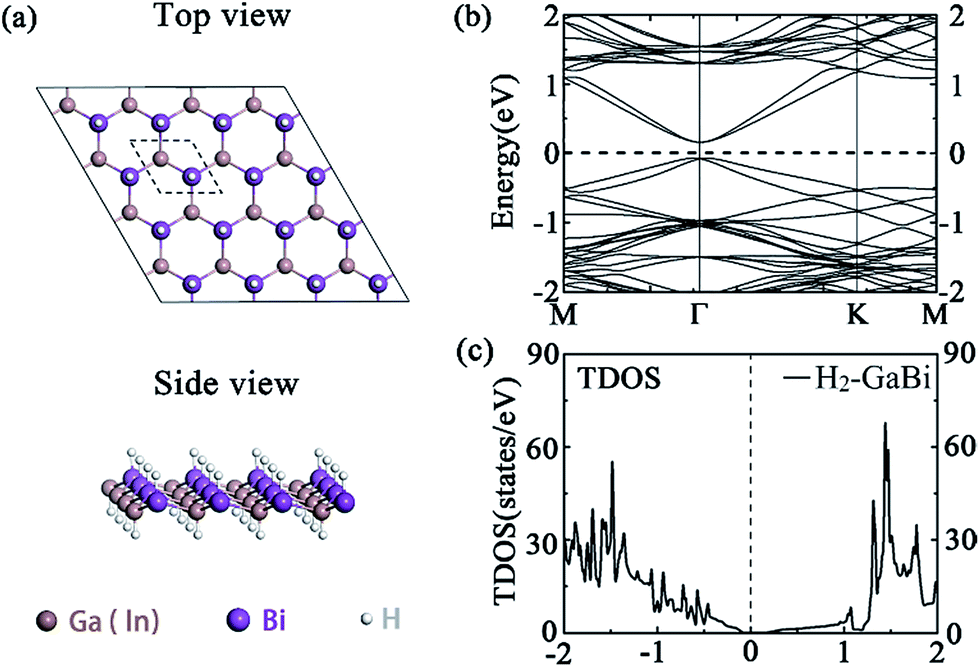 | ||
| Fig. 1 (a) The top and side view of (4 × 4) supercell of perfect H2-GaBi monolayer, (b) band structures of H2-GaBi, (c) total density of states (TDOS) of H2-GaBi. The Fermi energy is set to zero. | ||
| System | Our calculation | Ref. 18 | ||
|---|---|---|---|---|
| H2-GaBi | H2-InBi | H2-GaBi | H2-InBi | |
| a (Å) | 4.580 | 4.881 | 4.588 | 4.891 |
| Δ (Å) | 0.798 | 0.853 | 0.795 | 0.851 |
| d (Å) | 2.762 | 2.944 | — | — |
| Eb (eV) | 3.256 | 3.118 | — | — |
| Egap (eV) | 0.241 | 0.265 | 0.241 | 0.270 |
3.2 Vacancy defects
The structures of hydrogenated GaBi monolayer with vacancies are demonstrated in Fig. 2. After geometry optimization, the lattice constant of all structures have a slight reduction compared with the perfect H2-GaBi. By removing one bismuth atom in GaBi monolayer, the shift of atom position around defect can be easily observed. The VBi defect introduces several vacancy states and shifts the conduction band minimum (CBM) away from the Γ point, leading the system to be a nonmagnetic indirect semiconductor with a bandgap of 0.19 eV. Unlikely, by removing one gallium atom in the monolayer, the Fermi-level of VGa system shifts down about 0.56 eV and the system becomes metallic as illustrated in Fig. 2(b). The partial density of states (PDOS) shows that the main contribution near the Fermi-level comes from p-orbital of bismuth atoms. In the case of VGaBi defect, one octagon and two pentagons are formed by subtracting a GaBi pair. The defect shifts the CBM and the system occurs to be an indirect semiconductor with a bandgap of 0.15 eV. As listed in Table 2, the formation energies of VBi, VGa and VGaBi systems are 1.91 eV, 0.47 eV and 1.47 eV respectively, indicating relatively low energy barrier between the perfect H2-GaBi monolayer and the vacancy of Ga atom. We also calculate the vacancies in H2-InBi monolayer and obtain a series of similar results from the data.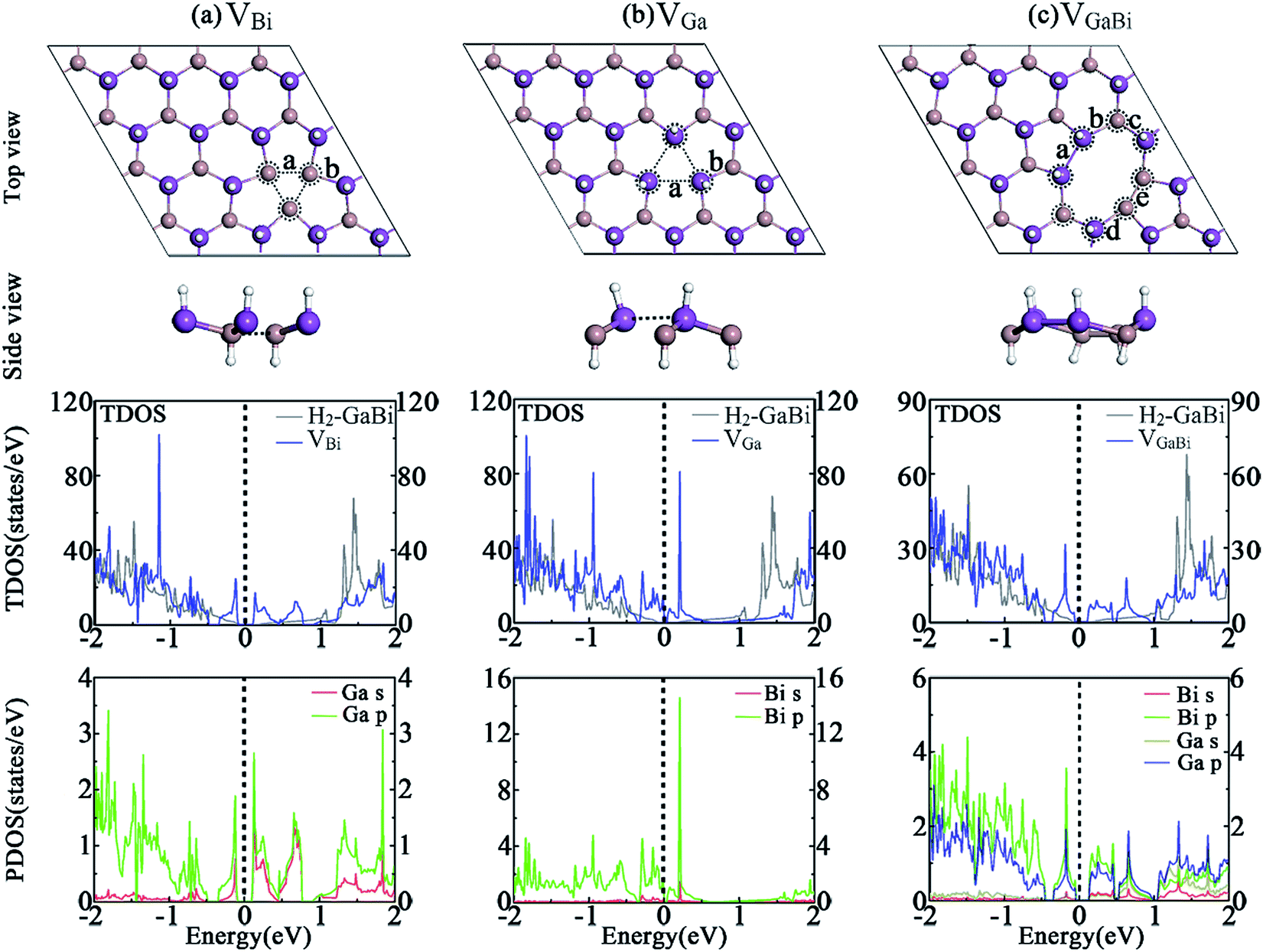 | ||
| Fig. 2 Optimized geometries of H2-GaBi with vacancy defects in 4 × 4 supercells are represented in (a) VBi, (b) VGa and (c) VGaBi. The TDOS of whole system and the PDOS of atoms circled by dotted lines are shown below the corresponding structure. The Fermi-level is set to zero. | ||
| System | GaBi | InBi | ||||
|---|---|---|---|---|---|---|
| Defects | VBi | VGa | VGaBi | VBi | VIn | VInBi |
| Eb (eV per atom) | 3.214 | 3.252 | 3.119 | 3.076 | 3.118 | 2.987 |
| Eform (eV) | 1.91 | 0.47 | 1.47 | 1.55 | 0.30 | 1.15 |
| Egap (eV) | 0.19 | M | 0.15 | 0.21 | M | 0.19 |
| l (Å) | 17.89 | 18.08 | 18.17 | 19.11 | 19.17 | 19.34 |
| d (Å) | a = 3.06, b = 2.88 | a = 3.89, b = 2.78 | a = 3.26, b = 3.06, c = 2.75, d = 3.00, e = 2.60 | a = 3.41, b = 3.04 | a = 3.96, b = 2.95 | a = 3.22, b = 3.50, c = 2.92, d = 3.18, e = 2.93 |
3.3 Antisite defects
Fig. 3 presents the structures of hydrogenated GaBi monolayer with antisite defects. After geometry optimization, The GaBi and Ga↔Bi systems remain normally buckled honeycomb structure, while the bismuth cluster in BiGa system turns to be an inversely buckled honeycomb structure. The band structure indicates that, by substituting gallium atom with bismuth in BiGa antisite, no spin splitting appears at the valence band which makes the system to be a direct semiconductor with a bandgap of 0.2 eV. In Fig. 3(a), the TDOS demonstrates that the states of conduction band rise smoothly as the energy increases, which is similar to the perfect H2-GaBi. The valence band is isolated from other bands below the Fermi-level, resulting from the bismuth cluster around the antisite defect. The PDOS of bismuth cluster reveals the fact that most states locate near the VBM. Similar to the VGa system, the Fermi-level of GaBi shifts down about 0.37 eV, leading the system to be metallic as shown in Fig. 3(b), while the band order is similar to the perfect H2-GaBi near the Dirac cone. In the case of Ga↔Bi defect in Fig. 3(c), the bandgap increases to about 0.29 eV at Γ point, meanwhile the spin splitting effect is preserved. When substituting indium atom with bismuth atom, the defect leads the system to be metallic, which can be considered as the result of the structure. The atoms around antisite defect BiIn do not turn to the distinct inversely buckled honeycomb like the BiGa system, so that the bismuth atoms make a different change to the band structure near the Fermi-level, leading the valence band to shift up at high symmetry point K. The binding energy and formation energy results also indicate that BiIn system is more stable.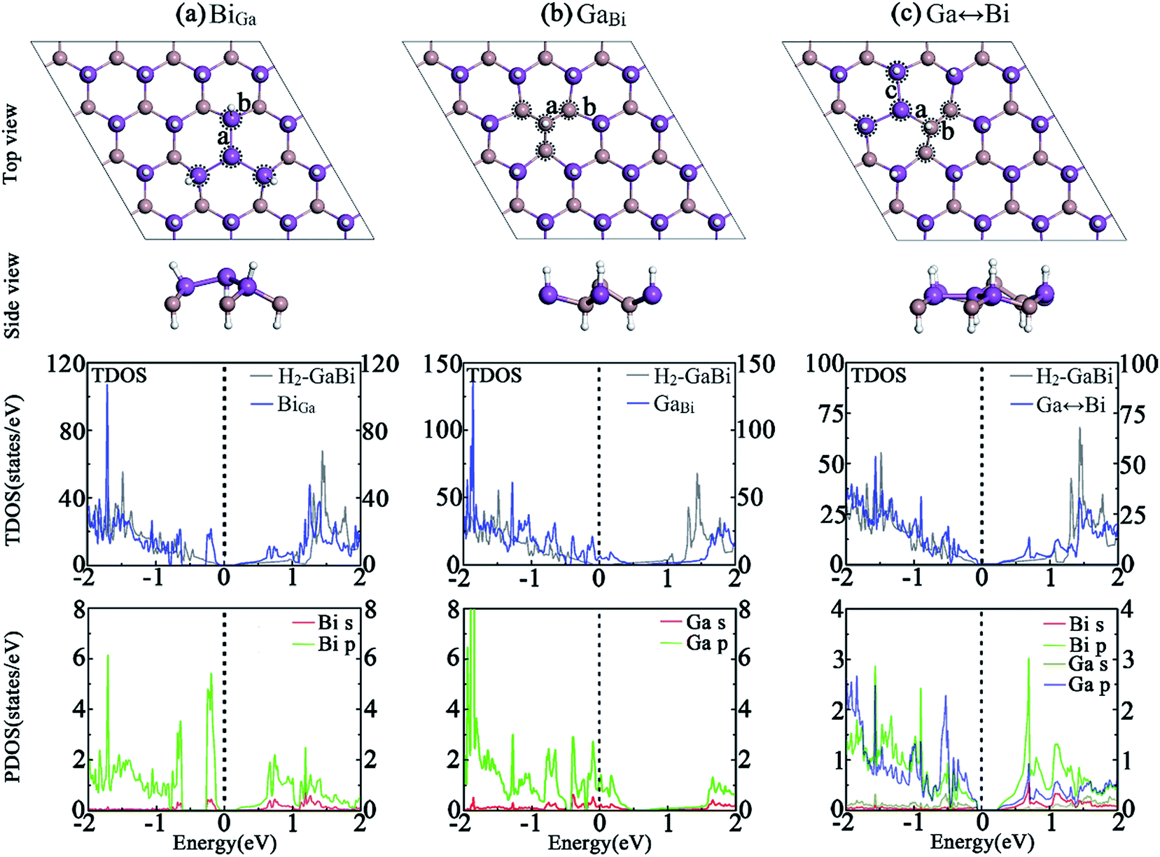 | ||
| Fig. 3 Optimized geometries of H2-GaBi with antisite defects in 4 × 4 supercells are represented in (a) BiGa, (b) GaBi and (c) Ga↔Bi. The TDOS of whole system and the PDOS of atoms circled by dotted lines are shown below the corresponding structure. The Fermi-level is set to zero. | ||
Table 3 show that the lattice constants decrease when replacing big atom with small atom and vise versa. The lattice of Ga↔Bi becomes smaller while the In↔Bi becomes larger. The formation energies of BiGa, GaBi and Ga↔Bi systems are 0.25 eV, 1.27 eV and 0.39 eV, respectively. It is expected easier to replace a gallium or indium atom with bismuth atom and exchange neighboring atoms, compared with subtracting a bismuth atom from the lattice. Together with vacancies, the results imply that VGa(In), BiGa(In) and Ga(In)↔Bi may be the dominant defects during the fabrication of H2-Ga(In)Bi monolayer.
| System | GaBi | InBi | ||||
|---|---|---|---|---|---|---|
| Defects | BiGa | GaBi | Ga↔Bi | BiIn | InBi | In↔Bi |
| Eb (eV per atom) | 3.268 | 3.222 | 3.250 | 3.138 | 3.072 | 3.109 |
| Eform (eV) | 0.25 | 1.27 | 0.39 | −0.007 | 1.62 | 0.58 |
| Egap (eV) | 0.20 | M | 0.29 | M | M | 0.30 |
| l (Å) | 18.41 | 18.08 | 18.32 | 19.71 | 19.40 | 19.60 |
| d (Å) | a = 3.14, b = 2.76 | a = 2.53, b = 2.84 | a = 2.93, b = 2.47, c = 3.06 | a = 3.14, b = 2.95 | a = 2.91, b = 3.00 | a = 3.14, b = 2.80, c = 3.07 |
3.4 Stone–Wales defects
Besides vacancy and antisite defects, Stone–Wales defect is regarded as an important type of defect in 2D materials,45–48 such as graphene, germanium carbide and other similar honeycomb structures. The SW defect is formed by rotating a pair of two atoms by 90 degrees with respect to the midpoint of their bond, which does not require adding or subtracting atoms. The formation energy is usually around several electron volts which is fairly high. The rearrangement of the atoms is thought to introduce significant influences to the chemical, electrical, and mechanical properties. An in-plane 90° rotation of Ga–Bi bond involves two directions, the clockwise and anti-clockwise, and leads to the same structure and lattice parameters after optimization. Due to the buckled structure, the out-of-plane rotation forms two distinct SW defects by different rotation directions. Here, we build 6 × 6 perfect H2-GaBi and H2-InBi supercells to simulate the isolated SW defect and relax the systems to reach stress equilibrium. The optimized structures are demonstrated in Fig. 4. For SW-IP defect, the rotated Ga-Bi bond results in the breaking of original hexagons and the formation of pentagons and heptagons. Regarding the SW-OP defects, the top views of the OP1 and OP2 look similar to the H2-GaBi and Ga↔Bi structure, respectively, but the positions of the gallium and bismuth atoms are different. The heights of the rotated Ga and Bi atoms exhibit a reversal meanwhile the formation of inversed buckling leads the hydrogenation to occur on the opposite side.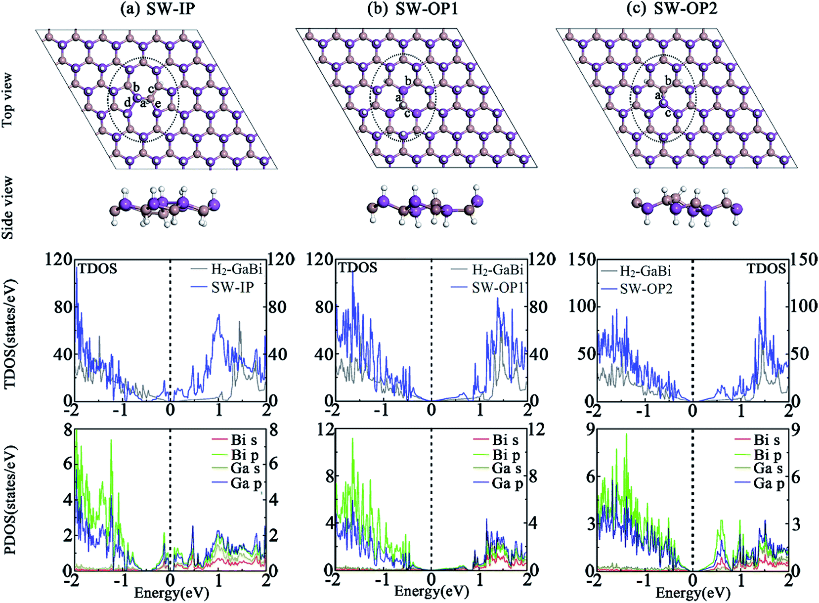 | ||
| Fig. 4 Optimized Structures of H2-GaBi with SW defects in 6 × 6 supercells are represented in (a) SW-IP, (b) SW-OP1 and (c) SW-OP2. The TDOS of whole system and the PDOS of atoms circled by dotted lines are shown below the corresponding structure. The Fermi-level is set to zero. | ||
The corresponding TDOS and PDOS of three systems with SW defects are demonstrated in Fig. 4. The band structures infer that the shape of Dirac cone at Γ point maintains in three systems. The TDOS results state that the SW defects produce appreciable effect to the electronic structures. As listed in Table 4, the bandgap at Γ point of H2-GaBi monolayer with SW-IP, SW-OP1 and SW-OP2 defects are 0.102 eV, 0.092 eV and 0.153 eV, respectively, indicating the downward trend of energy gap with the effect of SW defects. The formation energies of the three defects in H2-GaBi are 1.29 eV, 0.98 eV and 1.05 eV, respectively. The values fall within the similar range of vacancy and antisite defects, and lower than SW defects in other 2D materials such as GeC.49,50 The in-plane SW defect is shown arduous among the three configurations, suggesting the new pentagons and heptagons in GaBi are less stable than original hexagons.
| System | GaBi | InBi | ||||
|---|---|---|---|---|---|---|
| Defects | SW-IP | SW-OP1 | SW-OP2 | SW-IP | SW-OP1 | SW-OP2 |
| Eb (eV per atom) | 3.247 | 3.250 | 3.249 | 3.109 | 3.110 | 3.106 |
| Eform (eV) | 1.29 | 0.98 | 1.05 | 1.33 | 1.20 | 1.77 |
| Egap (eV) | 0.10 | 0.09 | 0.15 | 0.12 | 0.13 | 0.18 |
| l (Å) | 27.88 | 27.09 | 27.47 | 29.67 | 28.71 | 29.26 |
| d (Å) | a = 2.73, b = 2.80, c = 2.50, d = 3.10, e = 2.85 | a = 2.77, b = 2.78, c = 2.76 | a = 2.91, b = 2.48, c = 3.06 | a = 2.94, b = 3.01, c = 2.84, d = 3.09, e = 3.04 | a = 2.95, b = 2.95, c = 2.94 | a = 3.13, b = 2.80, c = 3.05 |
4 Conclusions
In summary, we present a first-principles study of the structural and electronic properties of nine point defects in hydrogenated GaBi and InBi monolayers. The results indicate the bandgap of monolayer can be tuned from 0 eV (metallic) to 0.3 eV by defect configurations. By removing one Ga(In) atom in the H2-Ga(In)Bi, the system turns to be metallic. The exchange of Ga(In) and Bi atoms, as one of antisite defects, enhances the bandgap meanwhile the spin splitting effect is preserved. In contrast, a decreasing bandgap is observed in monolayer by introducing SW defects. On the other hand, VGa(In), BiGa(In) and Ga(In)↔Bi have lower formation energy because the energy required to subtract a Bi atom from system is larger than to subtract a Ga(In) or add a Bi atom. The formation energies of SW defects in hydrogenated GaBi and InBi monolayer are comparable with vacancies and antisites. Our study shows the point defects in H2-Ga(In)Bi monolayers provide an approach to deliberately tailor the electronic properties, and the data are expected useful for future experimental synthesis and device design.Conflicts of interest
There are no conflicts to declare.Acknowledgements
This work was supported by the National Natural Science Foundation of China (Grants No. 61401035), the National Basic Research Program of China “973” (Grant No. 2014CB643901) and the Fund of State Key Laboratory of Information Photonics and Optical Communications (Beijing University of Posts and Telecommunications), P. R. China (IPOC2017ZT07).Notes and references
- A. Bansil, H. Lin and T. Das, Rev. Mod. Phys., 2016, 88, 21004 CrossRef.
- N. Nagaosa, J. Sinova, S. Onoda, A. H. MacDonald and N. P. Ong, Rev. Mod. Phys., 2010, 82, 1539 CrossRef.
- H. Weng, R. Yu, X. Hu, X. Dai and Z. Fang, Adv. Phys., 2015, 64, 227–282 CrossRef.
- B. Yan and S.-C. Zhang, Rep. Prog. Phys., 2012, 75, 96501 CrossRef PubMed.
- J. E. Moore, Nature, 2010, 464, 194–198 CrossRef CAS PubMed.
- M. Z. Hasan and C. L. Kane, Rev. Mod. Phys., 2010, 82, 3045 CrossRef CAS.
- X.-L. Qi and S.-C. Zhang, Rev. Mod. Phys., 2011, 83, 1057 CrossRef CAS.
- B. A. Bernevig and S.-C. Zhang, Phys. Rev. Lett., 2006, 96, 106802 CrossRef PubMed.
- C. L. Kane and E. J. Mele, Phys. Rev. Lett., 2005, 95, 226801 CrossRef CAS PubMed.
- C.-C. Liu, W. Feng and Y. Yao, Phys. Rev. Lett., 2011, 107, 76802 CrossRef PubMed.
- C.-C. Liu, H. Jiang and Y. Yao, Phys. Rev. B: Condens. Matter Mater. Phys., 2011, 84, 195430 CrossRef.
- W. Qiu, H. Ye, Z. Yu and Y. Liu, Superlattices Microstruct., 2016, 97, 250–257 CrossRef CAS.
- L. Fu, C. L. Kane and E. J. Mele, Phys. Rev. Lett., 2007, 98, 106803 CrossRef PubMed.
- L. Fu and C. L. Kane, Phys. Rev. Lett., 2009, 102, 216403 CrossRef PubMed.
- X.-L. Qi, T. L. Hughes and S.-C. Zhang, Phys. Rev. B: Condens. Matter Mater. Phys., 2008, 78, 195424 CrossRef.
- F.-C. Chuang, L.-Z. Yao, Z.-Q. Huang, Y.-T. Liu, C.-H. Hsu, T. Das, H. Lin and A. Bansil, Nano Lett., 2014, 14, 2505–2508 CrossRef CAS PubMed.
- C. P. Crisostomo, L.-Z. Yao, Z.-Q. Huang, C.-H. Hsu, F.-C. Chuang, H. Lin, M. A. Albao and A. Bansil, Nano Lett., 2015, 15, 6568–6574 CrossRef CAS PubMed.
- Y. Ma, Y. Dai, L. Kou, T. Frauenheim and T. Heine, Nano Lett., 2015, 15, 1083–1089 CrossRef CAS PubMed.
- S. Li, W. Ji, C. Zhang, S. Hu, P. Li, P. Wang, B. Zhang and C. Cao, Sci. Rep., 2016, 6, 23242 CrossRef CAS PubMed.
- Y. Kim, W. S. Yun and J. D. Lee, Sci. Rep., 2016, 6, 33395 CrossRef CAS PubMed.
- R. R. Q. Freitas, F. de Brito Mota, R. Rivelino, C. M. C. de Castilho, A. Kakanakova-Georgieva and G. K. Gueorguiev, Nanotechnology, 2016, 27, 55704 CrossRef CAS PubMed.
- Y. Ma, X. Li, L. Kou, B. Yan, C. Niu, Y. Dai and T. Heine, Phys. Rev. B: Condens. Matter Mater. Phys., 2015, 91, 235306 CrossRef.
- L. Li, X. Zhang, X. Chen and M. Zhao, Nano Lett., 2015, 15, 1296–1301 CrossRef CAS PubMed.
- S.-P. Chen, Z.-Q. Huang, C. P. Crisostomo, C.-H. Hsu, F.-C. Chuang, H. Lin and A. Bansil, Sci. Rep., 2016, 6, 31317 CrossRef CAS PubMed.
- R. R. Q. Freitas, F. de Brito Mota, R. Rivelino, C. M. C. De Castilho, A. Kakanakova-Georgieva and G. K. Gueorguiev, Phys. Rev. B: Condens. Matter Mater. Phys., 2015, 27, 485306 CrossRef CAS PubMed.
- R. R. Q. Freitas, R. Rivelino, F. de Brito Mota, C. M. C. de Castilho, A. Kakanakova-Georgieva and G. K. Gueorguiev, J. Phys. Chem. C, 2015, 119, 23599–23606 CAS.
- A. F. Kohan, G. Ceder, D. Morgan and C. G. Van de Walle, Phys. Rev. B: Condens. Matter Mater. Phys., 2000, 61, 15019 CrossRef CAS.
- Q. Xu, H. Schmidt, S. Zhou, K. Potzger, M. Helm, H. Hochmuth, M. Lorenz, A. Setzer, P. Esquinazi and C. Meinecke, Appl. Phys. Lett., 2008, 92, 82508 CrossRef.
- F. Banhart, J. Kotakoski and A. V. Krasheninnikov, ACS Nano, 2010, 5, 26–41 CrossRef PubMed.
- J. Gao, J. Zhang, H. Liu, Q. Zhang and J. Zhao, Nanoscale, 2013, 5, 9785–9792 RSC.
- H. Gao, H. Ye, Z. Yu, Y. Zhang, Y. Liu and Y. Li, Superlattices Microstruct., 2017, 112, 136–142 CrossRef CAS.
- J.-H. Chen, L. Li, W. G. Cullen, E. D. Williams and M. S. Fuhrer, Nat. Phys., 2011, 7, 535–538 CrossRef CAS.
- G. Ye, Y. Gong, J. Lin, B. Li, Y. He, S. T. Pantelides, W. Zhou, R. Vajtai and P. M. Ajayan, Nano Lett., 2016, 16, 1097–1103 CrossRef CAS PubMed.
- S. Tongay, J. Suh, C. Ataca, W. Fan, A. Luce, J. S. Kang, J. Liu, C. Ko, R. Raghunathanan and J. Zhou, Sci. Rep., 2013, 3, 2657 CrossRef PubMed.
- Y. Xu, B. Yan, H.-J. Zhang, J. Wang, G. Xu, P. Tang, W. Duan and S.-C. Zhang, Phys. Rev. Lett., 2013, 111, 136804 CrossRef PubMed.
- L.-Z. Yao, C. P. Crisostomo, C.-C. Yeh, S.-M. Lai, Z.-Q. Huang, C.-H. Hsu, F.-C. Chuang, H. Lin and A. Bansil, Sci. Rep., 2015, 5, 15463 CrossRef PubMed.
- G. Kresse and J. Furthmüller, Comput. Mater. Sci., 1996, 6, 15–50 CrossRef CAS.
- G. Kresse and J. Furthmüller, Phys. Rev. B: Condens. Matter Mater. Phys., 1996, 54, 11169 CrossRef CAS.
- P. E. Blöchl, Phys. Rev. B: Condens. Matter Mater. Phys., 1994, 50, 17953 CrossRef.
- G. Kresse and D. Joubert, Phys. Rev. B: Condens. Matter Mater. Phys., 1999, 59, 1758 CrossRef CAS.
- J. P. Perdew, K. Burke and M. Ernzerhof, Phys. Rev. Lett., 1996, 77, 3865 CrossRef CAS PubMed.
- J. P. Perdew and Y. Wang, Phys. Rev. B: Condens. Matter Mater. Phys., 1992, 45, 13244 CrossRef.
- H. J. Monkhorst and J. D. Pack, Phys. Rev. B: Condens. Matter Mater. Phys., 1976, 13, 5188 CrossRef.
- D. Hobbs, G. Kresse and J. Hafner, Phys. Rev. B: Condens. Matter Mater. Phys., 2000, 62, 11556 CrossRef CAS.
- H. Sahin, J. Sivek, S. Li, B. Partoens and F. M. Peeters, Phys. Rev. B: Condens. Matter Mater. Phys., 2013, 88, 45434 CrossRef.
- D. Kim, S. Lee, Y. Hwang, K.-H. Yun and Y.-C. Chung, Int. J. Hydrogen Energy, 2014, 39, 13189–13194 CrossRef CAS.
- M. Ijäs, P. Havu and A. Harju, Phys. Rev. B: Condens. Matter Mater. Phys., 2013, 87, 205430 CrossRef.
- W. Chen, Y. Li, G. Yu, Z. Zhou and Z. Chen, J. Chem. Theory Comput., 2009, 5, 3088–3095 CrossRef CAS PubMed.
- F. Ersan, A. G. Gökçe and E. Aktürk, Appl. Surf. Sci., 2016, 389, 1–6 CrossRef CAS.
- J. Ma, D. Alfe, A. Michaelides and E. Wang, Phys. Rev. B: Condens. Matter Mater. Phys., 2009, 80, 33407 CrossRef.
| This journal is © The Royal Society of Chemistry 2018 |