 Open Access Article
Oxide-assisted growth of scalable single-crystalline graphene with seamlessly stitched millimeter-sized domains on commercial copper foils†
Yang Wanga,
Yu Chenga,
Yunlu Wanga,
Shuai Zhangb,
Xuewei Zhanga,
Shaoqian Yina,
Miao Wangc,
Yang Xiad,
Qunyang Lib,
Pei Zhao *a and
Hongtao Wang*a
aInstitute of Applied Mechanics, Key Laboratory of Soft Machines and Smart Devices of Zhejiang Province, Zhejiang University, Hangzhou 310012, P. R. China. E-mail: peizhao@zju.edu.cn; htw@zju.edu.cn
bCenter for Nano and Micro Mechanics, Applied Mechanics Laboratory, School of Aerospace Engineering, Tsinghua University, Beijing 100084, P. R. China
cDepartment of Physics, Zhejiang University, Hangzhou 310012, P. R. China
dInstitute of Microelectronics, Chinese Academy of Science, Beijing 100029, P. R. China
First published on 26th February 2018
Abstract
Chemical vapor deposition (CVD) is considered as an effective route to obtain large-area and high-quality polycrystalline graphene; however, there are still technological challenges associated with its application to achieve single crystals of graphene. Herein, we present the CVD growth of scalable single-crystalline graphene by seamless stitching millimeter-sized unidirectional aligned hexagonal domains using different types of commercial Cu foils without repeated substrate polishing and H2-annealing processes. Compared with that reported in previous studies, herein, the average size for the hexagonal graphene domains is enlarged by 1–2 orders of magnitude (from tens of micrometers to millimeter). The key factor for growth is the Cu surface monocrystallization achieved by a pre-introduced oxide layer and the sequential Ar annealing. The graphene domains exhibit an average growth rate of >20 μm min−1 and a misorientation possibility of <2%, and seamless stitching at the domain coalescence interfaces is confirmed by atomic force microscopy measurements.
Introduction
Copper (Cu)-based chemical vapor deposition (CVD) has been standing out as the-state-of-the-art technique in the scalable production of graphene due to the easy access to the monolayer and its excellent quality.1–3 However, graphene grown by this technique tends to have polycrystalline structures because of the nucleation and growth of domains with different in-plane orientations, and the resultant defective domain boundaries probably degrade the electronic quality, mechanical strength, and thermal conductivity of graphene.4–7 Therefore, the growth of scalable single-crystalline graphene without domain boundaries should be a key step for the advancement of the CVD technique. Current efforts to achieve single-crystalline graphene growth focus on two possible strategies. The first strategy involves the suppression of the nucleation density of graphene to avoid the possible formation of domain boundaries and obtain the graphene domains as large as possible. However, in this strategy, the growth normally requires a long period of up to tens of hours.8–12 The other strategy involves a precise control of the orientations of the graphene domain and a seamless stitching of the adjacent domains using a single-crystalline metal substrate such as Cu (111) and Cu (100). However, the attempts based on this approach are often frustrated by the complication and cost of the Cu surface treatments such as tenuous polishing and/or elongated annealing, tightly rolled Cu foils into a cylinder, etc.13–18 In a recent study reported by Xu et al., the epitaxial growth of meter-sized single-crystal graphene was realized, but a relatively complex experimental setup with small constituent domain sizes (<100 μm) was used, making the probability of the coalesced domain boundaries not negligible even with a 99% unidirectional orientation.19Herein, we demonstrated a new pathway for the growth of scalable monolayer single-crystalline graphene by seamlessly stitching the unidirectionally aligned arrays of millimeter-sized hexagonal domains using different types of commercially available Cu foils and industrially safe atmospheric pressure conditions. Compared with that reported in similar previous studies,13–19 the average size for the hexagonal graphene domains is enlarged by 1–2 orders of magnitude (from tens of micrometers to millimeter); this further eliminates the formation of domain boundaries. The key factor that leads to the success of this growth is the monocrystallization of the catalytic Cu surface to centimeter-sized (111) textures by simply pre-introducing a Cu oxide layer for high-temperature surface reconstruction. We believe that this study will bring an important step forward towards the industrial production of high-quality graphene for devices and other applications.
Results and discussion
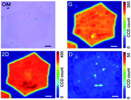
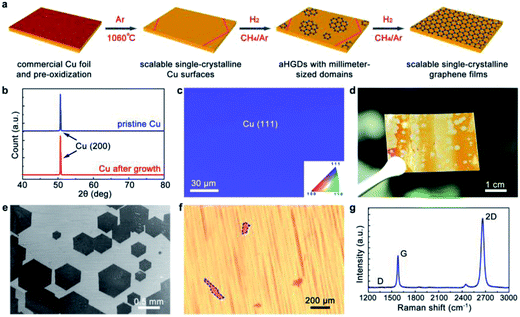
The growth procedure of the aHGDs is illustrated in Fig. 1a. A commercially available Cu foil (#46365 from Alfa Aesar China Chemical Co., Ltd.) is simply heated at 200–350 °C for 10–30 min in the air to form an oxide layer before it is placed into a CVD chamber. The sequent short-time hydrogen (H2)-free annealing process reconstructs the Cu foil surface for a centimeter scale monocrystallization to the (111) texture. Although the X-ray diffraction (XRD, Fig. 1b) spectra show that both the pristine and annealed Cu foils are dominated by the (100) texture, further investigation on the annealed Cu foil by electron backscatter diffraction (EBSD, Fig. 1c) clearly reveals the presence of a homogenous surface with the (111) texture over a large area. Considering that EBSD reflects more structural information within the several-nanometer depth near the crystal surface, it is clear that a uniform thin Cu (111) layer is formed on top of the pristine polycrystalline Cu foil. Fig. 1d displays an image of the as-grown graphene domains on the reconstructed Cu foil with the control parameter (pre-oxidation at 300 °C for 30 min and 60 min growth). The color contrast of graphene is realized by slightly oxidizing the as-grown Cu foil in the air.20 The sizes of these graphene domains are approximately 0.5–2.5 millimeters, indicating a maximum growth rate of higher than 40 μm min−1. The scanning electron microscopy (SEM) image of the graphene domains with a shorter growth period of 0.5 hour is shown in Fig. 1e. All the graphene domains observed in the image are unidirectionally aligned on the Cu surface with a misorientation angle of less than 1° as well as a hexagonal shape with straight edges. Similar results of these aligned hexagonal graphene domains (aHGDs) were reproduced on other types of commercial Cu foils (Fig. S1, ESI†), indicating that the oxide-assisted surface monocrystallization was irrelevant to the Cu production process. It also needs to be noted that the growth results of these aHGDs are not influenced by a prolonged annealing process with H2; this indicates that a changed reduction gas atmosphere does not affect the established surface monocrystallinity of Cu (Fig. S2, ESI†). Moreover, the growth rate of a graphene film formed by aHGDs can be tuned by modifying the Cu pre-oxidation parameters (i.e., temperature and time) for different nucleation densities of the domain, as shown in Fig. S3 in ESI.† Fig. 1f shows an optical microscopy (OM) image of a graphene sample, whose domains are on the verge of totally coalescing together into a global continuous film, on Cu with the maximum film growth rate (pre-oxidation at 205 °C for 10 min and 40 min growth). The uncovered Cu regions (i.e., dark orange areas) are surrounded by the straight graphene domain edges that are parallel to each other or with an included angle of 60° or 120°; this confirms the unidirectional alignment of the coalesced graphene domains to which these edges belong. The formed continuous graphene film exhibits a sheet resistance of ∼270 ± 30 Ω □−1, close to the value reported by Xu et al. for their meter-scale graphene single crystals.19 We have performed Raman spectroscopy with a 532 nm excitation laser on the aHGDs transferred onto the SiO2/Si wafers. All of their typical Raman spectra exhibit the fingerprint of monolayer graphene with a high intensity ratio of the 2D (∼2690 cm−1) to G (∼1580 cm−1) bands, a narrow and symmetric 2D band, and a negligible D-band (∼1340 cm−1, originated from the structural defects of graphene),21 as shown in Fig. 1g, indicating the very high quality of these aHGDs.The uniformity and quality of the aHGDs were further determined by the scanning Raman maps of the intensities for the G, 2D, and D bands (Fig. 2). The graphene domain appears in a uniform contrast when inspected by OM except for the small sites due to the polymer residues from the transfer process; this indicates that the layer number is uniform across the sample. Correspondingly, in the Raman maps, most scanned areas of the graphene domain exhibit uniform G and 2D band intensity distributions except for the domain edges, and the average 2D-to-G intensity ratio is ∼1.8 ± 0.3, indicative of the monolayer nature for the whole domain. Moreover, the Raman spectra in the whole domain present relatively low D band intensities including the domain edges, which not only demonstrate the overall high quality of the graphene but also, to some extent, help confirm the zigzag edge structure for these domains; this has been further discussed hereinafter.
 | ||
| Fig. 2 The OM image and scanning Raman spectroscopy results for the G, 2D, and D bands for an aHGD transferred onto the SiO2/Si substrate. Scale bars: 100 μm. | ||
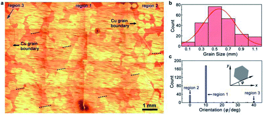
Fig. 3 further presents the alignment of these graphene domains on the Cu foil in more details by scanning the domains within a large view field (10.5 × 7.5 mm2) with a 5× microscope objective and organizing the 16 OM images together. A different growth condition with a shorter pre-oxidation and growth time is adopted in the sample to increase the nucleation density of the isolated graphene domains for the analysis. Only two grain boundaries from Cu are visible near the corners of the view field. The center region (region 1) between two Cu grain boundaries clearly demonstrates the high efficiency of Cu surface monocrystallization up to centimeter scale. The information about the size and orientation of more than 200 aHGDs grown on this Cu surface within these three regions is obtained and shown in Fig. 3b and c, respectively. The diagonal sizes of these domains range from 0.1 to 1.1 mm and are fitted well by Gaussian distribution with a center value of ∼0.57 mm. Considering that all the aHGDs have a hexagonal shape, it is characterized by the orientation angle θ relative to the horizontal line in the OM images. For all the aHGDs shown in Fig. 2b, their dominant orientation angles are 10°, 1°, and 40° and solely observed in the region 1, region 2, and region 3 (Fig. S4, ESI†), respectively. Especially, among all the 177 graphene domains measured in the region 1, only 3 of them exhibit different orientation angles other than 10°, corresponding to a unidirectional domain alignment of >98%. The abovementioned result also confirms a strict alignment of the aHGDs over a distance exceeding 1 cm scale, and similar results can also be obtained from the graphene domains in the region 2 and 3.
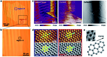
The unidirectional alignment of these aHGDs suggests a possibility of seamless stitching when they coalesce, i.e., to form a scalable single-crystalline graphene film. Therefore, it is of great significance to characterize the coalescence interfaces for the aHGDs. For this purpose, atomic force microscopy (AFM) analysis on the aligned and misaligned graphene domains and their coalescence interfaces was conducted. As shown in Fig. 4, a coalescence corner (region A in Fig. 4b) by two aHGDs is chosen for the lateral force (friction), current, and deflection (error signal) measurements, and the results are presented in Fig. 4c. Except for the regular terraces of the underlying Cu substrate, all signals are rather homogeneous within the domains as well as at the coalescence interface where a domain boundary is supposed to appear if any. By contrast, for a coalescence interface formed by two misaligned graphene domains, the clearly enhanced signals of lateral force, current, and deflection are detected, as shown in Fig. S5 in ESI.† Apparently, the contrasts of lateral force, current, and deflection signals at the coalescence interface of two graphene domains are associated with the presence of domain boundaries or overlapped step edges, resulted from the differences in the structural and physical properties at these domain coalescence interfaces. The AFM measurement results for the coalesced domains with seamless stitching can be routinely reproduced for the aligned interfaces (Fig. S6, ESI†). We have also performed the atomic-resolved AFM measurements to reveal the crystalline orientation of two aHGDs. As seen in Fig. 4d, a hexagonal lattice with a lattice constant of ∼0.25 nm can be extracted from the data, showing a perfect agreement with the known lattice constant of monolayer graphene (0.246 nm),23 and it is easy to derive that two aHGDs have the same lattice orientation. Moreover, as shown in Fig. 4e, we have indicated the zigzag directions by arrows, and apparently, the edges of both aHGDs are along this direction; this is believed to result from the metal-assisted H2 anisotropic etching process. This zigzag edge structure is also consistent with the low D-band intensities measured from the aHGD edges shown in Fig. 2.
Finally, we have further discussed the role of the Cu surface oxide layer in the growth of millimeter-sized aHGDs. We have conducted several control experiments using the conditions of (a) with and without the surface oxide and (b) heating and annealing with and without H2. As shown in Table S1 and Fig. S7 in ESI,† with surface oxide, the graphene domains with significantly increased sizes can be obtained after growth. This can be attributed to the fact that the O residues can be embedded into the Cu surface to make it featureless after the reduction.22 However, the domain alignment is only possible when H2 is introduced during the annealing process at high temperatures. This suggests that if it is not removed during the heating process, the pre-treated surface oxide layer can help to reconstruct23 and monocrystallize the Cu surface under the reduction gas atmosphere at high temperatures; this is probably due to the enhanced pre-melting effect24,25 near the Cu surface resulting from the adsorbed oxygen species to reconstruct the Cu surface for the more stable (111) textures. Moreover, the CVD growth of aHGDs with different periods, as shown in Fig. S8 in ESI,† shows that during the first several minutes of growth, only few domains nucleate on the Cu surface. This may also suggest a period for the Cu surface reconstruction by the sudden introduction of H2, which is not suitable for graphene nucleation and growth. The domains later exhibit a fast rate of ∼30 μm min−1, much faster than that without the surface oxide layer; this demonstrates that the Cu surface oxide layer can provide surface oxygen to accelerate the growth of graphene domains.11 It needs to be mentioned that although previous literature has shown that large-scale single-crystal surfaces and graphene domains can be obtained by annealing under an Ar atmosphere,18,22,26 the results in Fig. S7† clearly demonstrate the importance of both pre-treated Cu surface oxide layer and annealing under a non-reduction gas atmosphere in the enlargement and alignment of the graphene domains through the Cu surface monocrystallization.
Conclusion
In summary, we have demonstrated the CVD growth of scalable single-crystalline graphene by seamlessly stitching millimeter-sized unidirectional aHGDs on different types of commercially available Cu foils without any repeated substrate polishing and/or hydrogen annealing processes. The key factor for the growth is the surface reconstruction and monocrystallization of the Cu foils achieved by pre-introducing an oxide layer and the sequential Ar annealing. The aHGD growth shows an average growth rate of >20 μm min−1 and a misorientation possibility of <2%. The AFM lateral force, current, and deflection measurements present no differences at the domain coalescence interfaces; this clearly demonstrates the elimination of domain boundaries and seamless stitching of the domains. Compared with that reported in previous studies, the average size for our hexagonal graphene domains is enlarged by 1–2 orders of magnitude (from tens of micrometers to millimeter); this further eliminates the formation of domain boundaries. We believe that this cost-effective and time-saving synthetic method for large-scale single-crystalline graphene will be of significant attraction presenting valuable guidance for future industrial devices and applications of high-quality graphene.Experimental
Graphene synthesis
A piece of commercially available Cu foils (#46365, #13382, and #42972 from Alfa Aesar China Chemical Co., Ltd., #113243 from Nilaco Co., Ltd., etc.) was heated at 200–300 °C in the air by a hot plate for 1–30 min to create a layer of metal oxide before it was loaded into a CVD quartz chamber. For the growth of millimeter-sized aligned hexagonal graphene domains (aHGDs), an atmospheric pressure CVD process was used. The chamber temperature was increased to 1060 °C and maintained (total time: 70 min) under an atmosphere of Ar (1000 sccm) to anneal and monocrystallize the Cu surface, and the pressure inside the chamber was kept at 1 atm. For graphene growth, 20 sccm diluted CH4 (0.05% in Ar), 10 sccm H2, and 300 sccm Ar were employed. After being cooled down to room temperature, the as-grown graphene on the Cu foil was heated in the air at 160 °C for 10 min for direct visualization.20Characterizations
The characterizations of graphene were carried out by SEM (3 kV, S-3400, Hitachi Co., Ltd.), XRD (X'Pert PRO, PANalytical Co., Ltd.), micro-Raman spectroscopy (532 nm wavelength excitation laser, LabRAM HR Evolution, Horiba Co., Ltd.), OM (yellow light by Shanghai 8XB-PC from Shanghai Optical Instrument Factory and blue light by Olympus BXFM-ILHS from Olympus Co., Ltd), EBSD using scanning auger electron spectroscopy (AES, PHI-710, ULVAC-PHI Inc.), AFM (Multimode 8 system equipped with a silicon probe SNL-10 from Bruker Co., Ltd.), and high-resolution AFM/STM (NT-MDT spectrum Instruments).Conflicts of interest
There are no conflicts to declare.Acknowledgements
A part of this work was financially supported by the National Key Scientific Instruments and Equipment Development Project of China (61427901), the National Science Foundation of China (11502231, 11621062, 61471317), and the Fundamental Research Funds for the Central Universities (2017QNA4032).References
- X. S. Li, W. W. Cai, J. H. An, S. Kim, J. Nah, D. X. Yang, R. Piner, A. Velamakanni, I. Jung, E. Tutuc, S. K. Banerjee, L. Colombo and R. S. Ruoff, Science, 2009, 324, 1312–1314 CrossRef CAS PubMed.
- S. Bae, H. Kim, Y. Lee, X. Xu, J.-S. Park, Y. Zheng, J. Balakrishnan, T. Lei, H. Ri Kim, Y. I. Song, Y.-J. Kim, K. S. Kim, B. Ozyilmaz, J.-H. Ahn, B. H. Hong and S. Iijima, Nat. Nanotechnol., 2010, 5, 574–578 CrossRef CAS PubMed.
- X. Li, L. Colombo and R. S. Ruoff, Adv. Mater., 2016, 28, 6247–6252 CrossRef CAS PubMed.
- P. Y. Huang, C. S. Ruiz-Vargas, A. M. van der Zande, W. S. Whitney, M. P. Levendorf, J. W. Kevek, S. Garg, J. S. Alden, C. J. Hustedt, Y. Zhu, J. Park, P. L. McEuen and D. A. Muller, Nature, 2011, 469, 389–392 CrossRef CAS PubMed.
- L. Tapasztó, P. Nemes-Incze, G. Dobrik, K. Jae Yoo, C. Hwang and L. P. Biró, Appl. Phys. Lett., 2012, 100, 053114 CrossRef.
- Z. Song, V. I. Artyukhov, B. I. Yakobson and Z. Xu, Nano Lett., 2013, 13, 1829–1833 CrossRef CAS PubMed.
- Z. Fei, A. S. Rodin, W. Gannett, S. Dai, W. Regan, M. Wagner, M. K. Liu, A. S. McLeod, G. Dominguez, M. Thiemens, H. Castro Neto Antonio, F. Keilmann, A. Zettl, R. Hillenbrand, M. M. Fogler and D. N. Basov, Nat. Nanotechnol., 2013, 8, 821–825 CrossRef CAS PubMed.
- X. Li, C. W. Magnuson, A. Venugopal, R. M. Tromp, J. B. Hannon, E. M. Vogel, L. Colombo and R. S. Ruoff, J. Am. Chem. Soc., 2011, 133, 2816–2819 CrossRef CAS PubMed.
- Z. Yan, J. Lin, Z. Peng, Z. Sun, Y. Zhu, L. Li, C. Xiang, E. L. Samuel, C. Kittrell and J. M. Tour, ACS Nano, 2012, 6, 9110–9117 CrossRef CAS PubMed.
- H. Zhou, W. J. Yu, L. Liu, R. Cheng, Y. Chen, X. Huang, Y. Liu, Y. Wang, Y. Huang and X. Duan, Nat. Commun., 2013, 4, 2096 Search PubMed.
- Y. Hao, M. S. Bharathi, L. Wang, Y. Liu, H. Chen, S. Nie, X. Wang, H. Chou, C. Tan, B. Fallahazad, H. Ramanarayan, C. W. Magnuson, E. Tutuc, B. I. Yakobson, K. F. McCarty, Y.-W. Zhang, P. Kim, J. Hone, L. Colombo and R. S. Ruoff, Science, 2013, 342, 720–723 CrossRef CAS PubMed.
- X. Chen, P. Zhao, R. Xiang, S. Kim, J. Cha, S. Chiashi and S. Maruyama, Carbon, 2015, 94, 810–815 CrossRef CAS.
- V. L. Nguyen, B. G. Shin, D. L. Duong, S. T. Kim, D. Perello, Y. J. Lim, Q. H. Yuan, F. Ding, H. Y. Jeong, H. S. Shin, S. M. Lee, S. H. Chae, Q. A. Vu, S. H. Lee and Y. H. Lee, Adv. Mater., 2015, 27, 1376–1382 CrossRef CAS PubMed.
- V. L. Nguyen and Y. H. Lee, Small, 2015, 11, 3512–3528 CrossRef CAS PubMed.
- H. Wang, X. Xu, J. Li, L. Lin, L. Sun, X. Sun, S. Zhao, C. Tan, C. Chen, W. Dang, H. Ren, J. Zhang, B. Deng, A. L. Koh, L. Liao, N. Kang, Y. Chen, H. Xu, F. Ding, K. Liu, H. Peng and Z. Liu, Adv. Mater., 2016, 28, 8968–8974 CrossRef CAS PubMed.
- L. Sun, L. Lin, J. Zhang, H. Wang, H. Peng and Z. Liu, Nano Res., 2017, 10, 355–363 CrossRef CAS.
- M. Zeng, L. Tan, L. Wang, R. G. Mendes, Z. Qin, Y. Huang, T. Zhang, L. Fang, Y. Zhang, S. Yue, M. H. Rümmeli, L. Peng, Z. Liu, S. Chen and L. Fu, ACS Nano, 2016, 10, 7189–7196 CrossRef CAS PubMed.
- J. Hu, J. Xu, Y. Zhao, L. Shi, Q. Li, F. Liu, Z. Ullah, W. Li, Y. Guo and L. Liu, Sci. Rep., 2017, 7, 45358 CrossRef CAS PubMed.
- X. Xu, Z. Zhang, J. Dong, D. Yi, J. Niu, M. Wu, L. Lin, R. Yin, M. Li, J. Zhou, S. Wang, J. Sun, X. Duan, P. Gao, Y. Jiang, X. Wu, H. Peng, R. S. Ruoff, Z. Liu, D. Yu, E. Wang, F. Ding and K. Liu, Sci. Bull., 2017, 62, 1074–1080 CrossRef.
- C. Jia, J. Jiang, L. Gan and X. Guo, Sci. Rep., 2012, 2, 707 CrossRef PubMed.
- A. C. Ferrari, J. C. Meyer, V. Scardaci, C. Casiraghi, M. Lazzeri, F. Mauri, S. Piscanec, D. Jiang, K. S. Novoselov, S. Roth and A. K. Geim, Phys. Rev. Lett., 2006, 97, 187401 CrossRef CAS PubMed.
- J. Li, X. Wang, X. Liu, Z. Jin, D. Wang and L. Wan, J. Mater. Chem. C, 2015, 3, 3530 RSC.
- A. Y. Lu, S. Y. Wei, C. Y. Wu, Y. Hernandez, T. Y. Chen, T. H. Liu and Z. Y. Juang, RSC Adv., 2012, 2, 3008 RSC.
- J. W. M. Frenken and J. F. v. d. Veen, Phys. Rev. Lett., 1985, 54, 134–137 CrossRef CAS PubMed.
- Z.-J. Wang, G. Weinberg, Q. Zhang, T. Lunkenbein, A. Klein-Hoffmann, M. Kurnatowska, M. Plodinec, Q. Li, L. Chi, R. Schloegl and M.-G. Willinger, ACS Nano, 2015, 9, 1506–1519 CrossRef CAS PubMed.
- L. Gan and Z. Luo, ACS Nano, 2013, 7, 9480–9488 CrossRef CAS PubMed.
Footnote |
| † Electronic supplementary information (ESI) available: Supplementary Figures. See DOI: 10.1039/c8ra00770e |
| This journal is © The Royal Society of Chemistry 2018 |


