
 Open Access Article
 This Open Access Article is licensed under a Creative Commons Attribution-Non Commercial 3.0 Unported Licence
The investigation of in situ removal of Si substrates for freestanding GaN crystals by HVPE†
Moonsang Lee‡
 *a,
Dmitry Mikulik‡b and
Sungsoo Park*cd
*a,
Dmitry Mikulik‡b and
Sungsoo Park*cd
aKorea Basic Science Institute, 169-148, Gwahak-ro, Yuseong-gu, Daejeon, Korea, Republic of Korea. E-mail: lms1015@kbsi.re.kr
bLaboratory of Semiconductor Materials, Ecole Polytechnique Fédérale de Lausanne 1015, Lausanne, Switzerland
cDepartment of Science Education, Jeonju University, 303 Cheonjam-ro, Wansan-gu, Jeollabuk-do, Republic of Korea. E-mail: sspark@jj.ac.kr
dAnalytical Lab of Advanced Ferroelectric Crystals, Jeonju University, 303 Cheonjam-ro, Wansan-gu, Jeollabuk-do, Republic of Korea
First published on 29th March 2018
Abstract
We investigate the etching of a Si substrate in the fabrication process of freestanding GaN crystal grown using a Si by HVPE. Followed by crystal growth, Si etching by vapor HCl at high temperature results in successful fabrication of the freestanding GaN. Due to the complicated vertical gas flows inside the reactor, careful design of the susceptor was implemented. The unintentional formation of SixNy thin layer at the backside of the Si substrate after the epitaxial growth, which can cause the decreased etch rate and non-uniform etching of a Si substrate, was successfully prevented by N2 purging during and after the etching of a Si substrate. We believe that this study will guide us to achieve the growth of freestanding GaN over 8-inch diameters in the efficient and practical way.
Introduction
The fabrication of reliable nitride devices such as optoelectric (blue and ultraviolet light emitting diodes) and power electronics requires high quality GaN crystals as a substrate.1–5 Since the lack of native GaN, a number of methods such as hydride vapor phase epitaxy (HVPE),6 high temperature high pressure (HTHP),7 ammonothermal8 and Na flux9 have been investigated to produce GaN materials. Among these things, HVPE is the most promising epitaxial method for bulk GaN growth due to its high growth rate (100–300 μm h−1), low production cost, and relatively high quality (TDD < 1 × 107 cm−2).10,11 For the growth of HVPE GaN, foreign substrates such as sapphire (Al2O3), and GaAs have been used. Depending on the substrate materials, several separation techniques have been reported to obtain freestanding GaN so far. M. K. Kelly et al. used a laser-induced lift-off technique to separate thick GaN crystals from the sapphire substrates.12,13 Motoki et al. obtained freestanding GaN wafers by removing GaAs substrates with aqua regia.14,15 Freestanding GaN wafers were also obtained by separating thick GaN layers from NdGaO3 or LiAlO2 substrates by thermal stress.16,17 Furthermore, K. Kachel et. al. reported that freestanding GaN could be achieved on β-Ga2O3 (100) using an intermediate low temperature buffer layer by in situ NH3 treatment of substrate.18 All these separation processes require additional step outside of HVPE system thus complicating the fabrication of GaN substrates. Furthermore, several barriers such as wafer size limit and cost restrict the commercial use of HVPE GaN substrates.Recently, we reported on the high quality freestanding GaN with an etch pit density (EPD) of about 1 × 106 cm−2 over the 2-inch wafer grown using a Si substrate by chemical etching of substrate material after GaN growth.19,20 Even if the EPD of the freestanding GaN crystal obtained using in situ removal of a Si substrate fall short of EPD for homoepitaxially-grown material (∼104 cm−2), its value is comparable to commercial HVPE freestanding GaN grown on Al2O3 substrates (TDD < 1 × 107 cm−2).21 This technique will allow us to obtain freestanding GaN wafer with a large scale and low fabrication cost, thus enabling to lead to their successful commercialization. Considering the importance of the growth of freestanding GaN via in situ removal of a Si substrate, the understanding of the Si etching in HVPE should be addressed for successful implementation. In other words, the growth of freestanding GaN using in situ removal of a Si substrate cannot be achieved without complete and uniform etching of substrate material, which can give rise to crack and non-uniform thickness in GaN layers. In this paper, we give insights on the Si etching in the proposed method to grow freestanding GaN from a Si substrate by HVPE.
Experimental
To realize the growth of freestanding GaN from a Si substrate, home-made vertical type HVPE reactor with 4′′ diameter was used as shown in Fig. 1. A 2 inch (111) Si wafer with AlN/Al0.4Ga0.6N/GaN buffer layers grown by metalorganic chemical vapor deposition (MOCVD) was used as a substrate for the deposition of a thick GaN layer. The growth process is reported elsewhere in details.19,20 Briefly, GaN was grown at 1080 °C in atmosphere pressure with V/III ratio of 20. The Si etching was performed using 200 sccm HCl gas flow at 1000 °C after the growth of a thick GaN layer. The temperature was controlled by a thermocouple passing through resistive heater, which was 5 cm away from the substrate. HCl gas diluted with N2 was supplied from the bottom of the reactor through the additional channel. The inset of Fig. 1 illustrates the schematics of the part of wafer-loading zone in the HVPE reactor where the in situ removal of Si substrate was achieved by implementing special quartz parts and susceptor design. HCl gas can flow through the quartz susceptor from bottom side of the support in HVPE reactor as shown by yellow arrows in Fig. 1b. In addition, we employed N2 purging before and during the etching process to control the Si etching rate and prevent incorporation of GaN growth by-products on the backside of Si wafer. Without N2 purging after the epitaxial growth, parasitic SixNy film was formed on the back side of the Si substrate, by which prevented Si etching by HCl. Transmission electron microscopy (TEM) and energy dispersive X-ray spectroscopy (EDX) analysis were used to study the backside of Si wafer.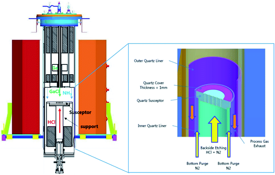 | ||
| Fig. 1 Schematic diagram of the home-made vertical HVPE reactor and growth/etch zone of the HVPE reactor. | ||
Results and discussion
In the chemical etching process, the Si substrate is exposed to HCl gas flow directed through the quartz susceptor, which has one or multiple holes. The substrate undergoes thermal dry etching and silicon tetrachloride and hydrogen gas form according to the following reaction:22| Si + xHCl (g) → SiH4−xClx (g) + (x − 2)H2 (g) | (1) |
Previously, we discussed the optimal temperature to etch Si substrate in order to avoid the undesirable tensile stress between the substrate and GaN.19,20 We found that the maximum in-plane stress can be minimized to −0.07 MPa at 1000 °C being slightly compressive and allowing the implementation of Si etching. However, the uniformity of Si etching rate over 2-inch wafer surface is another important factor to obtain crack-free freestanding GaN. The presence of un-etched completely Si substrate during cooling down can generate micro-cracks and lead to the cracks of the freestanding GaN. To perform complete and uniform etching of Si substrates, rotating susceptors with different shape design were fabricated and tested on Si dummy wafers. Susceptor types 1 and 2 represent multi-openings design and susceptor types 3 and 4 – single large opening design, as shown in Fig. 2a. Fig. 2b shows the etch rate of Si substrates as a function of wafer positions in different shape of the susceptor with fixed HCl flow at 200 sccm. It is noticeable that single opening design of susceptors with a larger open area of Si substrates to HCl gas flow has better uniformity than the multi-openings susceptor design. Moreover, the highest non-uniformity within the wafer was found at the edges of the wafer. Based on these results, susceptor 4 was used in the experiment with etching Si wafer after GaN deposition in HVPE.
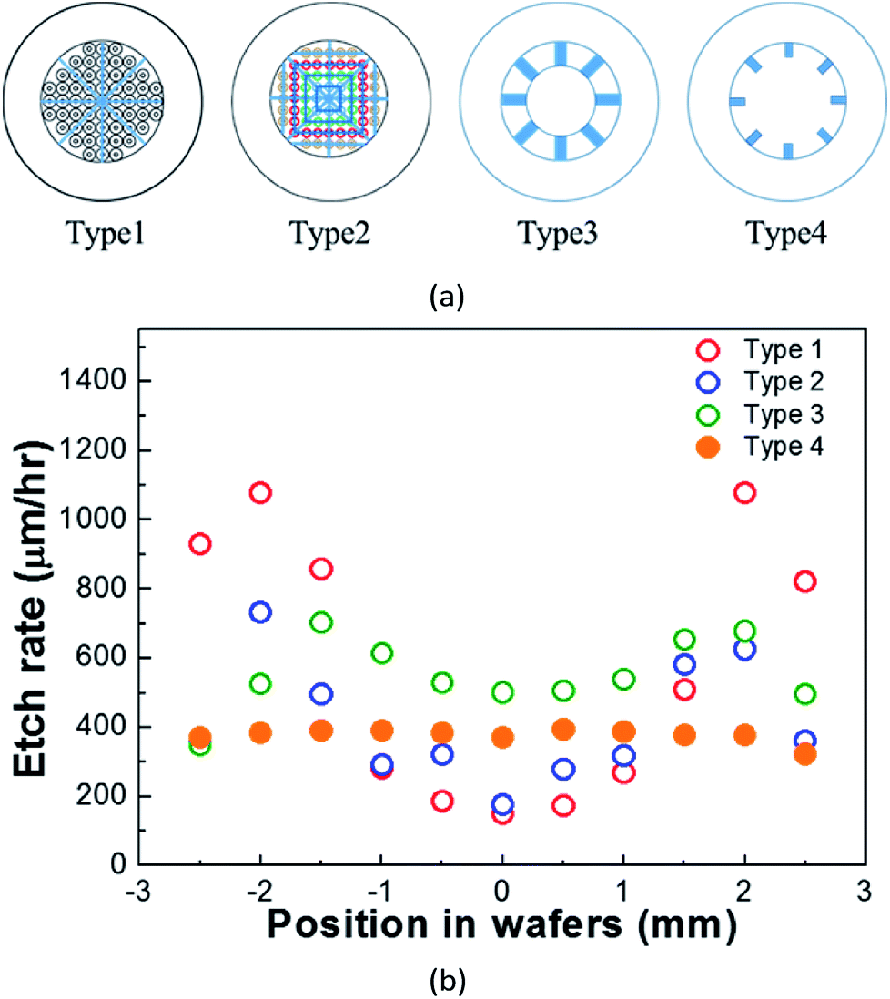 | ||
| Fig. 2 (a) Susceptor types used during the etching of Si substrate (b) etch rate uniformity over the Si wafer for different susceptors at fixed HCl flow 200 sccm. | ||
Indeed, the position of Si substrate in susceptor needs to be considered as well during optimization of the etch rate uniformity. Biased position of Si substrate on susceptor can make HCl gas flow deviation, resulting in etching rate difference. Fig. 3a shows the schematic drawing of Si wafer loaded with the offset to the central position. Note that wide spacing between Si substrate and susceptor leads the high etch rate of Si substrate near the edge as shown in Fig. 3b. As a result, GaN can be etched/decomposed by high temperature under HCl ambient. The reaction of HVPE GaN film with the HCl gas can be expressed as the following decomposition route:23
| 4GaN + 2HCl (g) → 2Ga (l) + 2GaCl (g) + H2 (g) + 2N2 (g) | (2) |
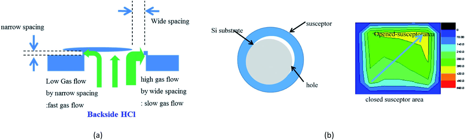 | ||
| Fig. 3 (a) Out of center-loading of a Si substrate on susceptor vs. HCl flow rate, and (b) etch rate of a Si substrate. | ||
To clarify the Si removal by the HVPE reactor, we preliminarily tested the etching of Si substrates without growing HVPE GaN. The Si substrates were successfully and uniformly removed with the etch rate of 390 μm h−1 by backside HCl gas with the flow rate of 200 sccm at 1000 °C. However, after growing the HVPE GaN, the Si substrates were not completely etched away when applying even the etch time of 180 min at the same ambient. This ascribed the unintentional and non-uniform SixNy deposition on the backside of Si substrates.
During HVPE GaN growth, GaCl and NH3 gas were incorporated into the growth zone in HVPE reactor. The residual NH3 and HCl species, not reacted during GaN growth, can exist below the growth zone. Therefore, SixNy can be formed on the backside of Si substrates during or before the Si etch step as follows:
| xSiCl4 (g) + 2H2 (g) + yNH3 (g) → SixNy + 4HCl (g) + 3/2yH2 (g) | (3) |
To investigate the formation of SixNy on the back side of the Si wafer, we analyzed the sample with EDX and TEM. Fig. 4a illustrates the cross-sectional TEM image on the backside of Si substrate after growing HVPE GaN and followed by the removal of Si substrate in HVPE reactor. This clearly shows that undesirable layer was deposited on the backside of a Si substrate during in situ etch process. As shown in Fig. 4b, EDX confirmed the formation of SixNy on the backside of a Si substrate. From the TEM image, we can conclude amorphous phase of SixNy with approximately 3 nm in thickness.
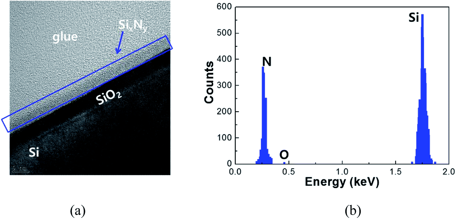 | ||
| Fig. 4 (a) Cross-sectional TEM image of the backside on a Si substrate after etching Si substrate in HVPE reactor; (b) EDS data on the backside of a Si substrate after growing GaN and then applying in situ etch of Si substrate in HVPE reactor. | ||
To prevent the deposition of SixNy on the backside of Si substrates, the purge step in N2 ambient was added before in situ removal of Si substrates and during HVPE GaN growth in the backside channel, by which the formation of SixNy was successfully neglected.
Indeed, the flow rate of backside gas, the configuration of susceptors, and the position of Si substrate in susceptors influence on the rate and uniformity of the Si etching. Finally, Si substrates with unintentional SixNy deposition were etched in 150 min completely.
Finally, a 400 μm-thick freestanding GaN with 2 inches in diameter was achieved via HVPE growth and in situ removal of a Si substrate as shown in Fig. 5a. The surface morphology of as-grown freestanding GaN grown using a Si substrate exhibited the root mean square (RMS) of about 0.37 nm. (See Fig. S2†) The shape of freestanding GaN crystals grown from Si substrates was slight concave with the bowing of about 5 μm/2 inch, implying the presence of tensile stress in GaN layers.24 This is attributed to the difference of defect densities between Ga- and N-faces of the freestanding GaN.25 It was estimated to be the FWHM difference of ∼130 arcsec in (002) X-ray rocking curves. Additionally, the wafer bowing of 5 μm/2 inch corresponds to the curvature radius of ∼60 m. Finally, we can observe that the freestanding GaN was successfully grown from Si substrates without any meltback, pits or cracks as illustrated in Fig. 5b. The values of FWHM for (002) and (102) reflection in X-ray rocking curves were estimated to be 67 arcsec and 96 arcsec, respectively, as shown in Fig. 5c. Furthermore, threading dislocation density of freestanding GaN crystals obtained from in situ removal of a Si substrate was confirmed by micro-PL mapping, as seen in Fig. 5d. This revealed that the threading dislocation densities were evaluated about 1 × 106 cm−2.
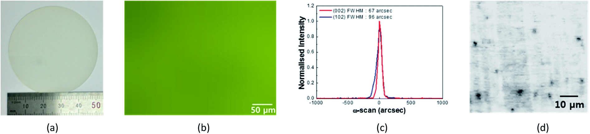 | ||
| Fig. 5 (a) A photograph image of a freestanding GaN crystal grown using a Si substrate. (b) Plan-view optical microscopy image of a freestanding GaN crystal grown using a Si substrate. (c) (002) and (102) X-ray rocking curve of freestanding GaN grown via in situ removal of a Si substrate. (d) Micro PL map of a 50 × 50 μm2 area of a freestanding GaN crystal with 400 μm in thickness grown using in situ removal of a Si substrate. The dark spots represent low PL emission intensity, indicating the dislocation sites. | ||
Conclusions
During the fabrication of freestanding GaN from Si substrate by HVPE, uniform and complete etching of Si was realized. From prelaminar experiments on Si test wafers, we found the optimal susceptor design with the single large opening.Loading effect was found detrimental to the fabrication process due to GaN etching/decomposition risk under HCl ambient at high temperature. Finally, N2 purge step helps to avoid unintentional SixNy formation on the backside of the Si wafer, thus preventing Si etching by HCl. We believe that HVPE growth followed by a Si substrate etching will open a new path to obtain freestanding GaN wafer over 8 inches with relatively low defect density.
Conflicts of interest
There are no conflicts to declare.Acknowledgements
This research was supported by Basic Science Research Program through the National Research Foundation of Korea (NRF) funded by the Ministry of Education (2016R1A6A1A03012069).References
- C.-L. Chao, R. Xuan, H.-H. Yen, C.-H. Chiu, Y.-H. Fang, Z.-Y. Li, B.-C. Chen, C.-C. Lin, C.-H. Chiu and Y.-D. Guo, IEEE Photonics Technol. Lett., 2011, 23, 798–800 CrossRef CAS.
- Y. Kuwahara, T. Fujii, Y. Fujiyama, T. Sugiyama, M. Iwaya, T. Takeuchi, S. Kamiyama, I. Akasaki and H. Amano, Appl. Phys. Express, 2010, 3, 111001 CrossRef.
- M. Maier, K. Köhler, M. Kunzer, J. Wiegert, S. Liu, U. Kaufmann and J. Wagner, Phys. Status Solidi C, 2008, 5, 2133–2135 CrossRef CAS.
- D. J. Meyer, D. A. Deen, D. F. Storm, M. G. Ancona, D. S. Katzer, R. Bass, J. A. Roussos, B. P. Downey, S. C. Binari and T. Gougousi, IEEE Electron Device Lett., 2013, 34, 199–201 CrossRef CAS.
- Z. Vashaei, E. Cicek, C. Bayram, R. McClintock and M. Razeghi, Appl. Phys. Lett., 2010, 96, 201908 CrossRef.
- J. Freitas Jr, J. Culbertson, N. Mahadik, T. Sochacki, M. Bockowski and M. Iwinska, Cryst. Growth Des., 2015, 15, 4837–4842 Search PubMed.
- B. Sadovyi, A. Nikolenko, J. Weyher, I. Grzegory, I. Dziecielewski, M. Sarzynski, V. Strelchuk, B. Tsykaniuk, O. Belyaev and I. Petrusha, J. Cryst. Growth, 2016, 449, 35–42 CrossRef CAS.
- Q. Bao, T. Hashimoto, F. Sato, K. Hazu, M. Saito, Y. Kagamitani, T. Ishinabe, R. Kayano, D. Tomida and K. Qiao, CrystEngComm, 2013, 15, 5382–5386 RSC.
- S. Takeuchi, H. Asazu, M. Imanishi, Y. Nakamura, M. Imade, Y. Mori and A. Sakai, J. Appl. Phys., 2015, 118, 245306 CrossRef.
- E. Richter, M. Gründer, B. Schineller, F. Brunner, U. Zeimer, C. Netzel, M. Weyers and G. Tränkle, Phys. Status Solidi C, 2011, 8, 1450–1454 CrossRef CAS.
- M. Weyers, E. Richter, C. Hennig, S. Hagedorn, T. Wernicke and G. Tränkle, Light-emitting diodes: research, manufacturing, and applications XII, Proc. SPIE, 2008, 6910, 69100l CrossRef.
- M. K. Kelly, R. P. Vaudo, V. M. Phanse, L. Görgens, O. Ambacher and M. Stutzmann, Jpn. J. Appl. Phys., 1999, 38, L217 CrossRef CAS.
- C. R. Miskys, M. K. Kelly, O. Ambacher and M. Stutzmann, Phys. Status Solidi C, 2003, 1627–1650 CrossRef CAS.
- K. Motoki, T. Okahisa, N. Matsumoto, M. Matsushima, H. Kimura, H. Kasai, K. Takemoto, K. Uematsu, T. Hirano and M. Nakayama, Jpn. J. Appl. Phys., 2001, 40, L140 CAS.
- T. Nakamura and K. Motoki, Proc. IEEE, 2013, 101, 2221–2228 CrossRef CAS.
- E. Richter, C. Hennig, L. Wang, U. Zeimer, M. Weyers and G. Tränkle, Phys. Status Solidi C, 2007, 4, 2277–2280 CAS.
- A. Wakahara, Hydride Vapor Phase Epitaxy of GaN on NdGaO3 Substrate and Realization of Freestanding GaN Wafers with 2-inch Scale, Jpn. J. Appl. Phys., 2000, 39, 2399 CrossRef CAS.
- K. Kachel, M. Korytov, D. Gogova, Z. Galazka, M. Albrecht, R. Zwierz, D. Siche, S. Golka, A. Kwasniewski and M. Schmidbauer, CrystEngComm, 2012, 14, 8536–8540 RSC.
- M. Lee, D. Mikulik, J. Kim, Y. Tak, J. Kim, M. Shim, Y. Park, U. Chung, E. Yoon and S. Park, Appl. Phys. Express, 2013, 6, 125502 CrossRef.
- M. Lee, D. Mikulik, M. Yang and S. Park, Sci. Rep., 2017, 7, 8587 CrossRef PubMed.
- T. Sochacki, M. Amilusik, M. Fijalkowski, M. Iwinska, B. Lucznik, J. L. Weyher, G. Kamler, R. Kucharski, I. Grzegory and M. Bockowski, Phys. Status Solidi B, 2015, 252, 1172–1179 CrossRef CAS.
- S. Noda, K. Tanabe, T. Yahiro, T. Osawa and H. Komiyama, J. Electrochem. Soc., 2004, 151, C399–C404 CrossRef CAS.
- M. Mastro, O. Kryliouk, M. Reed, T. Anderson, A. Davydov and A. Shapiro, Phys. Status Solidi A, 2001, 188, 467–471 CrossRef CAS.
- H. Liu, S. Dolmanan, L. Zhang, S. Chua, D. Chi, M. Heuken and S. Tripathy, J. Appl. Phys., 2013, 113, 023510 CrossRef.
- S. S. Park, I.-W. Park and S. H. Choh, Jpn. J. Appl. Phys., 2000, 39, L1141 CAS.
Footnotes |
| † Electronic supplementary information (ESI) available. See DOI: 10.1039/c8ra01347k |
| ‡ These authors equally contributed to this work. |
| This journal is © The Royal Society of Chemistry 2018 |