 Open Access Article
Numerical study of a wide-angle polarization-independent ultra-broadband efficient selective metamaterial absorber for near-ideal solar thermal energy conversion
Dong Wua,
Chang Liua,
Yumin Liu *a,
Zenghui Xua,
Zhongyuan Yua,
Li Yuab,
Lei Chena,
Rui Maa,
Jinqiannan Zhanga and
Han Yea
aState Key Laboratory of Information Photonics and Optical Communications, Beijing University of Posts and Telecommunications, Beijing 100876, China. E-mail: microliuyumin@hotmail.com
bSchool of Science, Beijing University of Posts and Telecommunications, Beijing 100876, China
First published on 8th June 2018
Abstract
Highly efficient solar absorption is very promising for many practical applications, such as power generation, desalination, wastewater treatment and steam generation. Nevertheless, so far, near-ideal solar thermal energy conversion is still difficult to achieve, which requires a near-perfect absorption from the UV to the near-infrared region and meanwhile a mid-and-far infrared absorption close to zero. Here, by employing FEM and FDTD methods respectively, a nearly omnidirectional ultra-broadband efficient selective solar absorber based on a nanoporous hyperbolic metamaterial (HMM) structure is proposed and numerically demonstrated, which can achieve an extremely high average absorption efficiency above 98.9% within the range of 260–1580 nm. More significantly, in the respect of physical mechanism, the near-perfect solar absorption of this multilayered nanostructures is primarily due to the excitation of magnetic and electric resonances resulting from localized surface plasmon resonance at metal/dielectric interfaces, working completely different from those previously reported tapered multilayered absorbers associated with the slow-light effect. Besides, for retaining heat, a low emissivity is realized in mid-infrared region, causing a near-ideal total solar-thermal conversion efficiency up to 90.32% at 373.15 K (ηideal = 95.6%), which is particularly useful in solar steam generation. Detailed studies are also performed for higher operating temperatures, which indicates efficient solar thermal conversions also can be well maintained by tuning geometric parameters at higher temperatures. Taking into consideration of the practical application, even with ±60 degrees angle of incidence, average absorptivity higher than 90% can be still obtained in the whole solar spectrum at both TE and TM polarization. The near-perfect absorption, wide angle, polarization independence, spectral selectivity and high tunability make this solar absorber promising for practical applications in solar energy harvesting.
1 Introduction
The sun is a promising, clean and abundant source of renewable energy, which can satisfy the world's energy demands and meanwhile it can effectively solve the problem of the environmental pollution coming from fossil fuels.1–10 As a commonly used and important approach to utilizing solar energy, solar thermal systems can convert solar radiation into heat, which can be directly applied in many practical applications, such as desalination, distillation and wastewater treatment and other industrial processes.1–8,11–23 Besides, for thermophotovoltaic devices, the thermal energy also can be converted to electricity.1,4,17–23 Owing to the utilization of nearly the whole solar spectrum, the thermophotovoltaic devices have recently been demonstrated to achieve higher solar-to-electrical conversion efficiency compared to photovoltaic cell alone.1 In these applications of solar thermal systems, the solar absorbers, as a key component, have a great influence on the performance of the whole system. In order to maximize the total photothermal conversion efficiency of solar absorbers, the spectrally selective absorption is very essential, which means that the solar absorber possesses an efficient solar absorption and simultaneously suppresses mid-infrared emission.6 Therefore, the study of near-ideal solar absorbers is of fundamental importance for many promising applications, and the improvement in the performance of solar absorbers would greatly promote the solar-thermal industry. Unfortunately, the design of these solar absorbers with strong spectral selectivity, near-perfect solar absorption, angular independence and polarization independence are still difficult.6Recently, plasmonic metamaterial solar absorbers have attracted a lot of attention, and many approaches have been explored for near-perfect absorption.24–65 The high absorption is mainly produced by the excitation of the localized surface plasmon resonances(LSPR) or delocalized surface plasmon resonances at the metal/dielectric interfaces. However, many metamaterial absorbers based on surface plasmon resonances (SPR) usually suffer from the disadvantage of narrow operating wave band, which greatly restricts their applications and developments in many particular applications such as solar energy harvesting. Yet recent demonstrations show that it can be harnessed using mechanisms such as multiple resonances, impedance matching, and slow-light modes to create broadband absorption.25–37 Particularly, the metamaterial nanostructures by utilizing metal/dielectric stacks are the most widely used way to realize broadband high absorption at present, which are explained by slow light characteristics in the multi-layer metal/dielectric stack.25–37 These metal/dielectric multilayer structures are proposed as one kind of hyperbolic metamaterial (HMM). For example, Cui et al. numerically presented a broadband saw-toothed infrared absorber made of alternating layers of gold and germanium layers, which realize an absorption over 95% in the wavelength ranging from 3 to 5.5 μm;25 Liang et al. numerically demonstrated a two-dimensional ultra-broadband pyramid absorber having a high absorption performance at the range of 1–14 μm, which is based on the metamaterial structure utilizing 15 gold/Ge pairs;30 Lin et al. theoretically investigated a nano-cone array formed by alternating W and Ge thin films, which can realize an average absorption approaching 98% in the wavelength range of 0.3–9 μm;34 Obviously, while realizing broadband operating ranges in these studies, the poor selectivity of absorption spectra is a serious drawback of these tapered multilayered absorbers for solar energy harvesting. According to Kirchhoff's law, these absorbers also have high thermal radiation in mid-and-far infrared region, which will significantly decrease their total solar-thermal energy conversion efficiency and hence greatly limit their further applications in solar thermal systems. Besides, these tapered structures are not benefit for large-area fabrication. Recently, the another kind of ultra-broadband solar absorbers are proposed and fabricated by self-assembly of the metal nanoparticles into a 3D nanoporous template, which will facilitate the large-scale fabricating of nanostructures and devices.5,8,35,36 For example, Zhou et al. demonstrated an efficient solar absorber fabricated by the self-assembly of aluminium nanoparticles into a three-dimensional porous membrane, which has a high absorption at the wavelengths range from 400 to 2500 nm.5 Zhou et al. also proposed a plasmonic solar absorber achieving an average absorption up to 99% over the wavelengths from 400 nm to 10 μm, which is fabricated through self-assembly of Ag nanoparticles onto a nanoporous template. Obviously, these plasmonic absorbers also have poor selectivity of absorption spectrum, possessing very high emissivity in the mid-and-far infrared region where heat loss occurs.8 To our knowledge, the reported selective solar absorption are mainly realized by these broadband absorbers based on the nanostructures constructed by arraying different nano-sized resonators in one plane to combine multiple plasmonic resonances.38–45 For example, Aydin et al. proposed and demonstrated a plasmonic absorber capable of selective high absorption over the visible spectrum(400–700 nm) owing to the symmetric arrangement of crossed trapezoid array geometry.37 However, this absorber only can realize broadband high absorptions in the visible region and cannot satisfy the spectral requirements for solar energy absorption. The improvement of absorption is still required at the ultraviolet (250–400 nm) and the near-infrared (800–2000 nm) region, which is important for estimation of the overall efficiency of the solar absorber. Wan et al. investigated a patterned gold-carbon-gold structure to realize a metasurface absorber, which has a selective high absorption from 400 to 1200 nm.38 Wang et al. proposed and experimentally demonstrated a highly efficient absorber consisting of titanium–MgF2–tungsten structure, which achieve a near-perfect absorption above 90% range from 400 nm to 2000 nm.39 The selective solar absorber achieves a high absorption in visible and NIR region, and a low emissivity in the MIR bands. However, these two selective solar absorbers, reported by Wan et al. and Wang et al., both have a relatively low absorption (<90%) in UV region and the absorption drops significantly below 90% at the middle of the high absorption band, where the absorption efficiency should be improved to achieve a near-ideal solar thermal energy conversion. The absorption of these selective solar absorbers also will deteriorate significantly with the increasing the incident angles for TE polarized incident wave, which will greatly limit their further applications in practice. Note that, most of current selective solar absorbers also suffer from these three fundamental problems: (i) the low absorption efficiency in UV region; (ii) the absorption efficiency dropping at the middle of the high absorption band; (iii) angle-dependent absorption in TE polarization.15,38–45 In addition, these patterned metamaterial nanostructures increase much complexity to the fabrication owing to the large number of different nano-sized resonators. Then, the larger area applications of these broadband absorber are also limited by the complexity of the structure and fabrication difficulties. Thus, similar to the conclusion in the ref. 6, it is a meaningful but challenging work to achieve a wide-angle, polarization independent, ultra-broadband, near-perfect and selective absorption covering the whole solar spectrum using plasmonic metamaterials, especially based on a relatively simple structure.
In this work, we introduce and numerically demonstrate a polarization-insensitive, omnidirectional, ultra-broadband and efficient selective solar absorber over the entire solar spectrum, which is constructed with a nanoporous hyperbolic metamaterial (HMM) structure. The proposed solar absorber is optimized to achieve an average absorption above 98.9% from 260 to 1580 nm, which can obtain an extremely high solar-thermal energy conversion efficiency above 90.32% close to that of the ideal cut-off solar absorber(ηideal = 95.6%). Besides, we also find that the absorption mechanism of this nanoporous HMM structure is different from that of the previously reported HMM absorbers associated with the slow-light effect. Magnetic and electric resonances can be formed within the nanoporous HMM structures, which lead to impedance matching to free space covering the whole solar spectrum, causing an ultra-broadband near-perfect absorption. There is no slow light effect, which can be observed in most of previously reported tapered HMM absorbers. Comparing with the tapered structures, the non-tapered structures are also beneficial for large-area applications. Moreover, both nanopores and periodicity of the proposed solar absorbers are small enough such that the structure shows a strong reflection in the mid-infrared region, which can minimize thermal radiation. It is noteworthy that, the spectrally selective absorption properties of the proposed structures also can be well controlled to obtain high total solar thermal conversion efficiency in different operating temperatures by tuning the number of W/SiO2 layers or the size of nanopores, which indicates that the nanoporous HMM structures have good prospects for various applications in solar thermal systems. Thus, the proposed solar absorber can not only achieve the near-perfect absorption over the whole solar spectrum but also maintain high total solar-thermal conversion efficiency at various operating temperatures by tuning geometry parameters, which can benefit a wide variety of applications in solar energy conversion.
2 Results and discussion
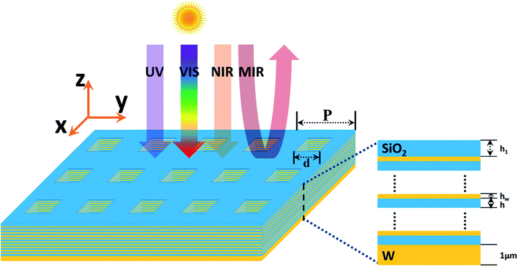
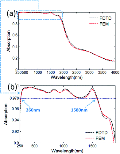
Here, we employ a nanoporous HMM structure to design the solar selective absorber, shown schematically in Fig. 1. In this work, W and SiO2 are chosen as the base materials of the solar absorber owing to their thermal stability at high temperatures.28,39 The nanopores of the structure are to reduce the effective refractive index of this absorber, which can achieve a better impedance match to free space. The first SiO2 layer coated onto the structure is operating as an antireflective material, which is to further reduce the impedance mismatch. The periods of the structure are chosen as 50 nm for both the x-direction and the y-direction, which is to ensure that this solar absorber is a sub-wavelength nanostructure. In addition, the W have a high reflection in infrared region, and hence the structure also will be a good reflector at the infrared region, in which the incident wavelength is much larger than the period of the nanostructure. The thickness of the W substrate is much larger than the radiation penetration depth, which can eliminate all transmission of incident light. Therefore, we take transmission(T) as zero, and the frequency-dependent absorption of this structure can be indirectly given by A = 1 − R, where A and R represent the absorption and reflection, respectively. Then, considering the reliability and precision of the calculated results, the absorptivity spectrum of the designed absorber is numerically calculated by finite element method (FEM) and finite-difference time-domain(FDTD) method respectively. The FEM calculation is performed using the commercial software COMSOL MULTIPHYSICS. In this simulation, the optical properties of W and SiO2 are obtained from ref. 66. The boundary conditions are set to be periodic in x and y direction, and a perfect matching layer boundary condition is applied in the z direction. If a plane wave is incident at the incidence angles, the Bloch boundary conditions are applied in both x and y directions. TM polarization is defined as the magnetic field is parallel with x-direction, and TE polarization is defined as the electric field parallel with x-direction. The optimum parameters of the proposed structure with 15 W/SiO2 layers are as follows: the period(P = 50 nm), the thickness of W layers (hw = 10 nm), the thickness of SiO2 layers (h = 50 nm), the thickness of first SiO2 layer (h1 = 60 nm), and the width of nanopores (d = 40 nm).The absorption spectrum of the proposed structure is shown in Fig. 2(a), which clearly shows a highly selective characteristic spanning from UV to infrared range. The same calculation results of absorption spectrum are obtained by using the FDTD and the FEM, respectively. According to the local enlarged drawing of the absorption spectra shown in Fig. 2(b), the absorption is close to unity in the UV, visible and NIR region. The average absorption can reach as high as 98.95% over the wavelength range of 260 to 1580 nm, which significantly exceed most of previously reported metamaterial solar absorbers both in the efficiency and bandwidth of solar absorption.6,12–26,36–65 The proposed solar absorber are numerically demonstrated to possess a near perfect absorption in the UV region from 250 to 400 nm. At the same time, the mid-infrared absorption is decreased significantly, which is remarkably beneficial for the improvement of the total photothermal conversion efficiency.
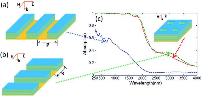
As shown in Fig. 3a and b, the proposed structure can be divided into two individual parts: (i) the HMM waveguide arrays with electric field along direction perpendicular to the W/SiO2 waveguide, which is periodic in the x-direction and extends to infinity in the y-direction; and(ii) the HMM waveguide arrays with electric field along direction parallel to the W/SiO2 waveguide, which is periodic in the y-direction and extends to infinity in the x-direction. In most of previously published studies about the absorbers based on HMM waveguide arrays, the absorbers with electric field along the direction perpendicular to metal/dielectric waveguide can achieve a high absorption over a wide spectral range, and the absorption performance of absorbers will be significantly deteriorated for electric field along direction parallel to metal/dielectric waveguide.27–34 These features widely exist in previously reported HMM waveguide taper arrays or sawtooth anisotropic metamaterial absorber, and the high absorption in these previous works have already been interpreted with slow-light effect detailly.27–34 However, as shown in Fig. 3(c), it is interesting to note that, the HMM waveguide arrays depicted in Fig. 3(b) possess an efficient and ultra-broadband solar absorption, and meanwhile the absorption performance of the HMM waveguide arrays depicted in Fig. 3(a) is obviously degraded, which shows an phenomenon being absolutely different from those in previously published studies about HMM waveguide array absorbers. Clearly, in this work, the HMM waveguide arrays, with electric field along direction parallel to metal/dielectric waveguide, play a major role in the absorption enhancement of the original proposed absorber. Therefore, compared with the conventional tapered HMM (or sawtooth anisotropic metamaterial) absorbers,27–34 which is related to the slow-light effect, our nanoporous HMM structures may have a completely different absorption mechanism.
In order to elucidate the physical mechanism of this proposed solar absorber, we investigate distributions of the magnetic field (|Hy|) along plane α at seven different wavelengths for the TM polarized incident light, respectively. According to the magnetic field distributions in Fig. 4, it is found that the magnetic polaritons are excited at the metal/dielectric interfaces. With increasing the wavelength of incident light, the magnetic resonances located in upper metal/dielectric interfaces become weaker, but the magnetic resonances located in lower metal/dielectric interfaces are enhanced with increasing operating wavelength. Therefore, the absorption in shorter wavelengths is mainly caused by the magnetic resonances located in upper metal/dielectric interfaces, and the absorption in longer wavelengths mainly caused by the magnetic resonances located in lower metal/dielectric interfaces,68 which have no relations with the slow-light effect. Clearly, the magnetic field distributions of this designed absorber are significantly different from those of these reported absorbers related to slow-light effect,27–34 which agrees well with the analysis results of Fig. 3. As shown in Fig. 5, we also investigate the magnetic field (|Hy|) distributions along β plane at six different wavelengths. The magnetic field is clearly located in the metal/dielectric interfaces of the multi-layer strip parallel to the direction of electric polarization, indicating that the efficient absorption of the proposed structure mainly caused by the multi-layer strip parallel to the direction of electric polarization, which is also in line with the calculated results in Fig. 3. Thus, the efficient solar absorption of our nanoporous HMM structures mainly caused by magnetic resonance, which have a completely different absorption mechanism to the conventional tapered HMM absorbers associated with the slow-light effect.27–34
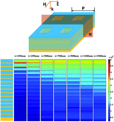 | ||
| Fig. 4 Spatial distribution of magnetic field (Hy) along plane α in the x–z plane at different wavelengths. | ||
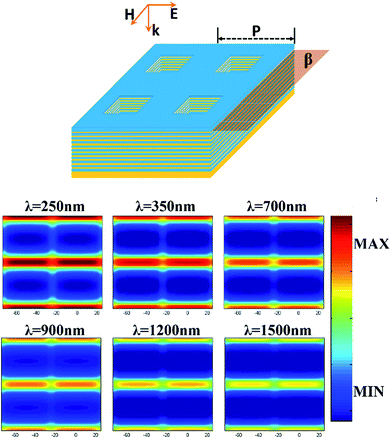 | ||
| Fig. 5 Spatial distribution of magnetic field (Hy) along plane β in the x–y plane at different wavelengths. | ||
To further understand the physical mechanism of the metamaterial absorber, we also analyze the y-component electric field (Ey) and the z-component electric field (Ez) at the metal/dielectric interface the plane β (we choose wavelength λ0 = 250 nm as an example). As shown in Fig. 6, the electric fields are strongly localized at the edges of the metal film, which indicates the excitation of electric dipole resonances.30 The electric dipolar resonances are due to localized surface plasmon resonance(LSPR) caused by the opposite charges accumulated at the edges of the metal film.30 Consequently, magnetic polaritons are formed, which cause strong magnetic resonance shown in Fig. 4 and 5. Therefore, these field localizations indicate that the nanoporous metamaterial structures could support LSPR effects to confine and then absorb the incident light.
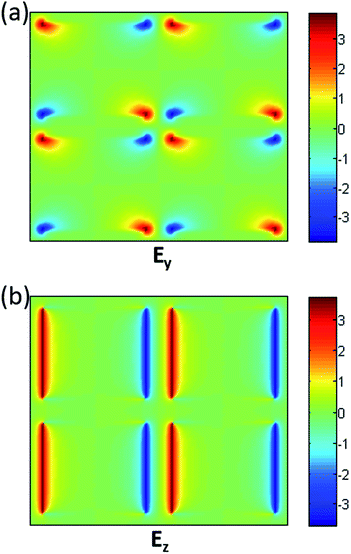 | ||
| Fig. 6 Distributions of (a) the y-component electric field (Ey); (b) the z-component electric field (Ez) at the metal/dielectric interface (β plane), when the wavelength λ0 = 250 nm. | ||
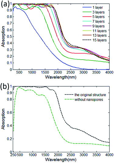
To better understand the nature of this efficient solar absorber, the absorption spectra of (i) the designed nanoporous metamaterials with various number of W/SiO2 layer, and (ii) the designed metamaterial structure without nanopores are investigated, respectively. As shown in Fig. 7(a), we give examples of tuning the absorption spectra by varying the numbers of W/SiO2 pairs. Clearly, the number of W/SiO2 pairs play important roles on the absorption spectrum. By stacking the W/SiO2 layers, an ultra-broadband absorber with near-perfect absorption at the whole solar spectrum can be formed. It can be seen that these FDTD/FEM modelled results are in good agreement with the analyses of magnetic distributions in Fig. 4, in which the efficient absorption at the shorter wavelength is caused by the magnetic resonance located in upper position and the W/SiO2 layers in lower position is helpful for achieving a broadband near-perfect absorption at the longer wavelength. Then, considering the demands of industrial applications, for the ideal cut-off solar absorbers operating in relatively low temperatures, a larger values of λcut-off are required to achieve a high total solar thermal energy conversion efficiency. However, the ideal values of λcut-off should decrease gradually with an increase of the operating temperature for reducing the radiative heat loss, which is very important for the improvement of total solar thermal conversion. Thus, according to Fig. 7(a), it is interesting to observe that the optical properties of the proposed absorbers can be easily controlled by changing the number of W/SiO2 layers, which indicates that we can use the solar absorbers in different temperatures for various applications. Besides, from Fig. 7(b), the structure with nanopores also can achieve a better absorption than the structure without nanopores. This can be understood by that the nanopores of the structure make the incident lights much easier to enter the solar absorber without being reflected owing to impedance matching.
The common rule for achieving a wider absorption band is to broaden the operating band with the impedance matching between absorbers and air. In order to better understand the behaviours of the near-perfect and broadband absorption shown in Fig. 7, we also give a detailed calculation based on the impedance matching method. To analyse the impedance matching condition, an effective medium theory is utilized. The relation between S parameters and impedance Z can be calculated by:67
 | (1) |
 | (2) |
 | (3) |
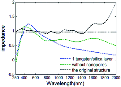
The relationship between the effective impedance Z of the original structure with 15 W/SiO2 layers and wavelength λ is plotted in Fig. 8. Then, the impedance of the free space is calculated by  . Clearly, the real part of effective impedance is close to one at the wavelength range of 260–1580 nm, which is very consistent with the broad wavelength band with near-perfect absorption shown in Fig. 2(b). Besides, as shown in Fig. 8, the impedance curve of the designed nanostructure without W/SiO2 layers as a function of wavelength λ are depicted, and the impedance curve of the designed nanostructure with 1 W/SiO2 layer as a function of wavelength λ are also calculated, which is in line with the absorption spectra shown in Fig. 7, respectively.
Owing to the random nature of solar radiation, the polarization insensitive performance of solar absorbers is important in practical applications. The absorption performance of the proposed solar absorbers with various polarization directions are calculated and depicted in Fig. 9(a), which shows that the proposed solar absorber is polarization-insensitive owing to the four-fold rational symmetrical structure. Besides, the absorption performance of this structure is mainly determined by the following geometrical parameters: (i) side length of the nanopores d; (ii) thickness of antireflective SiO2 layer h1; (iii) thickness of SiO2 layer h. Then, to show the effect of geometrical dimensions on the absorption performance, we calculate the absorption spectra of the selective solar absorbers at various d, h1 or h values, respectively. Other parameters of this absorber are fixed. According to Fig. 9(b), the solar absorber with a larger pore-sized porous can achieve a wider band of high absorption, which can be explained by that the relative low effective index and the small impedance mismatch of large pore-sized porous structures will enhance the absorption at longer wavelengths. On the contrary, when the size of the nanopores is much smaller than the wavelength of the light, the narrower absorption is mainly caused by the magnetic resonance in the first W/SiO2 interface, because very little light can propagate into the designed structure. As shown in Fig. 9(c), solar absorption increases slightly with an increase in the first SiO2 thickness. Besides, the dependence of absorption performance on the h1 was small when the first SiO2 layer is sufficiently thick, which is helpful for fabricating owing to the insensitivity to the film thickness. As shown in Fig. 9(d), the increase of thickness can further enhance the absorption at the long wavelengths, which means the change of the cut-off absorption frequency of selective solar absorbers. Clearly, from the calculated results shown in Fig. 7(a) and 9(d), the bandwidth and cut-off absorption frequency of absorbers can be finely tuned by the geometrical dimensions and pore size of nanoporous structures. This is important for many applications such as thermophotovoltaics.
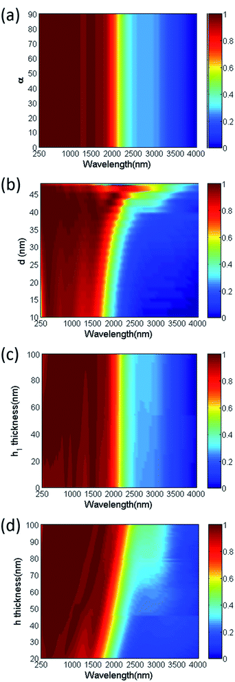 | ||
| Fig. 9 Spectral normal absorption contour plot for various (a) polarization angles (b) side of nanopores d (c) thicknesses h1 of first SiO2 layer (d) thicknesses h of SiO2 layers. | ||
One of major challenges in developing efficient light absorbers for solar energy applications is to find an efficient solar absorption mechanism working covering broad spectral and angular domains. Then, as shown in Fig. 10, we calculate the angular dependency of the absorption spectrum of the proposed solar absorber for both TE and TM configurations, respectively. Clearly, for the TM case, the properties of selective efficient solar absorption are nearly independent of incident angles, and for the case of TE polarization, the broadband absorption maintains almost did not change for the angles in the range of ±50°, which indicates the wide-angle absorption of the nanoporous structures. However, there is a slightly decrease in the absorption and bandwidth for the incident angle of 60° at TE polarization, because the magnetic resonances cannot be efficiently stimulated with the increasing of the incident angles. But, in this case, the high average solar absorption above 90% and the spectrally selectivity are still well maintained. Therefore, all these calculated results reveal that our proposed structure can produce a wide-angle polarization-insensitive and efficient selective solar absorption with wide angular response for both TE and TM configurations.
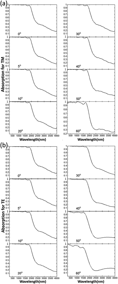 | ||
| Fig. 10 The calculated absorption spectra in the wavelength range of 250–4000 nm at various incident angles (0–60 degrees) for (a) TM-polarized light and (b) TE-polarized light. | ||
To quantify the performance to convert sunlight into heat, the total photothermal conversion efficiency of the proposed selective solar absorber can be defined by:6,15
 | (4) |
 | (5) |
 | (6) |
| Absorber type | Operating conditions | η |
|---|---|---|
| Ideal cut-off absorber | 373.15 K | 0.9560 |
| The absorber with 15 W/SiO2 layers | 373.15 K | 0.9032 |
| The absorber with 3 W/SiO2 layers | 373.15 K | 0.8860 |
| The absorber with 1 W/SiO2 layers | 373.15 K | 0.8550 |
| Ideal cut-off absorber | 1000 K | 0.9213 |
| The absorber with 15 W/SiO2 layers | 1000 K | 0.8253 |
| The absorber with 3 W/SiO2 layers | 1000 K | 0.8265 |
| The absorber with 1 W/SiO2 layers | 1000 K | 0.8157 |
| Ideal cut-off absorber | 1300 K | 0.8465 |
| The absorber with 15 W/SiO2 layers | 1300 K | 0.7251 |
| The absorber with 3 W/SiO2 layers | 1300 K | 0.7531 |
| The absorber with 1 W/SiO2 layers | 1300 K | 0.7647 |
3 Conclusions
In conclusion, we employ a nanoporous hyperbolic metamaterial with multiple W/SiO2 layers to design an efficient solar absorber, which can realize an average solar absorption as high as 98.9% in the wavelength range of 260–1580 nm. And meanwhile a low emissivity can be achieved in the mid-IR regime. Therefore, this structure can effectively convert solar energy into heat, while avoiding thermal radiation in the mid-IR regime, which lead to a superior total photothermal performance. The present work also clearly shows the difference of the absorption mechanism on this designed nanoporous HMM from those reported multi-layer nanostructures. Unlike the conventional tapered HMM (or sawtooth anisotropic metamaterial) absorbers, which is related to the slow-light effect, the design of solar absorbers in this work is quite helpful in the formation of impedance matching as well as magnetic resonance generated by LSPR, and thus can reduce the reflection as well as greatly enhance the absorption of incident light over an ultra-broad spectral range. In additional, in terms of producing technology, the nontapered structure can be easier to fabricate. A detailed numerical study is also performed for various polarizations and incident angles, which indicate that this solar absorber is polarization and angle independent. Especially the average solar absorption above 90% is also maintained for incident angles up to 60° at both TM and TE polarizations. In addition, by changing the number of W/SiO2 layers or the length of the side of nanopores, the λcut-off can be tuned to maximize the total photothermal conversion efficiency under different operating temperatures, which make the proposed absorbers very useful in a wide variety of practical applications. Due to the attractive properties such as near-unity absorption, broadband operation, wide angle, polarization-independence, spectral selectivity and high tunability, the proposed absorber displays widely promising applications in many fields of solar energy.Conflicts of interest
There are no conflicts to declare.Acknowledgements
National Key R&D Program of China (2016YFA0301300); National Natural Science Foundation of China (NSFC) (61275201, 61372037); Beijing Excellent PhD Thesis Guidance Foundation (20131001301); BUPT Excellent PhD Students Foundation (CX2017401).References
- D. M. Bierman, A. Lenert, W. R. Chan, B. Bhatia, I. Celanović, M. Soljačić and E. N. Wang, Nat. Energy, 2016, 1, 16068 CrossRef.
- G. Ni, G. Li, S. V. Boriskina, H. Li, W. Yang, T. Zhang and G. Chen, Nat. Energy, 2016, 1, 16126 CrossRef.
- X. Hu, W. Xu, L. Zhou, Y. Tan, Y. Wang, S. Zhu and J. Zhu, Adv. Mater., 2017, 29, 201604031 Search PubMed.
- A. Lenert, D. M. Bierman, Y. Nam, W. R. Chan, I. Celanović, M. Soljačić and E. N. Wang, Nat. Nanotechnol., 2015, 9, 126 CrossRef PubMed.
- L. Zhou, Y. Tan, J. Wang, W. Xu, Y. Yuan, W. Cai, S. Zhu and J. Zhu, Nat. Photonics, 2016, 10, 393–398 CrossRef.
- I. E. Khodasevych, L. Wang, A. Mitchell and G. Rosengarten, Adv. Opt. Mater., 2015, 3, 852–881 CrossRef.
- H. Zhu and F. Yi, Nat. Photonics, 2016, 10, 709–714 CrossRef.
- L. Zhou, Y. Tan, D. Ji, B. Zhu, P. Zhang, J. Xu, Q. Gan, Z. Yu and J. Zhu, Sci. Adv., 2016, 2, e1501227 Search PubMed.
- Y. Hu, S. Si, A. Mei, Y. Rong, H. Liu, X. Li and H. Han, Sol. RRL, 2017, 1, 201600019 Search PubMed.
- Q. Fan, W. Su, X. Meng, X. Guo, G. Li, W. Ma, M. Zhang and Y. Li, Sol. RRL, 2017, 1, 1700020 CrossRef.
- S. J. Kim, P. Fan, J. Kang and M. L. Brongersma, Nat. Commun., 2015, 6, 7591 CrossRef PubMed.
- K. Lin, H. Chen, Y. Lai, C. Yu, Y. Lee, P. Su, Y. Yen and B. Chen, Nano Energy, 2017, 37, 61–73 CrossRef.
- D. Liu and Q. Li, Sub-nanometer planar solar absorber, Nano Energy, 2017, 34, 172–180 CrossRef.
- D. Wu, C. Liu, Y. Liu, L. Yu, Z. Yu, L. Chen, R. Ma and H. Ye, Opt. Lett., 2017, 42, 450 CrossRef PubMed.
- V. Rinnerbauer, A. Lenert, D. M. Bierman, Y. X. Yeng, W. R. Chan, R. D. Geil, J. J. Senkevich, J. D. Joannopoulos, E. N. Wang, M. Soljačić and I. Celanovic, Adv. Energy Mater., 2014, 4, 3412–3420 Search PubMed.
- D. Wu, Y. Liu, Z. Xu, Z. Yu, L. Yu, L. Chen, C. Liu, R. Li, R. Ma, J. Zhang and H. Ye, Sol. RRL, 2017, 1, 1700049 CrossRef.
- A. Datas and A. Martí, Sol. Energy Mater. Sol. Cells, 2017, 161, 285–296 CrossRef.
- Y. Nam, Y. X. Yeng, A. Lenert, P. Bermel, I. Celanovic, M. Soljačić and E. N. Wang, Sol. Energy Mater. Sol. Cells, 2014, 122, 287–296 CrossRef.
- K. J. Berean, V. Sivan, I. Khodasevych, A. Boes, E. D. Gaspera, M. R. Field, K. K. Zadeh, A. Mitchell and G. Rosengarten, Adv. Opt. Mater., 2016, 4, 1247–1254 CrossRef.
- J. Yan, P. Liu, C. Ma, Z. Lin and G. Yang, Nanoscale, 2016, 8, 8826 RSC.
- R. Komatsu, A. Balčytis, G. Seniutinas, T. Yamamura, Y. Nishijima and S. Juodkazis, Sol. Energy Mater. Sol. Cells, 2015, 143, 72–77 CrossRef.
- H. Wang, Q. Chen, L. Wen, S. Song, X. Hu and G. Xu, Photonics Res., 2015, 3, 329 CrossRef.
- Z. J. Coppens, I. I. Kravchenko and J. G. Valentine, Adv. Opt. Mater., 2016, 4, 5 Search PubMed.
- D. Wu, Y. Liu, L. Yu, Z. Yu, L. Chen, R. li, R. Ma, C. Liu, J. Zhang and H. Ye, Sci. Rep., 2017, 7, 45210 CrossRef PubMed.
- Y. Cui, K. H. Fung, J. Xu, H. Ma, Y. Jin, S. He and N. X. Fang, Nano Lett., 2012, 12, 1443 CrossRef PubMed.
- A. Tittl, M. G. Harats, R. Walter, X. Yin, M. Schäferling, N. Liu, R. Rapaport and H. Giessen, ACS Nano, 2014, 8, 10885 CrossRef PubMed.
- J. Zhou, A. F. Kaplan, L. Chen and L. J. Guo, ACS Photonics, 2014, 1, 618–624 CrossRef.
- P. N. Dyachenko, S. Molesky, A. Yu Petrov, M. Störmer, T. Krekeler, S. Lang, M. Ritter, Z. Jacob and M. Eich, Nat. Commun., 2016, 7, 11809 CrossRef PubMed.
- B. X. Wang, C. Y. Zhao, X. Fang and Y. H. Kan, Opt. Lett., 2017, 42, 1879–1882 CrossRef PubMed.
- Q. Liang, T. Wang, Z. Lu, Q. Sun, Y. Fu and W. Yu, Adv. Opt. Mater., 2013, 1, 43–49 CrossRef.
- Q. Liang, W. Yu, W. Zhao, T. Wang, J. Zhao, H. Zhang and S. Tao, Opt. Mater. Express, 2013, 3, 1187–1196 CrossRef.
- D. Ji, H. Song, X. Zeng, H. Hu, K. Liu, N. Zhang and Q. Gan, Sci. Rep., 2014, 4, 4498 CrossRef PubMed.
- M. Sakhdari, M. Hajizadegan, M. Farhat and P. Chen, Nano Energy, 2016, 26, 371–381 CrossRef.
- Y. Lin, Y. Cui, F. Ding, K. H. Fung, T. Ji and D. Li, Opt. Mater. Express, 2017, 7, 606–617 CrossRef.
- L. Zhou, S. Zhuang, C. He, Y. Tan, Z. Wang and J. Zhu, Nano Energy, 2017, 32, 195–200 CrossRef.
- J. Geldmeier, T. König, M. A. Mahmoud, M. A. El-Sayed and V. V. Tsukruk, Adv. Funct. Mater., 2015, 24, 6797–6805 CrossRef.
- K. Aydin, V. E. Ferry, R. M. Briggs and H. A. Atwater, Nat. Commun., 2011, 2, 517 CrossRef PubMed.
- C. Wan, Y. Ho, S. Nunez-Sanchez, L. Chen, M. Lopez-Garcia, J. Pugh, B. Zhu, P. Selvaraj, T. Mallick, S. Senthilarasu and M. J. Cryan, Nano Energy, 2016, 26, 392–397 CrossRef.
- H. Wang, V. P. Sivan, A. Mitchell, G. Rosengarten, P. Phelan and L. Wang, Sol. Energy Mater. Sol. Cells, 2015, 137, 235–242 CrossRef.
- L. P. Wang and Z. M. Zhang, Appl. Phys. Lett., 2012, 100, 063902 CrossRef.
- M. Bilokur, A. Gentle, M. D. Arnold, M. B. Cortie and G. B. Smith, Solar RRL, 2017, 1, 1700092 CrossRef.
- N. H. Thomas, C. Zhen, S. Fan and A. J. Minnich, Sci. Rep., 2017, 7, 5362 CrossRef PubMed.
- P. Li, B. Liu, Y. Ni, K. K. Liew, J. Sze, S. Chen and S. Shen, Adv. Mater., 2015, 27, 4585 CrossRef PubMed.
- H. Wang and L. Wang, Perfect selective metamaterial solar absorbers, Opt. Express, 2013, 6, A1078 CrossRef PubMed.
- J. Song, H. Wu, Q. Cheng and J. Zhao, J. Quant. Spectrosc. Radiat. Transfer, 2015, 158, 136–144 CrossRef.
- W. Li, U. Guler, N. Kinsey, G. V. Naik, A. Boltasseva, J. Guan, V. M. Shalaev and A. V. Kildishev, Adv. Mater., 2014, 26, 7921 CrossRef.
- J. W. Yoon, K. J. Lee, W. Wu and R. Magnusson, Adv. Opt. Mater., 2015, 2, 1206–1212 CrossRef.
- X. Fang and C. Y. Zhao, Int. J. Heat Mass Transfer, 2017, 111, 1098–1106 CrossRef.
- D. Liu, H. Yu, Z. Yang and Y. Duan, Nano Res., 2016, 9, 2354–2363 CrossRef.
- A. Xianyu, W. Xuyue, Y. Guanbo, D. Kangkang, X. Yali and H. Sailing, Small, 2015, 11, 1526–1530 CrossRef PubMed.
- M. Hong, S. A. Maier, X. Luo, X. Li and Y. Chen, Photonics Res., 2015, 3, 54–57 CrossRef.
- D. M. Nguyen, D. Lee and J. Rho, Sci. Rep., 2017, 7, 2611 CrossRef PubMed.
- Y. Cui, Y. He, Y. Jin, F. Ding, L. Yang, Y. Ye, S. Zhong, Y. Lin and S. He, Laser Photonics Rev., 2014, 8, 495–520 CrossRef.
- F. Ding, Y. Jin, B. Li, H. Cheng, L. Mo and S. He, Laser Photonics Rev., 2013, 8, 946–953 CrossRef.
- Z. Li, E. Palacios, S. Butun, H. Kocer and K. Aydin, Sci. Rep., 2015, 5, 15137 CrossRef PubMed.
- C. Ng, J. Cadusch, S. Dligatch, A. Roberts, T. J. Davis, P. Mulvaney and E. G. Daniel, ACS Nano, 2016, 10, 4704 CrossRef PubMed.
- M. K. Hedayati, M. Javaherirahim, B. Mozooni, R. Abdelaziz, A. Tavassolizadeh, V. S. Chakravadhanula, V. Zaporojtchenko, T. Strunkus, F. Faupel and M. Elbahri, Adv. Mater., 2011, 23, 5410 CrossRef PubMed.
- I. Khan, H. Keshmiri, F. Kolb, T. Dimopoulos, E. J. W. List-Kratochvil and J. Dostalek, Adv. Opt. Mater., 2016, 4, 435–443 CrossRef.
- J. Y. Lu, S. H. Nam, K. Wilke, A. Raza, Y. E. Lee, A. Alghaferi, Y. E. Lee, A. AlGhaferi, N. X. Fang and T. Zhang, Adv. Opt. Mater., 2016, 4, 1255–1264 CrossRef.
- B. H. Wu, W. T. Liu, T. Y. Chen, T. P. Perng, J. H. Huang and L. J. Chen, Nano Energy, 2016, 27, 412–419 CrossRef.
- F. Tan, N. Wang, D. Y. Lei, W. Yu and X. Zhang, Adv. Opt. Mater., 2017, 5, 201600399 Search PubMed.
- S. Ishii, K. Chen, H. Okuyama and T. Nagao, Adv. Opt. Mater., 2017, 5, 1600902 CrossRef.
- C. Hägglund, G. Zeltzer, R. Ruiz, A. Wangperawong, K. Roelofs and S. F. Bent, ACS Photonics, 2016, 3, 456–463 CrossRef.
- L. Zhou, Y. Zhou, Y. Zhu, X. Dong, B. Gao, Y. Wang and S. Shen, J. Mater. Chem. C, 2015, 4, 391–397 RSC.
- Z. Liu, X. Liu, S. Huang, P. Pan, J. Chen, G. Liu and G. Gu, ACS Appl. Mater. Interfaces, 2015, 7, 4962–4968 Search PubMed.
- E. D. Palik, Handbook of Optical Constants of Solids, Academic press, San Diego,CA, 1998 Search PubMed.
- D. R. Smith, D. C. Vier, T. Koschny and C. M. Soukoulis, Phys. Rev. E: Stat., Nonlinear, Soft Matter Phys., 2005, 71, 036617 CrossRef PubMed.
- J. Chen, P. Wang, Z. M. Zhang, Y. Lu and H. Ming, Phys. Rev. E: Stat., Nonlinear, Soft Matter Phys., 2011, 84, 026603 CrossRef PubMed.
- Air Mass 1.5 Spectra, American Society for Testing and Materials(ASTM). Available from: http://rredc.nrel.gov/solar/spectra/am1.5/.
| This journal is © The Royal Society of Chemistry 2018 |

