 Open Access Article
Oxygen insensitive thiol–ene photo-click chemistry for direct imprint lithography of oxides†
Ravikiran Nagarjunaa,
Mohammad S. M. Saifullahb and
Ramakrishnan Ganesan *a
*a
aDepartment of Chemistry, Birla Institute of Technology and Science (BITS) Pilani, Hyderabad Campus, Jawahar Nagar, Shameerpet Mandal, Hyderabad, 500078, India. E-mail: ram.ganesan@hyderabad.bits-pilani.ac.in
bInstitute of Materials Research and Engineering, A*STAR (Agency for Science, Technology, and Research), 2 Fusionopolis Way, #08-03 Innovis, Singapore 138634, Republic of Singapore
First published on 22nd March 2018
Abstract
UV-nanoimprint lithography (UV-NIL) is a promising technique for direct fabrication of functional oxide nanostructures. Since it is mostly carried out in aerobic conditions, the free radical polymerization during imprinting is retarded due to the radical scavenging ability of oxygen. Therefore, it is highly desirable to have an oxygen-insensitive photo-curable resin that not only alleviates the requirement of inert conditions but also enables patterning without making substantial changes in the process. Here we demonstrate the formulation of metal-containing resins that employ oxygen-insensitive thiol–ene photo-click chemistry. Allyl acetoacetate (AAAc) has been used as a bifunctional monomer that, on one hand, chelates with the metal ion, and on the other hand, offers a reactive alkene group for polymerization. Pentaerythritol tetrakis(3-mercaptopropionate) (PETMP), a four-arm thiol derivative, is used as a crosslinker as well as an active component in the thiol–ene photo-click chemistry. The FT-IR analyses on the metal-free and metal-containing resin formulations revealed that the optimum ratio of alkene to thiol is 1![[thin space (1/6-em)]](https://www.rsc.org/images/entities/char_2009.gif) :
:![[thin space (1/6-em)]](https://www.rsc.org/images/entities/char_2009.gif) 0.5 for an efficient photo-click chemistry. The thiol–ene photo-click chemistry has been successfully demonstrated for direct imprinting of oxides by employing TiO2 and Ta2O5 as candidate systems. The imprinted films of metal-containing resins were subjected to calcination to obtain the corresponding patterned metal oxides. This technique can potentially be expanded to other oxide systems as well.
0.5 for an efficient photo-click chemistry. The thiol–ene photo-click chemistry has been successfully demonstrated for direct imprinting of oxides by employing TiO2 and Ta2O5 as candidate systems. The imprinted films of metal-containing resins were subjected to calcination to obtain the corresponding patterned metal oxides. This technique can potentially be expanded to other oxide systems as well.
1. Introduction
Due to its simplicity, versatility, and specific reactivity, click chemistry has gained significant interest in various fields including organic transformations, surface functionalization, polymeric materials, and biological applications.1–6 Several reactions including alkyne–azide, Diels–Alder reactions, thiol–ene, thiol–yne, etc., have been classified under click chemistry, as these reactions directly yield an adduct without giving any other byproduct.7 Among them, thiol–ene click is an interesting reaction occurring between commonly available reactive alkenes and thiol groups, which is known to be tolerant to the presence of oxygen and moisture when the oxygen concentration is less than that of thiol.8–12 Thiol–ene reaction is also called as hydrothiolation, in which the thiol group adds across the carbon–carbon double bond in anti-Markovnikov orientation. Generally, the hydrothiolation reaction can proceed under a variety of conditions such as thermal catalytic processes, and photo-addition.13–16 Hydrothiolation via photo-clicking is attractive as it proceeds well at room temperature reaction conditions. In a typical thiol–ene click reaction, the photo-generated electron from a photo-initiator is transferred to the thiol group to produce a thiyl radical, which adds across a carbon–carbon double bond and thus transferring the radical to the alkene. Abstraction of a hydrogen radical from the neighborhood thiol to this carbon radical accomplishes the hydrothiolation, while simultaneously propagating the chain reaction.9,17Fabrication of micro/nanostructures of oxides is of paramount importance in various applications including photoelectrochemical cells,18 photovoltaic cells,19 sensors,20 and catalysis.21 Several techniques including photolithography,22,23 electron-beam lithography,24,25 electro-hydrodynamic lithography,26,27 direct write assembly,28 selective surface wetting,29 dip-pen nanolithography,30,31 nanoimprint lithography (NIL)32–34 among others35,36 have been utilized towards fabrication of metal oxide micro/nanostructures. Each of these techniques has its own merits as well as limitations. Among the various available techniques, NIL has been regarded as the next generation fabrication approach due to its advantages such as simplicity, low-cost, high-fidelity, high-resolution, non-dependence on the optical diffraction limit, compatibility with various substrates and ability to imprint arbitrary structures over flat and curved surfaces.37–40 The descendants of NIL like step-and-flash,41–43 roll-to-roll44 and roll-to-flat45 imprint lithography techniques have augmented its high-throughput capability while maintaining high-precision. The NIL process can be broadly classified into two categories: thermal and UV. Thermal NIL requires temperature cycling, which reduces the throughput, affects the mold life, and leads to line-width variation owing to the differences in thermal expansion coefficients of the mold, substrate, and resist.46 On the other hand, UV-NIL is an attractive room temperature process that does not require any temperature cycling, and thereby allows high-throughput patterning.
As opposed to the fabrication of polymeric micro/nanostructures, fabrication of oxides has inherent challenges in the materials design as the metal-containing polymers and ceramics do not possess workable characteristics for direct patterning. Therefore, the material design has to be customized as per the requirement of each technique. In the case of nanoimprinting, sol–gel approach was initially employed that utilized hydrolysis followed by condensation of metal alkoxides or halides.33,47–49 The conventional sol–gel approach suffered low yield due to the lack of mechanical strength of the imprints during the demolding step. Nanoparticle suspensions have also been used for direct nanoimprinting with a soft PDMS mold.50 This approach has been used to directly fabricate three-dimensional structures of multicomponent oxides like indium tin oxide and nickel ferrite.51,52 Photosensitive ethylhexanoate-based oxide patterning has been reported that utilizes photo-breakable precursors rather than photo-curable monomers.34 Recently, polymerizable sol–gel approach (PSG) has emerged as a promising method for rapid direct nanoimprinting of a host of metal oxides such as TiO2, ZrO2, Hf2O5 amongst others.46,53,54 The PSG approach utilizes metal-methacrylate liquid precursors that undergo in situ thermal- or photo-induced free radical polymerization during the nanoimprinting step. One of the major advantages of this approach is the spin-coatable liquid phase metal-containing resin that can easily fill up the pattern features of the mold at near-ambient pressure due to capillary action. Polymerization solidifies the metal-containing precursor and decreases the surface energy to facilitate easy and clean demolding. This approach has been found to harness the advantages and obviates the limitations of the conventional sol–gel approach. The PSG approach has been shown to be suitable for high-throughput step-and-flash imprint lithography for various oxides55 and to synthesize supported oxide photo-catalysts.56,57 Despite the high potential, the PSG approach based on free radical polymerization of methacrylates is vulnerable to radical scavenging by oxygen that could affect the degree of polymerization, which in turn could effect on the quality of imprinting. This warrants purging/bubbling of inert gas into the metal-containing resin before patterning in order to eliminate any dissolved oxygen.
As thiol–ene click chemistry can fulfil the requirements such as oxygen-insensitivity, spin-coatability, and room temperature photo-crosslinking, it is deemed to be attractive for UV-NIL.58–60 This chemistry has recently been shown for its potential for imprinting polymeric structures over flat and curved surfaces.61 However, the merits of the thiol–ene photo-click chemistry have so far not been realized for oxide nanoimprinting. Here, we show the augmentation of the PSG approach by employing the oxygen-insensitive thiol–ene click chemistry towards fabrication of metal oxide micro/nanostructures (Scheme 1). The design of the photo-curable metal-containing resin, its photo-curability and patternability are discussed by choosing titanium alkoxide as the precursor to fabricate TiO2 nanostructures. TiO2 was chosen as the principal oxide candidate, as it is one of the most studied semiconducting oxides that possesses huge potential for various applications including energy, health, and environment.62–64 Finally, the thiol–ene approach was also studied for patterning Ta2O5 in order to ascertain its potential towards structuring other metal oxides.
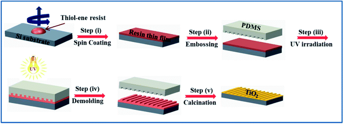 | ||
| Scheme 1 Schematic representation of the overall process involving thiol–ene click chemistry for imprinting of metal oxides. | ||
2. Experimental section
2.1 Materials and methods
Titanium(IV) isopropoxide, tantalum(V) ethoxide, allyl acetoacetate (AAAc), pentaerythritol tetrakis(3-mercaptopropionate) (PETMP), 2-(methacryloyloxy)ethyl acetoacetate (MAEAA), 2-hydroxy-2-methylpropiophenone (HMP), 1H,1H,2H,2H-perfluorodecyltrichlorosilane, and toluene were purchased from Sigma Aldrich and used as-received. Polydimethylsiloxane (PDMS) stamps were fabricated from Sylgard 184 purchased from Sigma Aldrich.2.2 Resin formulation
The TiO2 resists were prepared using requisite amounts of precursors as mentioned in Table 1. Briefly, one equivalent of Ti(i-PrO)4 was added and thoroughly stirred with 4 equivalents of AAAc in a glass vial inside a nitrogen glove box. The color of the solution rapidly turned into red that indicated the formation of Ti(AAAc)4 complex. To this complex, either half equivalent or one equivalent of the PETMP cross-linker was added and the resultant mixture was shaken well on a vortex stirrer for 2 min to obtain a clear solution. To this mixture, 3 wt% (with respect to the AAAc and PETMP) of HMP photo-initiator was added to formulate the imprintable resin, which was diluted with toluene in 1![[thin space (1/6-em)]](https://www.rsc.org/images/entities/char_2009.gif) :
:![[thin space (1/6-em)]](https://www.rsc.org/images/entities/char_2009.gif) 1 (wt/wt) ratio to decrease the viscosity. The Ta2O5 resist was also prepared in a similar manner by taking tantalum(V) ethoxide as the alkoxide source.
1 (wt/wt) ratio to decrease the viscosity. The Ta2O5 resist was also prepared in a similar manner by taking tantalum(V) ethoxide as the alkoxide source.
| Sample code | TIPO (mmol) | AAAc (mmol) | PETMP (mmol) | HMP (mmol) |
|---|---|---|---|---|
| TA | 1.0 | 4.0 | 0.0 | 0.156 |
| TAP-0.5 | 1.0 | 4.0 | 0.50 | 0.208 |
| TAP-1 | 1.0 | 4.0 | 1.00 | 0.277 |
2.3 Imprinting of metal oxide
First, PDMS stamps were fabricated following the standard procedure from Sylgard 184. Briefly, the silicon rubber base pre-polymer and cross-linker of Sylgard 184 were thoroughly mixed in 10![[thin space (1/6-em)]](https://www.rsc.org/images/entities/char_2009.gif) :
:![[thin space (1/6-em)]](https://www.rsc.org/images/entities/char_2009.gif) 1 weight ratio and the resulting mixture was poured over polycarbonate master mold kept in a Petri dish. This assembly was degassed in a vacuum desiccator to remove any trapped air bubbles. The assembly was the subjected to 70 °C for 1 h to induce cross-linking of the precursor. Finally, the PDMS elastomeric stamp was peeled off from the master mold. The fabricated PDMS stamps were treated with 1H,1H,2H,2H-perfluorodecyltrichlorosilane for 5 h inside an evacuated desiccator in order to decrease the surface energy that facilitates easy demolding. The water contact angle of the fluorinated PDMS stamp was found to be ∼130° as opposed to 105° for freshly prepared PDMS, indicating the reduction in surface energy.
1 weight ratio and the resulting mixture was poured over polycarbonate master mold kept in a Petri dish. This assembly was degassed in a vacuum desiccator to remove any trapped air bubbles. The assembly was the subjected to 70 °C for 1 h to induce cross-linking of the precursor. Finally, the PDMS elastomeric stamp was peeled off from the master mold. The fabricated PDMS stamps were treated with 1H,1H,2H,2H-perfluorodecyltrichlorosilane for 5 h inside an evacuated desiccator in order to decrease the surface energy that facilitates easy demolding. The water contact angle of the fluorinated PDMS stamp was found to be ∼130° as opposed to 105° for freshly prepared PDMS, indicating the reduction in surface energy.
In a typical nanoimprinting process, the metal-containing resin solution was spin-coated over a silicon wafer (20 mm × 20 mm) at 1000 rpm for 45 s. The PDMS mold was then placed on top of the wet thin film and a slight pressure was applied. This assembly was subjected to UV irradiation with a Hg vapor lamp (125 W) for 20 min to induce crosslinking of the monomers. After UV exposure, the PDMS stamp was carefully demolded and the imprints were subjected to calcination at designated temperatures for 1 h to obtain metal oxide micro/nanostructures.
2.4 Characterization
The thiol–ene photoreaction was following using FT-IR spectrophotometer (JASCO FTIR 4200). TGA analyses were carried out using Shimadzu DTG-60 differential thermal analyzer in air atmosphere to follow the degradation profile and the residual oxide mass present in the metal-containing resins. XRD patterns of the thin film samples calcined at different temperatures were measured at a scan rate of 1° min−1 using Rigaku Ultima IV X-ray diffractometer equipped with Cu Kα (λ = 1.5418 Å). Diffuse reflectance spectroscopy analysis of the thin film samples calcined at different temperatures was performed using JASCO V-670 UV-visible spectrophotometer. The surface morphology of the imprints before and after calcination was characterized using a Carl-Zeiss ULTRA-55 field emission scanning electron microscope (FE-SEM).3. Results and discussion
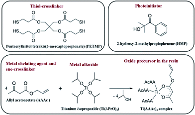
A judicious choice of precursors is the key to successful implementation of the thiol–ene click chemistry to realize oxide nanofabrication. In this regard, we chose pentaerythritol tetrakis(3-mercaptopropionate) (PETMP) as the cross-linker that has four thiol arms. Allyl acetoacetate (AAAc) was chosen as the bifunctional reagent that on one hand chelates with the metal center through the acetoacetate group and on the other hand possesses the reactive alkene group for the click reaction. When the metal center is chelated with more than one AAAc, it could also act as a cross-linker, which would lead to the formation of highly branched polymeric network. The chemical structures of the various components used in this study are shown in Fig. 1.To probe the thiol–ene click reaction under UV irradiation, we formulated a resin containing PETMP and AAAc in 1![[thin space (1/6-em)]](https://www.rsc.org/images/entities/char_2009.gif) :
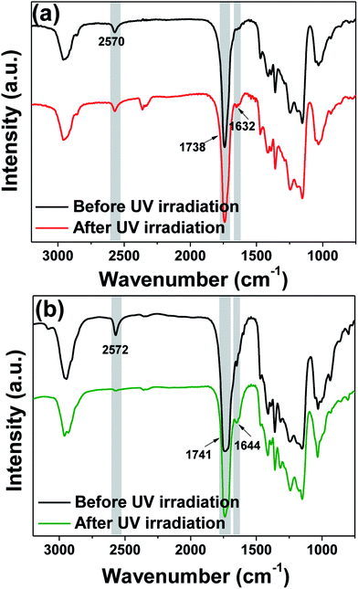
:![[thin space (1/6-em)]](https://www.rsc.org/images/entities/char_2009.gif) 4 ratio mixed with 3 wt% of 2-hydroxy-2-methylpropiophenone (HMP) photo-initiator. This metal-free resin was spin-coated over a pre-cleaned silicon wafer and studied with the Fourier transform infrared (FT-IR) spectroscopy to follow the thiol–ene photo-click chemistry (Fig. 2a). As seen from the figure, the characteristic –SH stretching peak was observed at 2570 cm−1, confirming the presence of free thiol groups in the resin formulation. In addition, an intense peak at 1738 cm−1 due to the carbonyl group stretching and a weak peak at 1632 cm−1 due to the alkene group were also observed. After subjecting the film to 20 min of UV irradiation, it remained wet, indicating poor efficiency of the thiol–ene click-reaction in this system. The FT-IR spectrum obtained after irradiation was almost identical to that before UV irradiation. We postulated that this could be due to the unfavorably positioned functional groups or reduced probability of stoichiometric encountering of the allyl and thiol groups in the thin film. Therefore, we decreased the amount of PETMP to half (PETMP and AAAc in 1
4 ratio mixed with 3 wt% of 2-hydroxy-2-methylpropiophenone (HMP) photo-initiator. This metal-free resin was spin-coated over a pre-cleaned silicon wafer and studied with the Fourier transform infrared (FT-IR) spectroscopy to follow the thiol–ene photo-click chemistry (Fig. 2a). As seen from the figure, the characteristic –SH stretching peak was observed at 2570 cm−1, confirming the presence of free thiol groups in the resin formulation. In addition, an intense peak at 1738 cm−1 due to the carbonyl group stretching and a weak peak at 1632 cm−1 due to the alkene group were also observed. After subjecting the film to 20 min of UV irradiation, it remained wet, indicating poor efficiency of the thiol–ene click-reaction in this system. The FT-IR spectrum obtained after irradiation was almost identical to that before UV irradiation. We postulated that this could be due to the unfavorably positioned functional groups or reduced probability of stoichiometric encountering of the allyl and thiol groups in the thin film. Therefore, we decreased the amount of PETMP to half (PETMP and AAAc in 1![[thin space (1/6-em)]](https://www.rsc.org/images/entities/char_2009.gif) :
:![[thin space (1/6-em)]](https://www.rsc.org/images/entities/char_2009.gif) 8 ratio) to provide more alkene double bonds per –SH group so as to enhance the probability of the reaction at the thiol group sites. Interestingly, the irradiated film became dry to yield a smooth photo-cured film. The FT-IR corresponding to this composition revealed the complete disappearance of the –SH stretching peak, strongly corroborating the occurrence of thiol–ene click reaction (Fig. 2b).
8 ratio) to provide more alkene double bonds per –SH group so as to enhance the probability of the reaction at the thiol group sites. Interestingly, the irradiated film became dry to yield a smooth photo-cured film. The FT-IR corresponding to this composition revealed the complete disappearance of the –SH stretching peak, strongly corroborating the occurrence of thiol–ene click reaction (Fig. 2b).
To enable the thiol–ene chemistry for oxide nanoimprinting, a photo-curable metal-containing resin formulation was prepared by mixing titanium-allyl acetoacetate complex [Ti(AAAc)4] with PETMP and HMP. Table 1 shows the three resin formulations that were used for photo-curability studies. The first composition (TA), which does not contain PETMP could undergo [2 + 2] photo-addition of alkene double bonds to yield cyclobutane derivative. This composition yielded a dry film after UV irradiation. However, the film was found to be brittle and easily flaked off of the silicon wafer. This could be due to the excessive photo-curing of the four-arm alkene-functionalized Ti(AAAc)4 that caused residual stress in the thin film.53 In the second composition (TAP-0.5), 1/8 equivalent of PETMP with respect to Ti(AAAc)4 was introduced to keep the effective available thiol groups per alkene as 0.5. This formulation after UV irradiation was found to yield a dry and smooth film that did not suffer any peeling off behavior. This could be attributed to the cushioning effect provided by the optimum cross-linking of PETMP that circumvented cracking of the film.
In the third composition (TAP-1), 1/4 equivalent of PETMP with respect to Ti(AAAc)4 was used in order to keep the thiol to alkene ratio 1![[thin space (1/6-em)]](https://www.rsc.org/images/entities/char_2009.gif) :
:![[thin space (1/6-em)]](https://www.rsc.org/images/entities/char_2009.gif) 1. Interestingly, the film obtained with this composition was found not fully dry after 20 min of UV irradiation. This is similar to the poor photo-curing observed with the metal-free resin containing stoichiometric ratio of allyl to thiol. Thus, for the remaining characterization and imprinting studies, we utilized the optimized composition of TAP-0.5.
1. Interestingly, the film obtained with this composition was found not fully dry after 20 min of UV irradiation. This is similar to the poor photo-curing observed with the metal-free resin containing stoichiometric ratio of allyl to thiol. Thus, for the remaining characterization and imprinting studies, we utilized the optimized composition of TAP-0.5.
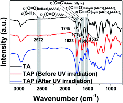
Fig. 3 shows the FT-IR analyses using TAP-0.5 to probe the thiol–ene photo-click reaction. As seen from the spectra, the characteristic ester and keto carbonyl groups are observed at 1745 and 1718 cm−1, respectively. Compared to the metal-free resin, pristine Ti(AAA)4 showed two additional characteristic peaks at 1610 and 1532 cm−1 that can be attributed to the bidendate chelation of the enol form of AAAc.54 In addition, the carbon–carbon double bond of allyl group appeared at 1633 cm−1. In the case of TAP-0.5, in addition to the above mentioned stretching peaks, a new peak at 2572 cm−1 corresponding to the thiol appeared. After UV light irradiation, the thiol peak became nearly invisible, while the intensity of allyl double bond peak diminished. These changes clearly indicate the occurrence of click reaction between the thiol and allyl groups in this system. It is noteworthy that the chelation with the metal remains intact even after the UV irradiation, which confirms that the metal is entrapped inside the cross-linked polymeric network.
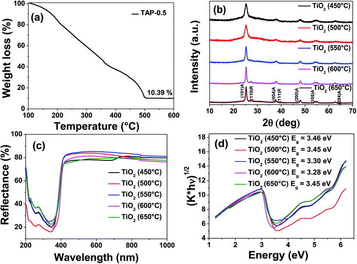
Fig. 4a shows the thermogravimetric analysis (TGA) of TAP-0.5 performed in air. A steady mass loss was observed between 100 and 500 °C due to the removal of residual solvent, low molecular weight monomers, and polymers. No further mass loss was observed above 500 °C, suggesting the complete removal of organics present in the resin. The residual inorganic mass corresponding to TiO2 at 500 °C was found to be 10.4% which is in close agreement with the theoretical estimated value of 11.9%.
To confirm the phases obtained after calcination of the UV-cured TAP-0.5 films, X-ray diffraction (XRD) and Raman spectroscopy were performed. The calcination temperature was varied from 450 to 650 °C at a constant duration of 1 h to monitor the evolution of the phases and the corresponding XRD patterns are presented in Fig. 4b. As seen from the figure, the TAP-0.5 films heat-treated at 450 and 500 °C revealed the formation of phase pure anatase. The broad peaks indicate the nanocrystalline nature of TiO2 obtained at these temperatures. Above 500 °C, the (101) anatase peak was found to intensify with narrowing of the peak, indicating the growth of nanocrystallites to larger crystals (JCPDS 89-4921). At and above 600 °C, formation of a small amount of rutile phase is indicated by the appearance of (110) plane at 2θ = 27.4°. Applying the Scherrer's formula to the (101) plane of anatase TiO2, the crystallite size of the samples calcined at 450, 500, 550, 600 and 650 °C are calculated to be 6.7, 7.1, 12.0, 15.7, and 15.6 nm, respectively. The Raman spectra of the TiO2 samples calcined at different temperatures looked identical (Fig. S4†). A major peak at 121 cm−1 along with weak peaks at 365, 482, and 603 cm−1 were observed in all cases that can be attributed to the respective vibrational symmetries of Eg, B1g, A1g, and Eg Raman-active modes of anatase TiO2.57,65 Due to the presence in minute quantity, the Raman peaks of rutile TiO2 were not observed in the samples calcined at 600 and 650 °C.
The semiconducting nature of the oxide thin films obtained through the thiol–ene approach has been studied using diffuse reflectance spectroscopy. The percentage reflectance and their corresponding Kubelka–Munk plots of TiO2 calcined at various temperatures are shown in Fig. 4c and d, respectively. The Kubelka–Munk factor (K) is given by K = (1 − R)2/2R, where R is the % reflectance. The intersection of the extrapolated linear portion of the curve in (K × energy)n versus energy plot with the energy axis yields the band gap of the semiconductor material. For direct band gap materials, the value of n is taken as 2, while for indirect band gap material the value is taken as 1/2. Since TiO2 is an indirect band gap material, the value of ‘n’ used was 1/2. The Kubelka–Munk plots show the band gaps of TiO2 calcined at various temperatures to be in the range of 3.3 to 3.45 eV. These values agree well with the band gap of anatase TiO2 reported in the literature (3.2 to 3.4 eV) and thereby confirming the semiconducting nature of the obtained thin films.66,67
The metal-containing resin formulations were studied for their suitability for imprinting under laboratory conditions. A polydimethylsiloxane (PDMS) stamp was pressed over the spin-coated TAP-0.5 film and irradiated with UV light. After demolding, the morphology of the photo-cured imprints before and after calcination was characterized using field-emission scanning electron microscopy (FE-SEM) and the images are shown in Fig. 5. The PDMS soft mold used in this study possessed a feature size of ∼2.1 μm line and ∼1.8 μm space (Fig. S5†). After patterning of TAP-0.5, the width of the imprinted line and space was found to be ∼1.7 and ∼2.3 μm, respectively. The shrinkage of the imprinted lines may be attributed to the absorption of the residual solvent by PDMS mold and polymerization. Post-calcination, the lines were further shrunk to ∼420 nm and the spaces widened to ∼3.5 μm. On the whole, the TiO2 lines were shrunk to ∼25% compared to the as-imprinted lines, which is similar to the values previously reported PSG-based literature on TiO2 nanoimprinting.46,53–55 The shelf-life of the AAAc-based titanium resin was poor and thereby warrants immediate imprinting of the formulation. We speculated that this could be due to the vulnerability of titanium for hydrolysis, which was not averted by the chelated AAAc. Therefore, we briefly studied the shelf-life and imprintability of a titanium resin in which AAAc was replaced with 2-(methacryloyloxy)ethyl acetoacetate (MAEAA). This formulation was found to have a good shelf life of more than a month. Furthermore, the successful direct imprinting using this MAEAA-based thiol–ene resin confirmed that the approach can be extended to other chelating monomers as well (Fig. S6†).
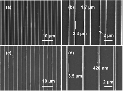 | ||
| Fig. 5 FE-SEM images of imprinted lines of TAP-0.5 (a and b) before and (c and d) after calcination. | ||
To substantiate the applicability of this thiol–ene approach for patterning other oxides, Ta2O5 was chosen as the candidate due to its potential applications in semiconducting devices.68,69 Although tantalum is a pentavalent metal, we used 4 equivalents of AAAc in order to match with the corresponding titanium precursor. The resultant resin was found to have a good shelf life of more than a month. The PETMP ratio to the AAAc was fixed in the similar fashion to that used in TAP-0.5 and the FT-IR analyses before and after UV light exposure were performed (Fig. S7†). The results revealed the disappearance of the –SH stretching peak, indicating the occurrence of thiol–ene photo-click chemistry. Fig. 6 shows the TGA, XRD and diffuse reflectance spectra of the tantalum-containing resin. The TGA profile was observed to be in similar nature to that of TAP-0.5. The complete mass loss was found to occur at ∼530 °C and the residual inorganic mass corresponding to Ta2O5 was observed to be 20.1%. The XRD pattern of Ta2O5 was found to be broad, indicating its amorphous nature at this temperature. Therefore, the UV-cured film was calcined at 700 °C to obtain crystalline Ta2O5. The XRD analysis of this sample revealed well-defined orthorhombic crystalline phase of Ta2O5 (JCPDS no. 79-1375).70 The diffuse reflectance and the corresponding Kubelka–Munk plots revealed a shallow spectrum for the 450 °C calcined sample, confirming the amorphous nature of the Ta2O5. The thin film calcined at 700 °C was found to exhibit a band gap of 4.26 eV, which is similar to that reported in the literature.71
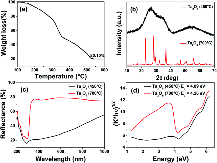 | ||
| Fig. 6 (a) Thermogravimetric analysis of tantalum-containing resin. (b) XRD patterns, (c) diffuse reflectance spectra and (d) Kubelka–Munk plots of Ta2O5 obtained at 450 and 700 °C. | ||
UV imprint lithography of the tantalum-containing resin was performed and the FE-SEM images corresponding to the as-imprinted and calcined samples are shown in Fig. 7. The line and space feature sizes of the as-imprinted patterns were found to be ∼1.7 and ∼2.1 μm, respectively. After calcination, the lines were shrunk to ∼470 nm and the spaces extended to ∼3.4 μm. The cross-sectional view of FE-SEM images of the as-imprinted and calcined samples showed the heights to be ∼1.7 μm and 410 nm, respectively. Thus, the lateral and vertical shrinkages were found to be ∼75% that is similar to the case of TiO2. The very similar imprinting behavior of tantalum-containing resin shows the capability of the thiol–ene approach to be a potential route for fabricating nanostructures of a host of oxides that could find applications in various devices.
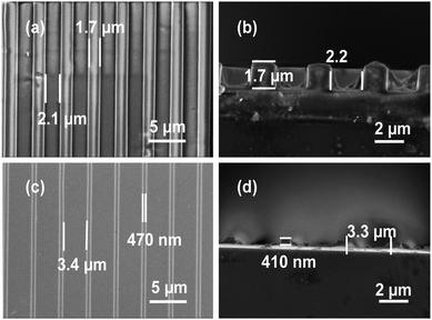 | ||
| Fig. 7 Areal (a and c) and cross-sectional (b and d) FE-SEM images of as-imprinted (a and b) and post-calcined (c and d) imprints of tantalum-containing resin. | ||
4. Conclusion
In summary, thiol–ene photo-click chemistry has been successfully applied to the fabrication of metal oxide micro/nanostructures via imprinting. When PETMP and AAAc were mixed to keep the allyl to thiol ratio as 1![[thin space (1/6-em)]](https://www.rsc.org/images/entities/char_2009.gif) :
:![[thin space (1/6-em)]](https://www.rsc.org/images/entities/char_2009.gif) 1, the FT-IR studies revealed poor efficiency of the thiol–ene photo-click chemistry. When allyl to thiol ratio was kept as 1
1, the FT-IR studies revealed poor efficiency of the thiol–ene photo-click chemistry. When allyl to thiol ratio was kept as 1![[thin space (1/6-em)]](https://www.rsc.org/images/entities/char_2009.gif) :
:![[thin space (1/6-em)]](https://www.rsc.org/images/entities/char_2009.gif) 0.5, the thiol–ene photo-click chemistry was found to be efficient under ambient conditions, possibly due to the enhanced probability of the reaction between –SH group and the abundant alkene. The metal-containing resin consisted of chelated titanium alkoxide with AAAc (or MAEAA) with suitable proportion of PETMP cross-linker, and HMP photo-initiator. With the optimal amount of allyl to thiol ratio as 1
0.5, the thiol–ene photo-click chemistry was found to be efficient under ambient conditions, possibly due to the enhanced probability of the reaction between –SH group and the abundant alkene. The metal-containing resin consisted of chelated titanium alkoxide with AAAc (or MAEAA) with suitable proportion of PETMP cross-linker, and HMP photo-initiator. With the optimal amount of allyl to thiol ratio as 1![[thin space (1/6-em)]](https://www.rsc.org/images/entities/char_2009.gif) :
:![[thin space (1/6-em)]](https://www.rsc.org/images/entities/char_2009.gif) 0.5 (TAP-0.5), the resin exhibited excellent photo-curability to yield stable, crack-free, and dry thin film. The XRD and Raman analyses revealed the formation of anatase TiO2 phase at temperatures below 550 °C, above which a small amount of rutile formation was confirmed with XRD. The diffuse reflectance spectroscopy revealed the semiconducting nature of the thin film TiO2. The imprinting studies demonstrated the patternability of the titanium-containing resin to fabricate micro/nanostructures of TiO2. Successful extension of this thiol–ene photo-click chemistry for patterning Ta2O5 confirmed the leeway of this approach towards fabrication of various functional oxide nanostructures.
0.5 (TAP-0.5), the resin exhibited excellent photo-curability to yield stable, crack-free, and dry thin film. The XRD and Raman analyses revealed the formation of anatase TiO2 phase at temperatures below 550 °C, above which a small amount of rutile formation was confirmed with XRD. The diffuse reflectance spectroscopy revealed the semiconducting nature of the thin film TiO2. The imprinting studies demonstrated the patternability of the titanium-containing resin to fabricate micro/nanostructures of TiO2. Successful extension of this thiol–ene photo-click chemistry for patterning Ta2O5 confirmed the leeway of this approach towards fabrication of various functional oxide nanostructures.
Conflicts of interest
There are no conflicts to declare.Acknowledgements
R. G. thanks the Department of Science & Technology (SERB/F/825/2014-15) for the financial aid. He also thanks Department of Science and Technology – fund for improvement of science and technology infrastructure (DST FIST; SR/FST/CSI-240/2012) to procure FT-IR, Raman microscopy, and UV-visible spectroscopy.References
- L. M. S. Ramirez, M. He, S. Mailloux, J. George and J. Wang, Small, 2016, 12, 3259–3269 CrossRef CAS PubMed.
- H. C. Kolb and K. B. Sharpless, Drug Discovery Today, 2003, 8, 1128–1137 CrossRef CAS PubMed.
- C. H. Kim, J. H. Bang, K. B. Hong and M. H. Park, RSC Adv., 2016, 6, 96700–96705 RSC.
- L. Ruizendaal, S. P. Pujari, V. Gevaerts, J. M. Paulusse and H. Zuilhof, Chem.–Asian J., 2011, 6, 2776–2786 CrossRef CAS PubMed.
- O. Z. Durham, H. R. Norton and D. A. Shipp, RSC Adv., 2015, 5, 66757–66766 RSC.
- T. Modjinou, H. Rodriguez-Tobias, G. Morales, D. L. Versace, V. Langlois, D. Grande and E. Renard, RSC Adv., 2016, 6, 88135–88142 RSC.
- Y. B. Zhou and Z. P. Zhan, Chem.–Asian J., 2018, 13, 9–19 CrossRef CAS PubMed.
- C. E. Hoyle and C. N. Bowman, Angew. Chem., Int. Ed., 2010, 49, 1540–1573 CrossRef CAS PubMed.
- A. B. Lowe, Polym. Chem., 2010, 1, 17–36 RSC.
- A. B. Lowe, Polym. Chem., 2014, 5, 4820–4870 RSC.
- M. J. Kade, D. J. Burke and C. J. Hawker, J. Polym. Sci., Part A: Polym. Chem., 2010, 48, 743–750 CrossRef CAS.
- J. Tan, C. Li, J. Zhou, C. Yin, B. Zhang, J. Gu and Q. Zhang, RSC Adv., 2014, 4, 13334–13339 RSC.
- L. M. Campos, K. L. Killops, R. Sakai, J. M. Paulusse, D. Damiron, E. Drockenmuller, B. W. Messmore and C. J. Hawker, Macromolecules, 2008, 41, 7063–7070 CrossRef CAS.
- T. R. Hayes, P. A. Lyon, E. Silva-Lopez, B. Twamley and P. D. Benny, Inorg. Chem., 2013, 52, 3259–3267 CrossRef CAS PubMed.
- L. A. Connal, C. R. Kinnane, A. N. Zelikin and F. Caruso, Chem. Mater., 2009, 21, 576–578 CrossRef CAS.
- J. Xu and C. Boyer, Macromolecules, 2015, 48, 520–529 CrossRef CAS.
- A. V. Bordoni, M. V. Lombardo and A. Wolosiuk, RSC Adv., 2016, 6, 77410–77426 RSC.
- Z. Xu, M. Yin, J. Sun, G. Ding, L. Lu, P. Chang, X. Chen and D. Li, Nanotechnology, 2016, 27, 115401–115411 CrossRef PubMed.
- J. Na, Y. Kim, C. Park and E. Kim, NPG Asia Mater., 2015, 7, 217–223 CrossRef.
- P. Hu, G. Du, W. Zhou, J. Cui, J. Lin, H. Liu, D. Liu, J. Wang and S. Chen, ACS Appl. Mater. Interfaces, 2010, 2, 3263–3269 CAS.
- S. G. Kumar and L. G. Devi, J. Phys. Chem. A, 2011, 115, 13211–13241 CrossRef CAS PubMed.
- N. Tohge, R. Ueno, F. Chiba, K. Kintaka and J. Nishii, J. Sol-Gel Sci. Technol., 2000, 19, 119–123 CrossRef CAS.
- L. Li, S. Chakrabarty, K. Spyrou, C. K. Ober and E. P. Giannelis, Chem. Mater., 2015, 27, 5027–5031 CrossRef CAS.
- M. Saifullah, K. Subramanian, E. Tapley, D.-J. Kang, M. Welland and M. Butler, Nano Lett., 2003, 3, 1587–1591 CrossRef CAS.
- D. Garoli and G. Della Giustina, Mater. Chem. Phys., 2015, 164, 63–70 CrossRef CAS.
- N. E. Voicu, M. Saifullah, K. Subramanian, M. E. Welland and U. Steiner, Soft Matter, 2007, 3, 554–557 RSC.
- S. Lee, S. H. Jung, D. J. Kang and J. Lee, RSC Adv., 2016, 6, 5944–5948 RSC.
- E. B. Duoss, M. Twardowski and J. A. Lewis, Adv. Mater., 2007, 19, 3485–3489 CrossRef CAS.
- S. Sung, S. Park, S. Cha, W. J. Lee, C. H. Kim and M. H. Yoon, RSC Adv., 2015, 5, 38125–38129 RSC.
- L. Fu, X. Liu, Y. Zhang, V. P. Dravid and C. A. Mirkin, Nano Lett., 2003, 3, 757–760 CrossRef CAS.
- M. Su, X. Liu, S.-Y. Li, V. P. Dravid and C. A. Mirkin, J. Am. Chem. Soc., 2002, 124, 1560–1561 CrossRef CAS PubMed.
- S. H. Lim, M. Saifullah, H. Hussain, W. W. Loh and H. Y. Low, Nanotechnology, 2010, 21, 285303–285308 CrossRef PubMed.
- M. Li, H. Tan, L. Chen, J. Wang and S. Y. Chou, J. Vac. Sci. Technol., B: Microelectron. Nanometer Struct.--Process., Meas., Phenom., 2003, 21, 660–663 CrossRef CAS.
- H. H. Park, D. G. Choi, X. Zhang, S. Jeon, S. J. Park, S. W. Lee, S. Kim, K. d. Kim, J. H. Choi and J. Lee, J. Mater. Chem., 2010, 20, 1921–1926 RSC.
- S. Azimi, J. Song, C. Li, S. Mathew, M. Breese and T. Venkatesan, Nanotechnology, 2014, 25, 445301–445308 CrossRef CAS PubMed.
- M. Faustini, C. Boissiere, L. Nicole and D. Grosso, Chem. Mater., 2013, 26, 709–723 CrossRef.
- E. A. Costner, M. W. Lin, W. L. Jen and C. G. Willson, Annu. Rev. Mater. Res., 2009, 39, 155–180 CrossRef CAS.
- K. J. Byeon and H. Lee, Eur. Phys. J.: Appl. Phys., 2012, 59, 10001 CrossRef.
- J. G. Ok, Y. J. Shin, H. J. Park and L. J. Guo, Appl. Phys. A, 2015, 121, 343–356 CrossRef CAS.
- D. G. Choi, K. J. Lee, S. Kim, E. S. Lee, J. H. Jeong, J. Lee and J. H. Choi, RSC Adv., 2012, 2, 11035–11039 RSC.
- D. J. Resnick, S. Sreenivasan and C. G. Willson, Mater. Today, 2005, 8, 34–42 CrossRef CAS.
- T. S. Kustandi, W. W. Loh, H. Gao and H. Y. Low, ACS Nano, 2010, 4, 2561–2568 CrossRef CAS PubMed.
- S. Takei, T. Ogawa, R. Deschner and C. G. Willson, Microelectron. Eng., 2014, 116, 44–50 CrossRef CAS.
- N. Kooy, K. Mohamed, L. T. Pin and O. S. Guan, Nanoscale Res. Lett., 2014, 9, 320–322 CrossRef PubMed.
- S. H. Ahn and L. J. Guo, ACS Nano, 2009, 3, 2304–2310 CrossRef CAS PubMed.
- R. Ganesan, J. Dumond, M. S. Saifullah, S. H. Lim, H. Hussain and H. Y. Low, ACS Nano, 2012, 6, 1494–1502 CrossRef CAS PubMed.
- O. F. Gobel, M. Nedelcu and U. Steiner, Adv. Funct. Mater., 2007, 17, 1131–1136 CrossRef.
- S. J. Kwon, J. H. Park and J. G. Park, J. Electroceram., 2006, 17, 455–459 CrossRef CAS.
- E. Zanchetta, V. Auzelyte, J. Brugger, A. V. Savegnago, G. Della Giustina and G. Brusatin, Microelectron. Eng., 2012, 98, 176–179 CrossRef CAS.
- J. H. Choi, H. B. Jo, H. J. Choi and H. Lee, Nanotechnology, 2013, 24, 195301–195308 CrossRef PubMed.
- R. Kothari, M. R. Beaulieu, N. R. Hendricks, S. Li and J. J. Watkins, Chem. Mater., 2017, 29, 3908–3918 CrossRef CAS.
- G. Rasic and J. Schwartz, MRS Commun., 2013, 3, 207–211 CrossRef CAS.
- R. Ganesan, S. H. Lim, M. Saifullah, H. Hussain, J. X. Kwok, L. Ryan, H. A. Bo and H. Y. Low, J. Mater. Chem., 2011, 21, 4484–4492 RSC.
- S. S. Dinachali, M. S. Saifullah, R. Ganesan, E. S. Thian and C. He, Adv. Funct. Mater., 2013, 23, 2201–2211 CrossRef CAS.
- S. S. Dinachali, J. Dumond, M. S. M. Saifullah, K. K. Ansah-Antwi, R. Ganesan, E. S. Thian and C. He, ACS Appl. Mater. Interfaces, 2013, 5, 13113–13123 CAS.
- R. Nagarjuna, S. Roy and R. Ganesan, Microporous Mesoporous Mater., 2015, 211, 1–8 CrossRef CAS.
- S. Challagulla, R. Nagarjuna, R. Ganesan and S. Roy, ACS Sustainable Chem. Eng., 2016, 4, 974–982 CrossRef CAS.
- E. C. Hagberg, M. Malkoch, Y. Ling, C. J. Hawker and K. R. Carter, Nano Lett., 2007, 7, 233–237 CrossRef CAS PubMed.
- L. M. Campos, I. Meinel, R. G. Guino, M. Schierhorn, N. Gupta, G. D. Stucky and C. J. Hawker, Adv. Mater., 2008, 20, 3728–3733 CrossRef CAS.
- H. Lin, X. Wan, X. Jiang, Q. Wang and J. Yin, Adv. Funct. Mater., 2011, 21, 2960–2967 CrossRef CAS.
- X. Hu, S. Huang, R. Gu, C. Yuan, H. Ge and Y. Chen, Macromol. Rapid Commun., 2014, 35, 1712–1718 CrossRef CAS PubMed.
- M. Pelaez, N. T. Nolan, S. C. Pillai, M. K. Seery, P. Falaras, A. G. Kontos, P. S. Dunlop, J. W. Hamilton, J. A. Byrne and K. O'shea, Appl. Catal., B, 2012, 125, 331–349 CrossRef CAS.
- L. Song, A. Abdelsamie, C. J. Schaffer, V. Korstgens, W. Wang, T. Wang, E. D. Indari, T. Froschl, N. Husing and T. Haeberle, Adv. Funct. Mater., 2016, 26, 7084–7093 CrossRef CAS.
- C. Pina-Hernandez, V. Lacatena, G. Calafiore, S. Dhuey, K. Kravtsov, A. Goltsov, D. Olynick, V. Yankov, S. Cabrini and C. Peroz, Nanotechnology, 2013, 24, 065301–065306 CrossRef PubMed.
- W. Su, J. Zhang, Z. Feng, T. Chen, P. Ying and C. Li, J. Phys. Chem. C, 2008, 112, 7710–7716 CAS.
- A. L. Linsebigler, G. Lu and J. T. Yates Jr, Chem. Rev., 1995, 95, 735–758 CrossRef CAS.
- S. Challagulla, K. Tarafder, R. Ganesan and S. Roy, Sci. Rep., 2017, 7, 8783 CrossRef PubMed.
- X. Lü, S. Ding, T. Lin, X. Mou, Z. Hong and F. Huang, Dalton Trans., 2012, 41, 622–627 RSC.
- D. Zhao, C. Zhang, H. Kim and L. J. Guo, Adv. Energy Mater., 2015, 5, 1500768 CrossRef.
- S. Dhawan, T. Dhawan and A. G. Vedeshwar, J. Alloys Compd., 2016, 657, 366–371 CrossRef CAS.
- W. J. Chun, A. Ishikawa, H. Fujisawa, T. Takata, J. N. Kondo, M. Hara, M. Kawai, Y. Matsumoto and K. Domen, J. Phys. Chem. B, 2003, 107, 1798–1803 CrossRef CAS.
Footnote |
| † Electronic supplementary information (ESI) available. See DOI: 10.1039/c8ra01688g |
| This journal is © The Royal Society of Chemistry 2018 |

