 Open Access Article
Creative Commons Attribution 3.0 Unported Licence
Comprehensive studies of temperature and frequency dependent dielectric and a.c. conducting parameters in third generation multi-component glasses
Namrata Chandelab,
M. M. A. Imranc and
Neeraj Mehta *a
*a
aGlass Science Laboratory, Department of Physics, Banaras Hindu University, Varanasi-221005, India. E-mail: dr_neeraj_mehta@yahoo.co.in
bDepartment of Physics, Sunbeam College for Women, Varanasi-221005, India
cDepartment of Physics, Faculty of Science, Al-Balqa Applied University, Al-Salt 19117, Jordan
First published on 16th July 2018
Abstract
The dielectric relaxation and thermally assisted a.c. conduction play an important role in understanding the conduction mechanism in chalcogenide glasses. These two phenomena are often the deciding factors of the suitability of chalcogenide materials for particular device applications. Dielectric relaxation studies are important to understand the nature and origin of dielectric losses, which, in effect, may be useful in the determination of structure and defects in solids. The study of thermally assisted a.c. conduction can be used as a tool to understand the nature of defect states and the estimation of their density of defect states. In this paper, therefore, we have studied the metal-induced effects of cadmium (Cd), indium (In) and antimony (Sb) on dielectric relaxation and thermally activated a.c. conduction in ternary Se80Te18Sn2 glass. The density of charged defect states in quaternary Se80Te8Sn2M10 alloys is found to vary with the electro-negativity difference (ξM − ξTe) of the foreign element M and Te. Further analysis shows that the increasing sequence of the density of charged defects is explained in terms of variation in the lone-pair electrons after the incorporation of Cd, In and Sb.
1. Introduction
Glasses are distinct from ordinary non-crystalline materials. Unlike usual non-crystalline materials, they possess a glass transition.1 In the family of glasses, the semiconducting chalcogenide crystals and glasses have drawn considerable interest in areas of solid-state physics, chemistry and materials science because of their exciting commercial applications and properties.2–6 Recently, chalcogen rich non-oxide glasses have found use in potential applications in phase-change data storage,2 electronic tongues,3 and memory cells.4These materials have recently come under scientific scrutiny due to the strong relation between their electronic properties and disordered structure.7 A relevant and complete understanding of their electrical transport properties is, therefore, an area of on-going research activity.8,9 The basic goal behind such studies is to explore the electrical properties of chalcogenide glasses for further practical utilization. A common characteristic of semiconducting chalcogenide glasses is the presence of localized states in the mobility gap due to the lack of long-range order (LRO) and intrinsic defects. The conductivity in crystalline chalcogenides10 and chalcogenide glasses11 is usually suggested to be p-type. The idea of p-type conduction is based on the asymmetry of the conduction band (formed of anti-bonding orbitals) and the valence band (constituted by non-bonding or lone-pair electrons). It was suggested that the degree of the disorder should have more consequence on anti-bonding states as compared to non-bonding states.12 Therefore, the range of localized tail states at the valence band edge is less in comparison to the localized states at the conduction band edge. As a consequence, the number of electrons excited over the conduction band mobility edge is less than the number of holes excited below the valence band mobility edge. This is probably one of the reasons that chalcogenide glasses show p-type conductivity. Thus, the knowledge of the transport mechanism and estimation of the density of charged defect states is a significant study to understand the complete picture of electric conduction in chalcogen rich materials.
Dielectric and a.c. conduction properties of PVC gels, polymers, organic semiconductors and semiconducting glasses are considered as a significant tool for better understanding of the transport mechanism8,13–15 and novel phenomenon9 in such materials. Mott, Elliott and Davis proposed several band models in a series of papers for the explanation of the dielectric behavior and electronic structure of non-crystalline soft materials.16 Dielectric relaxation studies are important to understand the nature and the origin of loss, which in turn may be useful in the determination of the structure and defects in such solids.17,18 The dielectric dispersion is not expected in pure glassy selenium at low frequencies,19,20 as these materials are covalently bonded solids. However, the past measurements done by our and other groups21,22 indicate that the dielectric dispersion does exist in these glasses even at low frequencies. The origin and the nature of dielectric losses in these materials has, therefore, become a matter of curiosity. Investigations of the frequency and temperature dependence of the a.c. conductivity of chalcogenide glasses are also proved significant tools for understanding the nature of conduction mechanism in these materials.17,18 Therefore, we have synthesized novel third-generation multi-component glasses of SeTeSnM (where M is metallic impurity) by incorporating Cd, In and Sb as chemical modifier M in second generation SeTeSn glass. Further, we have studied the dependence of dielectric constant, loss, a.c. conductivity and the related parameters on temperature/frequency. These new studies are directly important to understand the “metallic-induced consequence” of dielectric relaxation and thermally assisted a.c. conduction. In past five decades, lots of work is done for establishing the glass forming regions on binary and ternary glasses, but no sufficient literature is available for quaternary glasses. Thus, we have started to incorporate such elements in Se–Te–Sn system; that show excellent glass forming tendency (GFT) and high thermal stability (TS) with Se–Te–Sn system so that it may be used as potential candidate for the optical memory applications.2
Efforts have been made by various workers frequently to investigate the compositional effects of a particular foreign element on dielectric and a.c. conducting parameters of all the three generations of these materials.17–22 To the best of our knowledge, no serious attempts have been done to make inquiries: what happens if we replace the doping element at fixed composition instead of inverse but the usual trend. Thus, this report of third generation glasses, where the composition is fixed and modifications have been analyzed by alteration of foreign atoms.
2. Experimental
2.1 Synthesis route
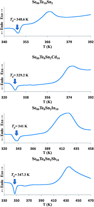
The exact proportions of high purity (99.999%) elements (purchased from Alfa Aesar), in accordance with their atomic percentages, were weighed using an electronic balance with the least count of 10−4 g. The materials were then sealed in evacuated (∼10−6 torr) quartz ampoules having length ∼5 cm and internal diameter ∼8 mm. The ampoules containing the constituent elements were heated to an appropriate temperature (∼650 °C) in a muffle furnace whose temperature was raised slowly at a rate of 3–4 °C per minute.The thermal characterization was investigated using a differential scanning calorimeter (T.A. Instruments, USA; Model: Auto Q20) under almost identical conditions by using same heating rate (10 K min−1) and nitrogen as purge gas. Tzero aluminum pans and lids were used to seal the samples in powder form in DSC cell. The accuracy of the heat flow in DSC was ±0.01 mW and the temperature precision as determined by the microprocessor of the thermal analyzer was ±0.1 K. Fig. 1 shows the Differential Scanning Calorimetric (DSC) scans of all samples for confirmation of the glassy nature through the occurrence of sharp endothermic peaks in glass transition region before the appearance of exothermic peaks in crystallization region.
2.2 Dielectric and a.c. conductivity measurements
Electrical measurements were investigated in the audio frequency range (0.5 kHz–1 MHz) and temperature range 300–345 K for observing the appreciable and significant dielectric relaxation and a.c. conduction mechanism. The complex dielectric function of a material is represented by two parts. Its real part is known as dielectric constant (ε′) while its imaginary part is called dielectric loss (ε′′). The experimental values of capacitance and dissipation factor measured from LCR meter were used to evaluate ε′ and ε′′.In chalcogenide glasses, the temperature/frequency dependence of dielectric constant (ε′) and dielectric loss (ε′′) are precise in the temperature range near glass transition.17–22 At temperatures lower than room temperature, ε′ is nearly constant and ε′′ is negligibly small. Above room temperature, ε′ and ε′′ are increased appreciably with temperature. Therefore, the present measurements have been made in the temperature region below the onset of glass transition region where dielectric dispersion is quite appreciable.
For measurements of dielectric constant and dielectric loss, all the glassy alloys were ground to a very fine powder and pellets (diameter ∼ 10 mm and thickness ∼ 1 mm) were obtained by compressing the powder in a die at a load of 5 tons. The pellets were coated with indium film to ensure good electrical contact between the sample and the electrodes. A specially designed metallic sample holder has been used for dielectric measurements. The temperature measurement was facilitated by a copper-constantan thermocouple mounted very near to the sample. An O-ring was present between the two parts of the sample holder for suitable evacuation inside the chamber. A vacuum of ∼10−3 torr was maintained over the entire temperature range from room temperature to near the glass transition region. Dielectric measurements were made using a digital LCR meter (Wayne Kerr Electronics, Model: 4100).
For accurate measurements and convenience, the sample is taken in cylindrical geometry. This can be achieved by pressing the powdered sample to prepare pellets since as-prepared materials cannot be shaped directly in perfect cylindrical geometry due to brittleness. Also, we preferred to experiment on the pellet rather than the bulk as macroscopic effects (gas bubbles, etc.) may appear in the bulk during preparation. It is already observed (both theoretically and experimentally) by Goyal et al.19 that bulk ingots and compressed pellets exhibit similar dielectric behavior in chalcogenide glasses.
3. Theoretical formalism to determine electrical parameters
Knowing the experimental values of the parallel capacitance and dissipation factor, the dielectric constant ε′ and dielectric values ε′′ can be calculated by using following relations:| ε′ = C/C0 | (1) |
| ε′′ = ε′D | (2) |
According to the model proposed by Guintini et al.,23 the dielectric loss (ε′′) at a particular frequency, in the temperature range where dielectric dispersion occurs, is expressed by the following relation:
| ε2 = (εs − ε∞)2π2N(ne2/εs)3kBTτm0Wm−4ωm | (3) |
Here m is the power of angular frequency (ω) and it is given by:
 | (4) |
The value of a.c. conductivity is calculated by the relation:
| σac(ω) = ωε′′ε0 | (5) |
4. Results and discussion
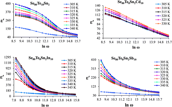
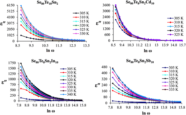
The frequency dependence of dielectric constant for the present glassy SeTeSnM system at different temperatures is shown in Fig. 2. A strong frequency dispersion of ε′ is observed in the low-frequency region followed by almost frequency independent behavior beyond ∼10 kHz for all temperatures. It is revealed from these plots that the values of ε′ increase with increase in temperature at all frequencies for the present glassy system. This increment is found different for different frequencies. The observed large values of ε′ in the lower frequency range can be explained on the basis of the Maxwell–Wagner model.24 According to Koops's theory,25 the solid is assumed to be formed of well-conducting grains separated by highly resistive thin layers and grain boundaries. As a result of the applied signal to the material, a space charge polarization is built up at the grain boundaries. The induced space charge polarization is restricted by the available free charges on the grain boundary and the conductivity of the sample. Further, Koops's model suggests that the major contribution of the dielectric constant at low frequency comes from the grain boundaries, which have a high dielectric constant. On the other hand, at high frequency, the dielectric behavior of the material is dominated by the grains which have a small dielectric constant. The decrease of ε′ with the increase in frequency may be recognized by the electrical relaxation processes.The frequency dependence of the imaginary component of the dielectric function, i.e., dielectric loss ε′′ for the present glassy system in the aforesaid frequency and temperature region is represented in Fig. 3. It is obvious from these plots that the dielectric loss also has large values in the low-frequency range that are decreased with increasing frequency. At higher frequencies, ε′′ has no remarkable changes at all temperatures. In the low-frequency region, which corresponds to high resistivity due to the main cause of the grain boundaries at lower frequencies, more energy is required for hopping between the levels. Therefore the energy loss is high at lower frequencies. In the high-frequency region, the less energy is required for electron movement between the levels and thus the energy loss is small. The inverse frequency dependence of the dielectric loss at low frequencies was evidence of the non-Debye type character of the overall relaxation. It is well known that in Debye-type relaxation, the loss factor should increase with increasing frequency.
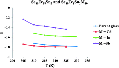
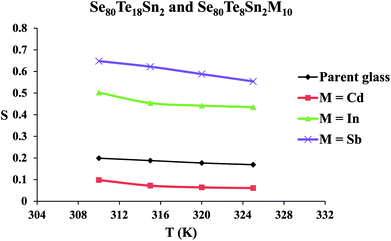
The frequency exponent (m) is obtained by least squares fitting of the experimental data and is plotted as a function of temperature in Fig. 4 for multi-component glasses. It is clear from these plots that the calculated values of the frequency exponent m are decreased with increasing temperature. This observation is consistent with Guintini23 theory which shows that the dielectric relaxation is related to the hopping of charge carriers over a potential barrier.
The temperature dependency of ε′ at various frequencies is represented in Fig. 5 for the present glassy system. These plots clearly indicate that ε′ increases with the increase in temperature at all frequencies. Further, it is also evident from these figures that ε′ shows strong temperature dependence in the low-frequency region. On the other hand, it exhibits weak temperature dependence in the high-frequency region. Such temperature dependence of ε′ can be explained in terms of orientational polarization which is associated with the thermal motion of molecules. At relatively low temperatures, the dipoles cannot orient themselves with respect to the track of the applied field. Consequently, their contribution to the polarization and the dielectric constant is weak. As the temperature rises, the bound charge carriers get sufficient excitation thermal energy and they become capable to follow the change in the external field more easily. This, in turn, enhances their involvement with the polarization leading to an increase in the dielectric constant of the sample.26
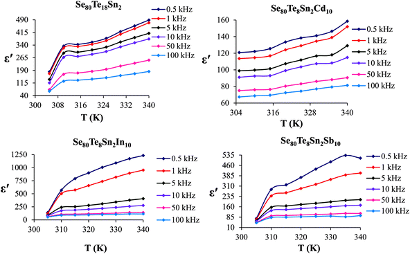 | ||
| Fig. 5 Temperature dependence of dielectric constant for glassy Se80Sn2Te18 and Se80Te8Sn2M10 alloys. | ||
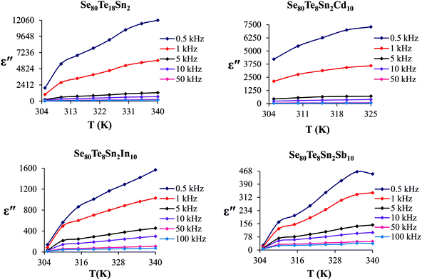
Fig. 6 shows the temperature dependence of ε′′ at various frequencies. It is obvious from these figures that ε′′ also increases with increasing temperature. Unlike the electronic and ionic polarization, the orientational polarization involves associative motions of molecular segments in a viscous medium and it depends on temperature. It is well known that the rise in temperature leads to a fall in viscosity of the medium. The effect of the drop in viscosity on the amount of the dielectric loss can be considered as an increase in the internal friction of matter when the dipole rotates through a unit angle. Interfacial or space charge polarization is an additional feature that should be recognized and accounted for the explanation of experimental outcomes. This type of polarization is due to the migration of electrons or ions over distances of macroscopic scale. Distinct from deformational polarization (electronic and ionic), the relaxation polarization (orientational and interfacial) needs a quite long time and dissipates electric energy that transforms into heat in a dielectric, i.e., this energy causes dielectric loss. According to Stevels,26 the relaxation phenomenon divided in following three parts: (i) conduction loss, (ii) dipole loss and (iii) vibrational loss. The conduction loss has a minimum value at the low temperature because it is proportional to σac(f)/f. Since σac(f) increases with increasing temperature, therefore it causes the increase in conduction losses. Consequently, the value of ε′′ is increased with increase in temperature. The other two losses involve the migration of ions over large distances. This motion is the same as that occurring under direct current conditions. The ions jump over the highest barriers in the network. At low-temperature values, conduction, dipole and vibration losses have the minimum value. However at higher temperatures, as the temperature increases, the hopping process increases and since the conduction is due to hopping from one localized states to the another, thus the conduction increases and so the losses due to conduction also increases. Additionally, dipole and vibration losses also increase.
Structural studies of chalcogenide glasses are very important for better understanding of transport mechanisms. A.c. conductivity measurements have been widely used to investigate the nature of defect centers in disordered systems since it is assumed that they are responsible for this type of conduction. The general frequency behavior in this type of materials is of Aωs type over a wide frequency range where exponent s is found to be temperature dependent and has a value ≤ 1. Various models have been formulated to explain this behavior and classical approach is to consider a.c. and d.c. conduction separately.
The a.c. conductivity in semiconductors has been interpreted in terms of the pair approximation. In this approximation, a pair consists of two localized states between which electronic carriers move back and forth with a particular relaxation time. In amorphous semiconductors, the localized states have been considered to be randomly distributed in the space, and pairs with various relaxation times exist. The a.c. conductivity is the sum of contributions from all the pairs.
A.c. conductivity σac(ω) can be modeled by a power law:27
| σac(ω) = σtot(ω) − σdc(ω) = Aωs | (6) |
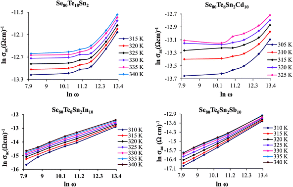 | ||
Fig. 7 Plots of ln![[thin space (1/6-em)]](https://www.rsc.org/images/entities/char_2009.gif) σac vs. ln σac vs. ln![[thin space (1/6-em)]](https://www.rsc.org/images/entities/char_2009.gif) ω for glassy Se80Te18Sn2 and Se80Te8Sn2M10 alloys at different temperatures. ω for glassy Se80Te18Sn2 and Se80Te8Sn2M10 alloys at different temperatures. | ||
The plots of σac against 1000/T for all glasses at different frequencies are shown in Fig. 9 for the glassy SeTeSnM system. From these plots, one can see that σac increases with increase in frequency. It is also clear from these figures that σac increases linearly with decreasing the reciprocal of absolute temperature. This clearly indicates that σac has Arrhenian temperature dependence. Arrhenian temperature dependence is generally observed in a variety of physical and chemical quantities during studies of different kinds.28–32
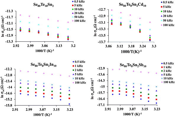 | ||
Fig. 9 Plots of ln![[thin space (1/6-em)]](https://www.rsc.org/images/entities/char_2009.gif) σac against 1000/T at different frequencies for glassy Se80Te18Sn2 and Se80Te8Sn2M10 alloys. σac against 1000/T at different frequencies for glassy Se80Te18Sn2 and Se80Te8Sn2M10 alloys. | ||
In other words, the a.c. conduction is a thermally activated process due to hopping in the localized states between the gap or band tails. From these plots, it is clear that the variation of a.c. conductivity with temperature can approximately be expressed by well known Arrhenius relation in the intermediate temperature range as:16,33
 | (7) |
| Frequency (kHz) | Eac (eV) | |||
|---|---|---|---|---|
| Se80Te18Sn2 | Se80Te8Sn2Cd10 | Se80Te8Sn2In10 | Se80Te8Sn2Sb10 | |
| 0.5 | 0.25 | 0.23 | 0.31 | 0.33 |
| 10 | 0.22 | 0.21 | 0.24 | 0.20 |
| 20 | 0.20 | 0.20 | 0.22 | 0.17 |
| 100 | 0.18 | 0.16 | 0.16 | 0.14 |
Like other functional materials,34–36 chalcogenide glasses also follow correlated barrier hopping model and therefore the advantages of a.c. measurements are that they permit investigations of time-dependent properties such as polaron hopping and information of other processes occurring in the material. Such measurement also helps to estimate the density of charged defect states.37
As mentioned earlier, the a.c. conduction in chalcogenide glasses can be explained in terms of both single polaron hopping and bi-polaron hopping. With this point of view, the experimental data have been fitted according to CBH model. The fitting has been applied to the product NNp of N and Np for achieving a satisfactory agreement between the theoretical and experimental curves of ln![[thin space (1/6-em)]](https://www.rsc.org/images/entities/char_2009.gif) σac(ω) versus 1000/T. The fitting has been done at a frequency of 10 kHz. The values of Wm for different alloys are calculated using temperature dependence of exponent s:27
σac(ω) versus 1000/T. The fitting has been done at a frequency of 10 kHz. The values of Wm for different alloys are calculated using temperature dependence of exponent s:27
 | (8) |
Fig. 10 shows the contributions of single-polaron and bi-polaron hopping and their sum to the thermally assisted a.c. conduction at a frequency of 10 kHz. In these plots, the points shown by symbols  ,
,  ,
,  and
and  stand for experimental a.c. conductivity (σac)exp, the contribution of single polaron hopping to a.c. conductivity (σac)si, contribution of bi-polaron hopping to a.c. conductivity (σac)bi and theoretical a.c. conductivity (σac)theor respectively. As seen from these figures, theoretical curves are in good agreement with the experimental results. It is also clear from these figures that bi-polaron contribution is dominant over single polaron for present alloys. The density of charged defect states N is evaluated from the values of NNp (where Np = N/2). The values of N are given in Table 2.
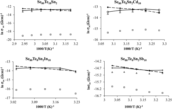 | ||
| Fig. 10 Fitting of theoretical and experimental results of a.c. conductivity for glassy Se80Te18Sn2 and Se80Te8Sn2M10 alloys. | ||
| Sample | N (cm)−3 | LP |
|---|---|---|
| Se80Te18Sn2 | 4.0 × 10²² | 3.92 |
| Se80Te8Sn2Cd10 | 7.9 × 10²⁰ | 3.32 |
| Se80Te8Sn2In10 | 1.3 × 10²² | 3.52 |
| Se80Te8Sn2Sb10 | 1.6 × 10²² | 3.67 |
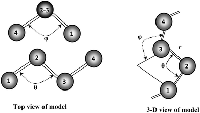
Our recent structural and Raman spectroscopic investigations of Se and Se-rich AsxSe1−x amorphous thin films suggest that all the atoms are in a twofold coordinated chain structure and not random. This so-called “random chain model” defines the angle between two adjacent bonding planes as a dihedral angle φ (see Fig. 11). The magnitude of φ remains constant with random variation in sign.38 The breakup of the Se8 ring structure takes place due to the incorporation of Te in Se–Te glasses. Consequently, the chain fraction slightly increases with some reduction in the chain length. Further incorporation of foreign elements in glass matrix of Se–Te also affects its molecular structure38 by the formation of cross-linking structures.
Keeping in mind the above model, the increase in the value of the density of localized states after incorporating the metallic additives M in parent Se80Te18Sn2 alloy can be explained to some extent in terms of average electro-negativity χ of quaternary Se80Te8Sn2M10 alloys. In the present case, we have added Cd, In and Sb in parent alloys at cost of Te. Defect states are assumed to be created because of the difference between electro-negativity ξM of the metallic additive M and that of the replaced element (here ξTe for Te) of parent alloy. It is, therefore, reasonable to expect that the difference of the density of defect states will be more where the electro-negativity difference (ξM ~ ξTe) for the quaternary alloy is large. Since defect states are assumed to be created because of the formation of alloys from constituent atoms. The values of χ for replaced element Te and incorporated atoms M are given in Table 3.39 From this table, it is clear that increasing sequence (Δξ)M=Sb < (Δξ)M=In < (Δξ)M=Cd of Δξ (=ξM − ξTe) is same as the increasing sequence of the difference of the density of charged defect states N between the parent ternary alloy and the quaternary alloys.
| Element | χ |
|---|---|
| Te | 2.618 |
| Cd | 1.978 |
| In | 2.138 |
| Sb | 2.458 |
The comparison of the effect of the fourth component (Cd, In or Sb) on the dielectric properties and a.c. conductivity is shown in Fig. 12 in terms of plots at room temperature (305 K) at two different frequencies. From these plots, one can see the significant variation in dielectric constant, loss and a.c. conductivity of parent ternary Se80Te18Sn2 glass after incorporation of Cd, In or Sb. Similar results have been observed at other temperatures and frequencies (not shown here). However, the variation in different properties for different additives is not systematic and it is highly diverse in nature.
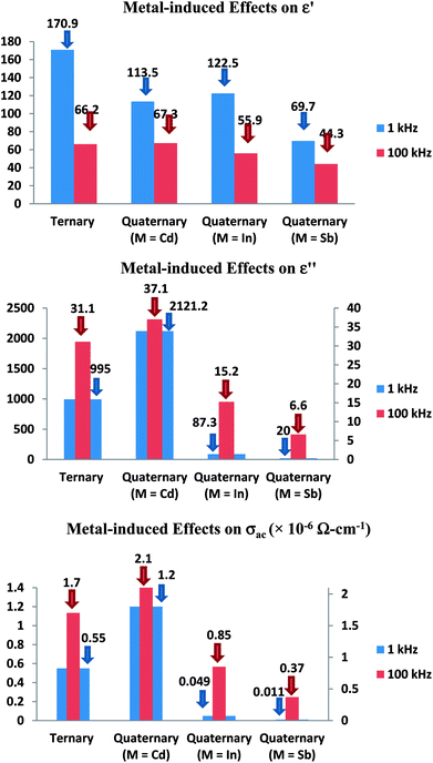 | ||
| Fig. 12 Comparison of metal-induced effects in dielectric constant, loss and a.c. conductivity of parent glass. | ||
The structure of glassy Se and the outcome of alloying Te into glassy Se have been observed by different research groups.40–43 They found the presence of long polymeric chains and rings of Se atoms in glassy Se, which are dissociated by the addition of Te in glassy Se. The successive incorporations of Sn in Se–Te glass matrix and then Cd, In and Sb in Se–Te–Sn glass matrix causes the cross-linking of Sn and Cd, In and Sb in long polymeric Se chains and Se–Te mixed chains. Thus, the dielectric constant, loss and a.c. conductivity in parent glass are changed appreciably after the addition of the fourth element. Further, the occurrence of a.c. conduction takes place from different localized states created in the gap or its tails of present selenium-rich glass due to addition of Te, Sn and Cd. Thus, the dielectric constant, loss and a.c. conductivity changes noticeably in quaternary Se80Te8Sn2M10 (M = Cd, In and Sb) glasses due to variation in the number of dangling bonds in the glassy network of the parent ternary Se80Te18Sn2 alloy.
These structural defects are not steady in the natural state. Such defects become moderately stable when polarized to positively charged and negatively charged defect states. The density of these native charged defects can be deduced from the mass action law as follows using the notation of Kastner et al.44,45
| 2C02 → C3+ + C1− | (9) |
The charged states were represented by this group as C1− and C3+. Here, the symbol C is labeled as chalcogenide and subscript indicates the atomic coordination and C02 stands for neutral center keeping in mind that an extra electron placed on C+3 is shared equally between the three bonds of the atom, which therefore remains three-fold coordinated.
In the case of pure Se, structural defects, such as dangling atoms occur because of its non-crystalline character. These structural defects are not stable in the natural state. They are fairly stable when polarized to positively charged and negatively charged defect states.
When we use the mass action law in eqn (9), we see that:
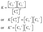 | (10) |
The neutral condition is
| [C3+] = [C1−] | (11) |
These structural defects are believed to form localized energy levels in the band gap of Se and to act is deep traps for carrier transport.
In ternary Se80Te18Sn2 alloy, all Sn atoms are probably mixed in Se atomic chains due to lower concentration, but some of Te atoms would act as ionized impurities due to the higher concentration since the electron affinity of Te is lower than that of Se.
In case of quaternary alloys i.e., the ternary alloy having incorporation of foreign additives M, some Te atoms act as positively charged impurities and metallic atoms also act as positively charged impurities. Therefore, the above neutral condition represented by eqn (11) takes the form:
| [C3+] + [Te+] + [M+] = [C1−] | (12) |
When we insert eqn (12) into (10), we obtain:
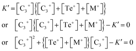 | (13) |
This is a quadratic equation in [C3+], whose solution is:
 | (14) |
Now eliminating [C3+] from eqn (12) and (10), we have:
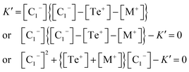 | (15) |
This is a quadratic equation in [C1−], whose solution is:
 | (16) |
From eqn (14) and (16), it is can be seen that after incorporating the metallic impurities M (M = Cd, In and Sb) into parent Se80Te18Sn2 glass, the density of structural defects is changed.
Chalcogenide glasses are frequently known as lone pair semiconductors.46,47 Lone pair electrons represent the pairs of valence electrons that do not participate in forming covalent bonds with the neighbouring atoms. The density of defect states in the band tails related to the dielectric behavior and conduction of chalcogenide glasses mark their strong dependency on lone pair electrons and.46,47 The lone pair orbits have higher energy than the bonding states and hence occupy the top of the valence band. Interactions between lone pair electrons with their local environment and different atoms result in localized states in the band tails.44
The formula for the determination of lone-pair electrons (LP) is:
| LP = V − 〈r〉 | (17) |
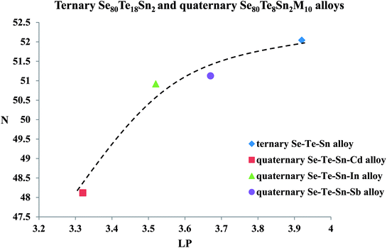 | ||
| Fig. 13 Variation of density of charged defect states N with number of lone-pair electrons LP (line is guided to eyes). | ||
Recently, we have observed that when the additives Cd, In and Sb are incorporated in the present ternary parent glass, they affects its equilibrium liquid-specific heat and glass specific heat noticeably. Thus, the present results of metal-induced effects of Cd, In and Sb on electrical properties are in consistent with that have been observed in the thermodynamic properties.48
5. Conclusions
The dielectric constant and loss both are decreased in low-frequency range, while there is no remarkable change in both parameters in higher-frequency range for all the studied glassy alloys. Both dielectric constant and loss and a.c. conductivity are changed significantly after incorporation of cadmium, indium and antimony in ternary Se80Te18Sn2 parent glass. Due to the enhancement of complexity of structure for the glassy Se–Te–Sn–M system (having four elemental components), the explanation of such anomalous behavior is not possible at this stage. The frequency dependence of a.c. conductivity obeys the power law. Further, the a.c. conductivity σac shows Arrhenius temperature dependence. The temperature dependence of frequency exponent s and its lower values (<1) verifies the applicability of the CBH model in present alloys.The results regarding the metal-induced effects of Cd, In and Sb on dielectric properties are explained in terms of the significant variation in the number of dangling bonds as suggested by Kasner's model. The effect of incorporation of Cd, In and Sb on the density of charged defect states in quaternary Se80Te8Sn2M10 alloys is explained in terms of electro-negativity difference (ξM − ξTe) and the number of lone-pair electrons. As we know that the dielectric relaxation and thermally assisted a.c. conduction play a key role for deciding the usefulness of chalcogenide glasses in various applications like dielectric mirrors, capacitive applications etc., so present results (observed as the metallic-induced consequences of both phenomena) are significant attempt to open a route for tailoring the related properties by changing chemical modifiers instead of composition.
Conflicts of interest
There are no conflicts to declare.Acknowledgements
NM is thankful to the Department of Science and Technology (DST), New Delhi, India for providing financial assistance under Fast Track Young Scientists Scheme [Scheme No. SR/FTP/PS-054/2010].References
- A. Ikeda, L. Berthier and P. Sollich, Soft Matter, 2013, 9, 7669–7683 RSC.
- D. Lencer, M. Salinga, B. Grabowski, T. Hickel, J. Neugebauer and M. Wuttig, Nat. Mater., 2008, 7, 972–977 CrossRef PubMed.
- L. M. Codinachs, J. P. Kloock, M. J. Schoning, A. Baldi, A. Ipatov, A. y. Bratov and C. J. Jorquera, Analyst, 2008, 133, 1440–1448 RSC.
- C. Schindler, I. Valov and R. Waser, Phys. Chem. Chem. Phys., 2009, 11, 5974–5979 RSC.
- D. Aldakov, A. Lefrançois and P. Reiss, J. Mater. Chem. C, 2013, 1, 3756–3776 RSC.
- M. Deschamps, C. Genevois, S. Cui, C. Roiland, L. LePolles, E. Furet, D. Massiot and B. Bureau, J. Phys. Chem. C, 2015, 119, 11852–11857 CrossRef.
- J. B. Vaney, G. Delaizir, E. Alleno, O. Rouleau, A. Piarristeguy, J. Monnier, C. Godart, M. Ribes, R. Escalier, A. Pradel, A. P. Gonçalves, E. B. Lopes, G. J. Cuello, P. Ziolkowski, E. Muller, C. Candolfi, A. Dauschera and B. Lenoira, J. Mater. Chem. A, 2013, 1, 8190–8200 RSC.
- A. Sharma and N. Mehta, RSC Adv., 2017, 7, 19085–19097 RSC.
- A. Kumar and N. Mehta, J. Mater. Chem. C, 2018, 6, 2747–2759 RSC.
- M. Ibanez, R. Hasler, Y. Liu, O. Dobrozhan, O. Nazarenko, D. Cadavid, A. Cabot and M. V. Kovalenko, Chem. Mater., 2017, 29, 7093–7097 CrossRef PubMed.
- M. A. Hughes, R. M. Gwilliam, K. Homewood, B. Gholipour, D. W. Hewak, T.-H. Lee, S. R. Elliott, T. Suzuki, Y. Ohishi, T. Kohoutek and R. J. Curry, Opt. Express, 2013, 21, 8101–8115 CrossRef PubMed.
- A. V. Kolobov, J. Non-Cryst. Solids, 1996, 198–200, 728–731 CrossRef.
- M. Ali and T. Hirai, Soft Matter, 2012, 8, 3694–3699 RSC.
- A. Alegria and J. Colmenro, Soft Matter, 2016, 12, 7709–7725 RSC.
- A. Armin, D. M. Stoltzfus, J. E. Donaghey, A. J. Clulow, R. C. R. Nagiri, P. L. Burn, I. R. Gentle and P. Meredith, J. Mater. Chem. C, 2017, 5, 3736–3747 RSC.
- N. F. Mott, Conduction in Non-Crystalline Materials, Clarendon Press, Oxford, 2nd edn, 1993 Search PubMed.
- A. S. Hassanien, J. Alloys Compd., 2016, 671, 566–578 CrossRef.
- S. S. Fouad and H. E. Atyia, J. Alloys Compd., 2016, 688, 1206–1213 CrossRef.
- D. R. Goyal, S. Walker and K. K. Srivastava, Phys. Status Solidi A, 1981, 64, 35–357 CrossRef.
- N. Choudhary and A. Kumar, Turk. J. Phys., 2005, 29, 119–125 Search PubMed.
- J. Sharma and S. Kumar, J. Alloys Compd., 2010, 506, 710–714 CrossRef.
- A. Sharma and N. Mehta, Eur. Phys. J.: Appl. Phys., 2012, 59, 10101 CrossRef.
- J. C. Guintini, J. V. Zanchetta, D. Jullen, R. Eholle and P. Hoenou, J. Non-Cryst. Solids, 1981, 45, 57–62 CrossRef.
- T. I. Koba, T. Wagner, P. J. S. Ewen and A. E. Owen, Philos. Mag. B, 1995, 71, 311–318 CrossRef.
- C. G. Koops, On the dispersion of resistivity and dielectric constant of some semiconductors at audio frequencies, Phys. Rev., 1951, 83, 121–124 CrossRef.
- J. M. Stevels, The Electrical Property of Glasses, in Hnadbuch der Physik, ed. S. W. Flugge, Springer, Berlin, 1997, vol. 20, p. 350 Search PubMed.
- S. R. Elliot, Adv. Phys., 1987, 36, 135–218 CrossRef.
- W. Linert and A. Yelon, Isokinetic relationships, Monatsh. Chem., 2013, 144, 1–2 CrossRef.
- K. M. Diederichsen, H. G. Buss and B. D. McCloskey, Macromolecules, 2017, 50, 3831–3840 CrossRef.
- S. Breuer and M. Wilkening, Dalton Trans., 2018, 47, 4105–4117 RSC.
- M. Li, J. Wang, B. Fu and Q. Hou, AIP Adv., 2015, 5, 127131 CrossRef.
- N. Mehta and A. Kumar, J. Phys. Chem. B, 2016, 120, 1175–1182 CrossRef PubMed.
- S. R. Elliott, Physics of Amorphous Materials, Longman Scientific & Technical, Essex, 2nd edn, 1990 Search PubMed.
- Y. B. Taher, N. Moutia, A. Oueslati and M. Gargouri, RSC Adv., 2016, 6, 39750–39757 RSC.
- A. Kahouli, A. Sylvestre, F. Jomni, B. Yangui and J. Legrand, J. Phys. Chem. A, 2012, 116, 1051–1058 CrossRef PubMed.
- A. Kachroudi, A. Kahouli, J. Legrand and F. Jomni, J. Phys. Chem. A, 2015, 119, 6428–6435 CrossRef PubMed.
- A. Sharma, A. Kumar and N. Mehta, Measurement, 2015, 75, 69–75 CrossRef.
- V. I. Mikla, J. M. Turovci, V. V. Mikla and N. Mehta, Prog. Solid State Chem., 2018, 49, 1–15 CrossRef.
- R. T. Sanderson, J. Am. Chem. Soc., 1983, 105, 2259–2261 CrossRef.
- G. Lucovsky, A. Mooradian, W. Taylor, G. B. Wright and R. C. Keezer, Solid State Commun., 1967, 5, 113–117 CrossRef.
- G. Lucovsky, Mater. Res. Bull., 1969, 4, 505–514 CrossRef.
- G. C. Das, M. B. Bever and D. R. Uhlmann, J. Non-Cryst. Solids, 1972, 7, 251–270 CrossRef.
- M. K. El-Mously and M. M. El-Zaidia, J. Non-Cryst. Solids, 1978, 27, 265–271 CrossRef.
- M. Kastner, D. Adlert and H. Fritzsche, Phys. Rev. Lett., 1976, 37, 1504–1507 CrossRef.
- M. Kasner, G. A. Thomas and S. R. Ovshinsky, Disordered semiconductors, Plenum Press, The University of California, 1987 Search PubMed.
- S. R. Elliott, C. N. R. Rao and J. M. Thomas, Angew. Chem., Int. Ed., 1986, 25, 31–46 CrossRef.
- R. M. Mehra, A. Ganjoo and P. C. Mathur, J. Appl. Phys., 1994, 75, 7334–7339 CrossRef.
- N. Chandel and N. Mehta, J. Phys. Chem. Solids, 2018, 115, 113–118 CrossRef.
| This journal is © The Royal Society of Chemistry 2018 |

