
 Open Access Article
 This Open Access Article is licensed under a Creative Commons Attribution-Non Commercial 3.0 Unported Licence
Inversion domain boundaries in MoSe2 layers†
Quang Duc Truong‡
 *a,
Nguyen Tuan Hung‡b,
Yuta Nakayasua,
Keiichiro Nayukic,
Yoshikazu Sasakic,
Devaraju Murukanahally Kempaiaha,
Li-Chang Yind,
Takaaki Tomaia,
Riichiro Saitob and
Itaru Honma*a
*a,
Nguyen Tuan Hung‡b,
Yuta Nakayasua,
Keiichiro Nayukic,
Yoshikazu Sasakic,
Devaraju Murukanahally Kempaiaha,
Li-Chang Yind,
Takaaki Tomaia,
Riichiro Saitob and
Itaru Honma*a
aInstitute of Multidisciplinary Research for Advanced Materials, Tohoku University, Sendai 980-8577, Japan. E-mail: truong@tohoku.ac.jp; itaru.honma.e8@tohoku.ac.jp
bDepartment of Physics, Tohoku University, Sendai 980-8577, Japan
cField Solution Division, JEOL Ltd., Tokyo 196-0022, Japan
dShenyang National Laboratory for Materials Science, Institute of Metal Research, Chinese Academy of Sciences, 72 Wenhua Road, Shenyang 110016, China
First published on 27th September 2018
Abstract
Structural defects, including point defects, dislocation and planar defects, significantly affect the physical and chemical properties of low-dimensional materials, such as layered compounds. In particular, inversion domain boundary is an intrinsic defect surrounded by a 60° grain boundary, which significantly influences electronic transport properties. We study atomic structures of the inversion domain grain boundaries (IDBs) in layered transition metal dichalcogenides (MoSe2 and MoS2) obtained by an exfoliation method, based on the aberration-corrected scanning transmission electron microscopy observation and density functional theory (DFT) calculation. The atomic-scale observation shows that the grain boundaries consist of two different types of 4-fold ring point shared and 8-fold ring edge shared chains. The results of DFT calculations indicate that the inversion domain grain boundary behaves as a metallic one-dimensional chain embedded in the semiconducting MoSe2 matrix with the occurrence of a new state within the band gap.
1. Introduction
Transition metal dichalcogenides (TMDs) are an emerging class of layered materials due to their diverse properties, which can be tuned on the basis of coordination features of the metal and chalcogen as well as the number of layers.1–4 The versatile applications including catalysis, energy conversion, nanoelectronics, and energy storage,5–12 of these layered materials have been demonstrated, revealing TMDs as fascinating and technologically important materials. Effort has been made toward large-scale production of few-layer nanosheets, in which top-down exfoliation of bulk TMDs via ultrasonication, first reported by Coleman et al., affords large amounts of materials for practical applications.13–18 Studies on the physical chemistry of these exfoliated nanosheets are crucial for understanding their intrinsic properties and the correlation between structure and functional performance in catalysis, electronics and energy device application.Structural defects, including point defects, dislocation and planar defects (grain boundaries, stacking faults) strongly affect the material properties such as mechanical, optical, electronic and optoelectronic properties.19–24 For example, in layered transition metal disulfides, such structural imperfections can heavily impact the electrical, optical, physical properties and charge transport behavior of the materials.19,20 The defects can be beneficial, such as active sites for adsorbed atoms and molecules, which has triggered efforts in the engineering the defects to improved catalytic performance. When lattice is rotated by 60°, inversion domains emerge and are connected by 60° grain boundary, which are metallic. The inversion domain enhances the in-plane electric conductivity and quench the local photoluminescence.19–21 In this regard, studying on these 60° grain boundary of the inversion domains are particularly important for electronics and energy device application. Previous reports showed grain boundaries composed of 5|7-, 4|4-, 4|8-, 5|8-and 6|8-fold rings.19–24 In this study, we report on the inversion domain boundaries of exfoliated few-layer MoSe2 and MoS2, by means of atomic-resolved high-angle annular dark-field imaging (HAADF), in which we found the 8|8-fold rings at the boundary. Further, we will show by first-principles calculation that the 8|8-fold rings is metallic. The observation shows that the grain boundaries consist of 4-fold rings and 8-fold rings, which are point-shared and edge-shared one-dimensional chain, respectively. The results of DFT calculations indicate that the inversion domain grain boundary behaves as a metallic one-dimensional chain embedded in the semiconducting MoSe2 matrix with the occurrence of new state within the band gap and we believe that such properties strongly affect their performance behavior in electronics and energy device application.
2. Experimental section
Synthesis method
MoSe2 and MoS2 nanosheets are synthesized by exfoliation in supercritical fluid solvent. Firstly, 20 mg bulk crystals (MoS2, Aldrich, USA; MoSe2, Alfa Aesar, USA) are dispersed in 5 mL dimethylformamide by sonication in low-power instrument (AS ONE US cleaner, US-4R, 40 kHz, 160 W) for 5 min. Then, the obtained suspension is directly transferred to a batch reactor vessel. All the SCF reactors were made from hastelloy with a maximum volume of 10 mL. The reactors are sealed and heated at 400 °C for 1 hour in a specially designed tube furnace (AKICO, Japan). It took 3 minutes to reach desired temperature. After the 1 hour reaction, reactors are quenched in cool water for 10 minutes to reach room temperature. The resultant powders are collected and separated by centrifugation, then washed with fresh DMF solvent. Finally, the obtained nanosheets are dried at 60 °C in vacuum for 1 day before the characterization.Material characterization
HAADF imaging is conducted using JEOL JEM-2100F, Japan operated with 60 kV (lower than the knock-on damage threshold of the materials) equipped with a spherical aberration corrector (CEOS). Camera length is 6 cm; HAADF detectors spanned the range of 70 to 180 mrad. Multislice HAADF STEM image simulations are performed using Dr. Probe package,42 with parameters close to the experimental imaging conditions and using the atomic models relaxed by DFT calculations.DFT calculations
Density functional theory calculations are performed by using the OpenMX package,25 based on localized basis functions and norm-conserving pseudopotentials. The pseudo-atomic orbitals are generated by a confinement potential scheme26 with cutoff radii of 7.0 a.u for both Mo and Se elements. The basis sets with s2p2d1 for both Mo and Se elements are found to be good enough to describe our system. The exchange correlation energy functional is described by the generalized gradient approximation (GGA) of the Perdew–Burke–Ernzerhof functional.27 The energy cutoff for real-space integration is 150 rydbergs, and a k-point 24 × 24 × 1 is used for the Brillouin zone integration to calculate the density of states (DOS). The lattice parameters and cell volume of all the configurations are fully optimized and all atoms in the supercell are relaxed until the residual force per atom is less than 0.0001 a.u.3. Results and discussion
Atomic structure of MoSe2 and MoS2
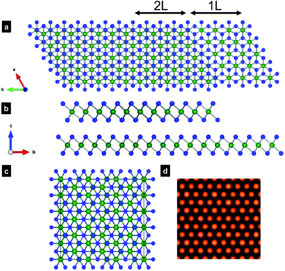
MoSe2 and MoS2 are isostructural, consisting of close-packed Mo atoms sandwiched between two close-packed Se/S atoms. Slab of hexagonally packed Mo atoms and Se/S atoms can be organized into different stacking sequence with totally three different polymorphs. There are two naturally occurring the 2H and 3R phases in which the 2H phase is found to be abundantly present. The 1T phase is a synthetic material, prepared by intercalation or thermal treatment of the 2H phase at 600 °C.28 Fig. 1a illustrates the 2H polymorph with the stacking sequence ABA, regarded as the most stable form of MoSe(S)2.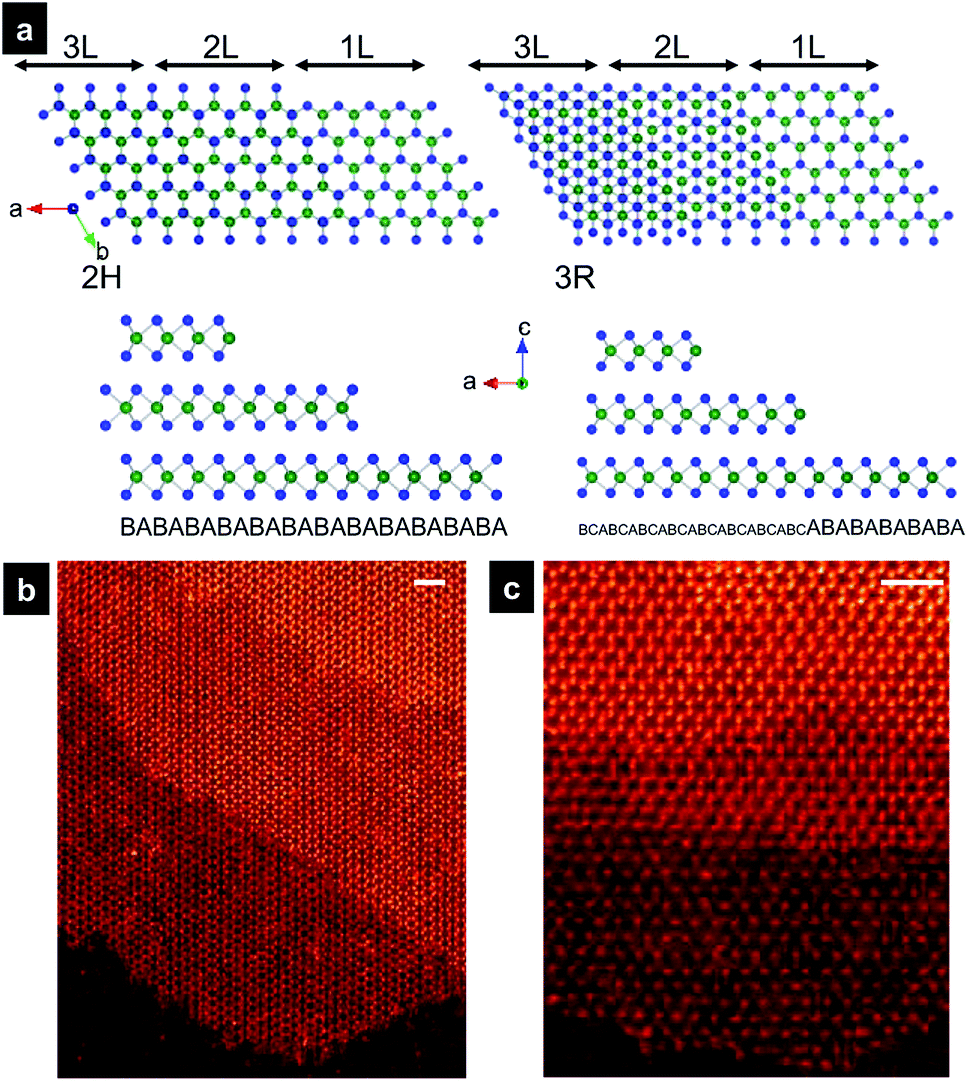 | ||
| Fig. 1 Atomic structure of MoSe2 and MoS2. (a) Crystal structure of MoSe2 2H and 3R phases view along [001] (top) and [010] direction (bottom). (b) HAADF image of exfoliated trilayers MoSe2 in 2H phase viewed along [001] direction. (c) HAADF image of exfoliated trilayers MoS2 in 2H phase viewed along [001] direction. Scale bar, 10 Å. | ||
The few-layer MoSe2 and MoS2 are obtained by exfoliation of commercial bulk materials in the supercritical fluid of dimethylformamide at 400 °C for 1 h.29 During the observation of the exfoliated nanosheets by HAADF-STEM, we observed mainly the 2H polymorph. In Fig. 1b and c, we show HAADF-STEM images viewed from the [001] direction of the trilayers MoSe2 and MoS2 nanosheets, respectively. The contrast of the ADF image is roughly proportional to atomic number Z of imaged species,30,31 with brighter contrast of two stacked Se2 atoms and dimmer contrasts of Mo in monolayer part in Fig. 1b. In HAADF image of monolayer part of MoS2 in Fig. 1c, the Mo (Z = 42) columns have stronger contrast, while the dimmer ones are S (Z = 16) atoms. Three Mo atoms and three Se2/S2 columns form with each other a hexagonal configuration that matches well the illustration in Fig. 1a. Sulfur atoms are visible in the HAADF image, however, the contrast are faint. Since the light elements such as sulfur are barely visible in ADF mode when heavy atoms such as Mo are present.30,31 STEM with probe-forming aberration correctors is a powerful instrument for visualization on the local atomic structure and the chemical composition at the atomic resolution. For thin nanosheet, ADF image contrast intensity varies strongly with the number of atomic on the column, providing direct and accurate tool to measure the thickness of thin samples and to identify chemical composition at various defect sites.
Atomic structure of inversion domains grain boundary
Atomic-scale observation of monolayer MoS2 shows that 60° grain boundary of the 2H and 1T phases can be created due to gliding atomic planes of sulfide and/or molybdenum under electron irradiation.28 Besides that the stacking domains of the 2H and 3R phases have been found in a multilayer MoS2 and MoSe2.18,32 Lu et al. observed the 3R stacking among 2H bilayer MoSe2 stacking growth by CVD method and showed grain boundaries composing of 4|8-fold rings.32 In order to investigate the grain boundaries structure, we describe the dependence of ADF image pattern on phase and number of layer. It notes that the 2H phase of MoSe2 will produce a honeycomb pattern with alternating bright and dim contrast as shown in Fig. 1a and b, while the 3R phase will form hexagonal patterns with visible contrast in the center of hexagonal ring due to presence of Mo atom. Although the honeycomb patterns are observed in the most part of the viewed nanosheets confirming the presence of mainly 2H phase, the hexagonal pattern with additional contrast appears in the center of each hexagonal ring (3R phase) is found occasionally in few cases.In Fig. 2a, we display the HAADF image of the MoSe2 nanosheets with the visualization of the domain grain boundaries of the 2H and 3R phases. The monolayer region (1L) of MoSe2 is readily indentified, located above the blue line. The Se atoms have stronger contrasts, the dimmer ones are Mo atoms as indicated by superimposed atomic arrays. In the bilayer region (2L) located between blue and white lines, the contrast intensities can be seen as honeycomb patterns indicating the presence of 2H bilayer stacking. The trilayer region (3L) is located below the while line. We observe distinct area with different atomic ordering in this bilayer and trilayer regions, located inside the green and yellow lines. The intensity profile taken across the distinct area with gray line is shown in Fig. 2b. The atomic columns associated with Mo (green triangle), Se (blue triangle), and Mo + Se atoms in this phase are identified based on the contrast intensity and line profile are in accordance with previous report.22,32–34 In the intensity profile across the boundary in Fig. 2b, we show appearance of Mo demonstrating presence of 3R phase because the Mo atoms appear in the center of each hexagonal ring. Thus, this evidence clearly reveals the presence of the 3R phase inside the 2H phase in the second layer of MoSe2. The observed area shows the stacking sequence associated with 2H and 3R phases.
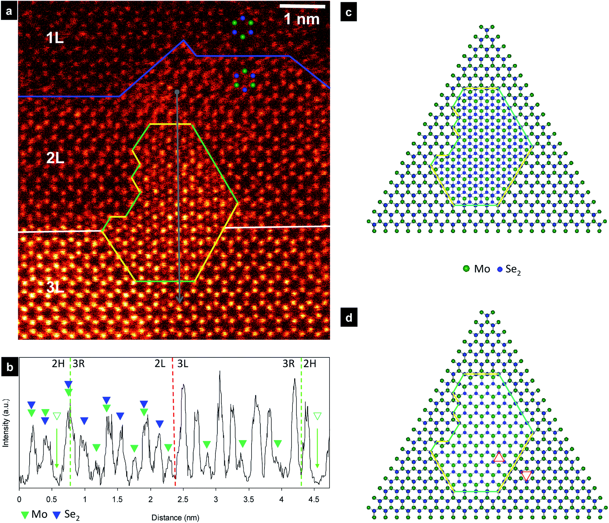 | ||
| Fig. 2 Inversion domains boundary in few-layer MoSe2. (a) HAADF image of MoSe2 with top part is a monolayer, middle part is a bilayer stacking, and bottom part is trilayer stacking, which are separated by blue and while lines. The superimposed atomic arrays on the inset of indicate the locations of atoms in first layer and second layer of 2H phase. The 3R phase appears inside the yellow and green dashed line. (b) Image intensity profile acquired along the gray line in (a). (c) The structure model of the observed region of bilayer stacking. (d) Atomic model of experimental structure of second layer shown in (c). The yellow and green lines indicate the grain boundary composed of 4- and 8-fold rings respectively. Two triangles indicate the orientation of two inversion domains. | ||
On the basic of contrast intensity, the atom columns can be assigned with the structure model depicted in Fig. 2c. In order to visualize the phase boundary clearly, the structure of the second layer is shown in Fig. 2d by removing the first layer, considering that this two phases share the first layers. It is assumed that the first layer is perfect layer without altering of atomic ordering and that the growth defects occurred in the second layer. This assumption is deduced from the fact that when the order of stacking layers change, their simulated contrast and HAADF image pattern do not change as shown in Fig. S1.† The 2H and 3R parts of the monolayer region are mirror symmetric at the lines as illustrated by the two triangles in Fig. 2d. Thus, we observed two types of grain boundaries in the second layer of these inversion domains. The first grain boundaries (denoted as yellow lines) are composed of the chains of 4-fold rings (4|4) with point-sharing at a common Se site. This type of phase boundary has been previously observed in grain boundary of CVD-grown MoSe2,32,33 and molecular beam grown MoSe2,35–37 or in grain boundary of 2H phase,21 or boundary of 2H and 1T phase,28 in MoS2. In contrast, the second grain boundaries (denoted as green lines) comprise of chains of 8-fold rings. Notably, the Se atoms at this 8-fold rings change from the regular 3-fold coordination to 2-fold coordination and Mo atoms retain the regular 6-fold coordination. The growth of such inversed domain in the second layer can be induced by Se vacancy formation,38,39 or trefoil-like point defects.40
It should be noted that Mo at the edge of the 3R phase is relaxed from the center of hexagonal ring, to from the 8-fold rings. This observed region is partly of trilayer stacking, which can be understood by the increase of contrast intensity in Fig. 2b. However, the intensity at the center of hexagonal rings retains unchanged, indicating that the third layer is 2H stacking on the second layer of the 2H phase. In other word, all the Mo atoms of the third layer are stacked on the top of Se2 atoms of the second layer in the 2H region.
In order to reproduce the contrast intensity at the inversion domain boundaries in the experimental HAADF image (see Fig. 2a), we have investigated the IDBs models with monolayer, bilayer, and trilayer by STEM image simulations as shown in Fig. 3a and b. Multislice HAADF STEM image simulations are performed using Dr. Probe package,42 with parameters close to the experimental imaging conditions and using the atomic models relaxed by DFT calculations. Structural models were visualized using VESTA software.43 The atomic positions in all IDBs models are relaxed by DFT calculations. The simulated images agree well with the experimental images that the Mo atoms appear in the center of each hexagonal ring in the 3R region of the bilayer and trilayer MoSe2. In Fig. 3c, we show the contrast at the edges (near the green and yellow lines of Fig. 2a) with the experimental HAADF image and the corresponding simulated image of the bilayer MoSe2. The obtained results confirm that the contrast at the edges is contributed from one layer and not a superposing effect from two layer or reconstructed edges.
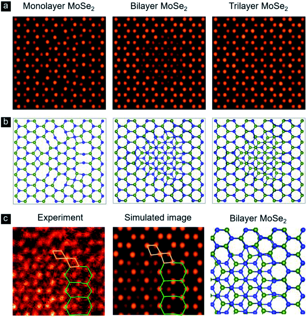 | ||
| Fig. 3 Simulated HAADF-STEM images of the IDBs in monolayer, bilayer, and trilayer MoSe2. (a and b) The figure shows simulated images (a) based on the DFT-optimized structures (b) for the IDBs models. (c) HAADF image and the corresponding simulated image of bilayer MoSe2 showing the 4-fold rings (yellow lines) and 8-fold rings (green lines). | ||
Similarly, stacking region of 2H and 3R phases of MoS2 nanosheets can be observed in some nanosheets. An example is given in Fig. 4 and S2.† The atomic columns form a honeycomb pattern in the bottom region of the image, whereas additional visible contrast appears in the center of each honeycomb in the top region evidenced from image intensity profile in Fig. 4b. The observed area is clearly shown the occurrence of 2H and 3R phases. However, the number of stacking layer is difficult to indentify in this case, hindering the ability to visualize the stacking boundaries in MoS2 nanosheets.
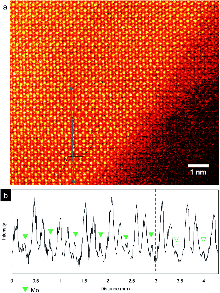 | ||
| Fig. 4 Inversion domains grain boundary in MoS2. (a) HAADF image of MoS2 nanosheets. The dark line indicates the stacking boundaries of 2H and 3R phase. (b) Image intensity profile acquired along the denoted line in (a). The red dashed lines indicate boundary position. | ||
Schematic illustrations of proposed atomic growth model of the inversion domains and their boundary defects are presented in Fig. 5b–f. The inversion domains transition involves interplaying between evolution of Mo–Se bond rotations and Se2 vacancy generation.40 A three-fold rotational defect forms with three pairs of Mo–Se bonds rotating 60° around the Mo atom. Then, the creation of two vacancies of Se pairs at the vicinity of octagons leads to rearrangements into the heterostructure with 8|8 IDBs. The further growth of this distinct IBDs can be processed by controlled electron-beam irradiation on MoSe2 obtained by CVD methods.
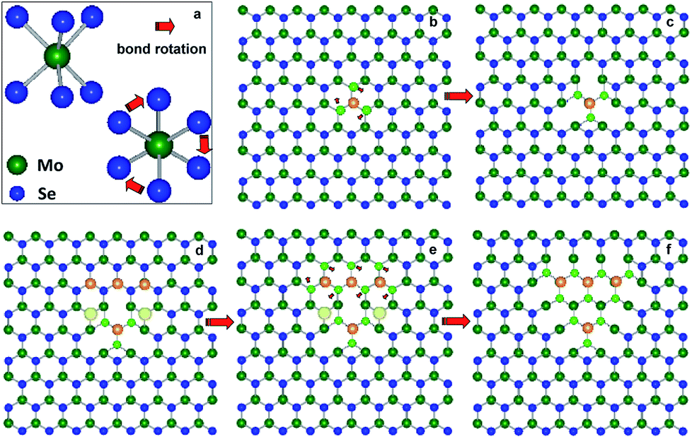 | ||
| Fig. 5 The schematic illustration of the atomic growth of inversion domain. (a) Three-fold rotational defects with Mo–Se bonds rotating 60°; (b) 60° rotation of three pairs of Mo–Se (blue) bonds around the Mo atom (orange); (c) to form three octagons; (d) the creation of two vacancies of Se pairs (yellow) at the vicinity of octagons; (e) seven pairs of Mo–Se bond rotations 60° around the Mo atoms marked by orange color; (f) the heterostructure with 8|8 IDBs. | ||
One may call into question the possibility of 1T domain in this heterostructures. To exclude the presence of 2H–1T junction, we describe the structure of 1T phase and their HAADF image simulation in Fig. 6. The 1T phase shows the atomic stacking sequence of ABC (SeMoSe). Two stack Se atoms are separated and one Se plane occupies center of a 2H hexagonal lattice (Fig. 6a). The simulated HAADF image in Fig. 6d shows that these atomic columns produce equal contrast. Therefore, bilayer of MoSe2 1T phase generates a pattern which is totally different from the observation in Fig. 2. This evidence excludes the 2H → 1T phase transition. In fact, the 2H → 1T phase usually occurs in the exfoliation with lithium intercalation method which induce the S atomic plane gliding.28 Our exfoliation method by supercritical fluid could preserve the trigonal prismatic coordination in 2H or 3R phase.29
 | ||
| Fig. 6 Atomic structure of MoSe2 1T phase and simulated HAADF image. (a) Crystal structure of MoSe2 1T phase view along [001] and (b) [110] direction. (c) Bilayer MoSe2 used to simulate HAADF image and (d) simulated HAADF image of 1T phase. | ||
To further explore the experimental findings, we have carried out first principles calculations of the atomic structures with inversion domain boundaries in the monolayer MoSe2. The IDBs including the alternating chains of 4- and 8-fold rings cannot be make without threefold rotational symmetry in the MoSe2 hexagonal lattice.37 In this study, we thus adopt four supercells to model the IDBs in the monolayer MoSe2, corresponding to 4 × 7, 5 × 8, 5 × 9, and 6 × 10 unit cells of an ideal lattice in a rectangular a√3 × a representation, in which a = 3.327 Å is lattice constant of the monolayer MoSe2. As shown in Fig. 7, we find that after the relaxation, the structures of the IDBs are locally stables at the local minima in energy. The Mo atoms at the 4|4 and 8|8-fold rings retain the 6-fold coordination; however, the Se atom at the 4|4 and 8|8-fold rings changes from the 3-fold coordination to 4-fold coordination and 2-fold coordination, respectively. Interestingly, the Se atoms at the 8-fold rings change their coordination, and their 8-fold rings show the distortion. The distortion of the 8-fold rings can also be observed in the HAADF image in Fig. 3c left. In the cases of the bilayer and trilayer MoSe2; however, the shifts of two sharing Se atoms in the 8-fold rings are difficult to observe clearly in our experiments, since there is a Mo atom under the two Se sharing atoms as shown in Fig. 3c right. The calculated formation energies per unit length of 4|4 and 8|8-fold rings are 0.19 and 0.42 eV Å−1, respectively (please refer to the estimation of formation energy section in ESI† for more details), indicating that the 4|4-fold rings is easily generated. This result is consistent with the fact that 4|4 IDBs is often observed in previous reports.37,38,45
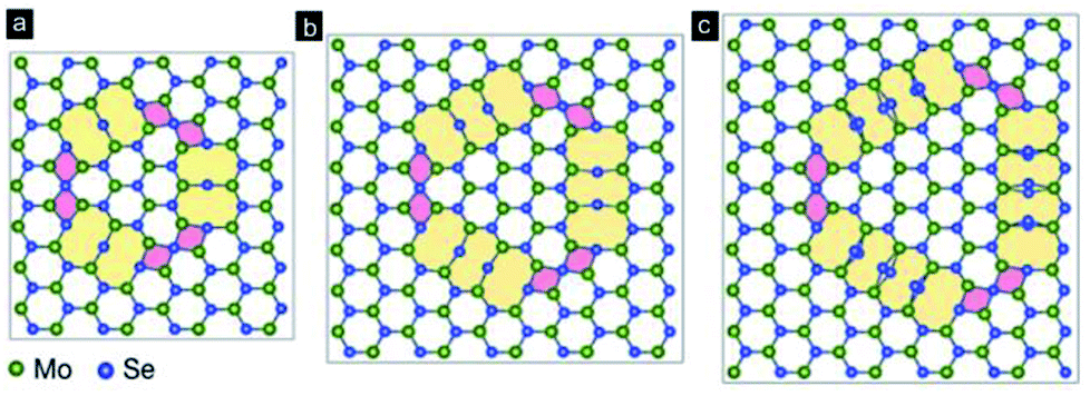 | ||
| Fig. 7 DFT relaxed atomic models of the inversion domain boundaries in the monolayer MoSe2. The solid black boxes represent the 4 × 7, 5 × 8, and 5 × 9 supercells, in which the 8|8-fold rings with two (a), three (b), and four (c) rings, respectively, are displayed in yellow, and the 4|4-fold rings with two rings are displayed in pink. | ||
Recently, Zande et al. showed that the measured in-plane electrical conductivity of the monolayer MoS2 is slightly increased by the mid-gap states of Mo atoms at grain boundaries.20 Therefore, it is important to understand how the 4|4- and 8|8-fold rings contribute to electrical transport in the present IDBs model. Fig. 8 shows the projected density of states (PDOS) with Gaussian broadening of 0.05 eV from Mo and Se atoms at the domain center (Mobulk and Sebulk), the 4|4-fold rings (Mo4|4 and Se4|4), and the 8|8-fold rings (Mo8|8 and Se8|8). The shaded energy region indicates a bandgap about 1.5 eV of the both Mobulk and Sebulk atoms, which is close to the bandgap of a pristine monolayer MoSe2 (∼1.58 eV).41 The PDOS shows mid-gap states at the Fermi energy, EF, that appear mainly in the projected DOS of the Mo4|4 and Mo8|8 atoms in the IDBs as shown in Fig. 8b. Therefore, the IDBs including the alternating chains of 4- and 8-fold rings behave as the one-dimensional metallic chains embedded in the semiconducting monolayer MoSe2 matrix because of the new states at EF. Since the electron states around Fermi energy (EF) are the main contribution to the electrical conductivity and chemical reaction, it is important to realize that the PDOS of the Mo8|8 atom around EF are larger than that of the Mo4|4 atom. Moreover, the PDOS of Se atoms opens the gap at EF by distorting (or the shift) of Se-chain in the 8-fold boundary as shown in Fig. 8a and c. This shift is a kind of the Peierls instability44 for one-dimensional Se chain with high symmetry.
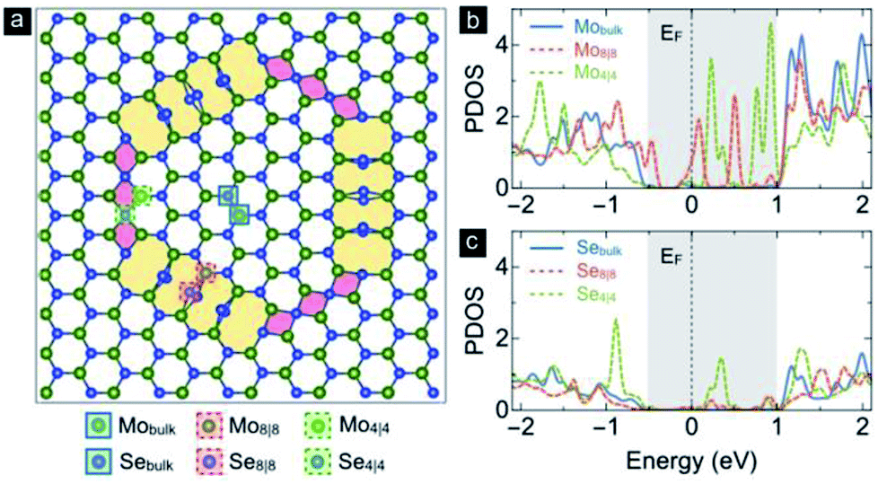 | ||
| Fig. 8 DFT calculated the projected density of states (PDOS) from the domain center and the inversion domain boundaries in the monolayer MoSe2. The PDOS were acquired from Mo (b) and Se atoms (c) marker in blue (domain), red (8|8-fold rings), and green (4|4-fold rings) boxes shown in the 6 × 10 supercell (a). | ||
A combination of STEM Z-contrast and image simulation with DFT calculation points to 4|4-fold rings chains and 8|8-fold rings chains as IDB defects. These 4|4-fold rings chains in the boundaries of 2H/3R phases can be found in MoSe2 bilayers grown by CVD method.45 In a recent report, Zhao et al. have identified the domain boundaries of 2H/3R in bilayer MoSe2 by HAADF imaging and image simulation. Our results provide additional insight into the 8|8-fold rings chains in this type of domain boundaries and predict electronic properties and particularly the electronic transport properties, as we have found their one-dimensional metallic chains behavior and larger PDOS of the Mo8|8 atom around EF.
4. Conclusion
In summary, atomic-resolved imaging structure of few-layer MoSe2 provides a view into grain boundaries of inversion domains. The grain boundaries are identified, comprising of the alternating chains of 4-fold ring and 8-fold ring. The appearance of 8|8-fold rings (Mo8|8) chains may significantly influence the electronic properties and particularly the electronic transport properties, as we have found their one-dimensional metallic chains behavior and larger PDOS of the Mo8|8 atom around EF. The atomic-resolved structural analysis and DFT calculation in present work provide understanding on chemical environment and coordination in the inversion domain boundary, which provides new opportunities to explore the novel material properties via engineering the defects.Conflicts of interest
There is no conflicts of interest to declare.Acknowledgements
This research work was financially supported by Japan Society for Promotion of Science (JSPS, Grant No. PU15903), Funding Program for World-Leading Innovative R&D on Science and Technology (FIRST) and Core Technology Consortium for Advanced Energy Devices, Tohoku University, Japan. The work was partially supported by ALCA-SPRING (ALCA-Specially Promoted Research for Innovative Next Generation Batteries) from Japan Science and Technology Agency (JST). N. T. Hung acknowledges JSPS KAKENHI Grants No. JP18J10151. R. S. acknowledges JSPS KAKENHI Grants No. JP18H01810.Notes and references
- M. Chhowalla, H. S. Shin, G. Eda, L. J. Li, K. P. Loh and H. Zhang, Nat. Chem., 2013, 5, 263–275 CrossRef PubMed.
- Y. Yu, S. Y. Huang, Y. Li, S. N. Steinmann, W. Yang and L. Cao, Nano Lett., 2014, 14, 553–558 CrossRef CAS PubMed.
- D. R. Allan, A. A. Kelsey, S. J. Clark, R. J. Angel and G. J. Ackland, Phys. Rev. B: Condens. Matter Mater. Phys., 1998, 57, 5106–5110 CrossRef.
- K. F. Mak, C. Lee, J. Hone, J. Shan and T. F. Heinz, Phys. Rev. Lett., 2010, 105, 136805 CrossRef PubMed.
- C. T. Tye and K. J. Smith, Top. Catal., 2006, 37, 129–135 CrossRef CAS.
- D. Voiry, H. Yamaguchi, J. Li, R. Silva, D. C. Alves, T. Fujita, M. Chen, T. Asefa, V. Shenoy and E. Eda, Nat. Mater., 2013, 12, 850–855 CrossRef CAS PubMed.
- H. Y. Chang, S. Yang, J. Lee, L. Tao, W.-S. Hwang, D. Jena, N. Lu and D. Akinwande, ACS Nano, 2013, 7, 5446–5452 CrossRef CAS PubMed.
- Q. He, Z. Zeng, Z. Yin, H. Li, S. Wu, X. Huang and H. Zhang, Small, 2012, 8, 2994–2999 CrossRef CAS PubMed.
- X. P. Hong, J. H. Kim, S. F. Shi, Y. Zhang, C. H. Jin, Y. H. Sun, S. Tongay, J. Q. Wu, Y. F. Zhang and F. Wang, Nat. Nanotechnol., 2014, 9, 682–686 CrossRef CAS PubMed.
- K. Chang and W. X. Chen, Chem. Commun., 2011, 47, 4252–4254 RSC.
- K. Chang and W. X. Chen, ACS Nano, 2011, 28, 4720–4728 CrossRef PubMed.
- Y. Liang, R. Feng, S. Yang, H. Ma, J. Liang and J. Chen, Adv. Mater., 2011, 23, 640–643 CrossRef CAS PubMed.
- J. N. Coleman, M. Lotya, A. O'Neill, S. D. Bergin, P. J. King, U. Khan, K. Young, A. Gaucher, S. De and R. J. Smith, et al., Science, 2011, 331, 568–571 CrossRef CAS PubMed.
- R. J. Smith, P. J. King, M. Lotya, C. Wirtz, U. Khan, S. De, A. O'eill, G. S. Duesberg, J. C. Grunlan and G. Moriarty, Adv. Mater., 2011, 23, 3944–3948 CrossRef CAS PubMed.
- A. O'Neill, U. Khan and J. N. Coleman, Chem. Mater., 2012, 24, 2414–2421 CrossRef.
- G. Cunningham, M. Lotya, C. S. Cucinotta, S. Sanvito, S. D. Bergin, R. Menzel, M. S. P. Shaffer and J. N. Coleman, ACS Nano, 2012, 6, 3468–3480 CrossRef CAS PubMed.
- K. R. Paton, E. Varrla, C. Backes, R. J. Smith, U. Khan, A. O'Neill, C. Boland, M. Lotya, O. M. Istrate and P. J. King, et al., Nat. Mater., 2014, 13, 624–630 CrossRef CAS PubMed.
- A. Shmeliov, M. Shannon, P. Wang, J. S. Kim, E. Oknishi, P. D. Nellist, K. Dolui, S. Sanvito and V. Nicolisi, ACS Nano, 2014, 8, 3690–3699 CrossRef CAS PubMed.
- S. Najmaei, Z. Liu, W. Zhou, X. Zou, G. Shi, S. Lei, B. I. Yakobson, J. C. Idrobo, P. M. Ajayan and J. Lou, Nat. Mater., 2013, 12, 754–759 CrossRef CAS PubMed.
- A. M. van der Zande, P. Y. Huang, D. A. Chenet, T. C. Berkelbach, Y. You, G. H. Lee, T. F. Heinz, D. R. Reichman, D. A. Muller and J. C. Hone, Nat. Mater., 2013, 12, 554–561 CrossRef CAS PubMed.
- W. Zhou, X. Zou, S. Najmaei, Z. Liu, Y. Shi, J. Kong, J. Lou, P. M. Ajayan, B. I. Yakobson and J.-C. Idrobo, Nano Lett., 2013, 13, 2615–2622 CrossRef CAS PubMed.
- X. Wang, Y. Gong, G. Shi, W. L. Chow, K. Keyshar, G. Ye, R. Vajtai, J. Lou, Z. Liu, E. Ringe, B. K. Tay and P. M. Ajayan, ACS Nano, 2014, 8, 5125–5131 CrossRef CAS PubMed.
- J. Hong, Z. Hu, M. Probert, K. Li, D. Lv, X. Yang, L. Gu, N. Mao, Q. Feng, L. Xie, J. Zhang, D. Wu, Z. Zhang, C. Jin, W. Ji, X. Zhang, J. Yuan and Z. Zhang, Nat. Commun., 2015, 6, 6293 CrossRef CAS PubMed.
- S. Wang, G.-D. Lee, S. Lee, E. Yoon and J. H. Warner, ACS Nano, 2016, 10, 5419–5430 CrossRef CAS PubMed.
- T. Ozaki, et al., 2009, https://www.openmx-square.org/.
- T. Ozaki and H. Kino, Phys. Rev. B: Condens. Matter Mater. Phys., 2004, 69, 195113 CrossRef.
- J. P. Perdew, K. Burke and M. Ernzerhof, Phys. Rev. Lett., 1996, 77, 3865 CrossRef CAS PubMed.
- Y.-C. Lin, D. O. Dumcenco, Y.-S. Huang and K. Suenaga, Nat. Nanotechnol., 2014, 9, 391–396 CrossRef CAS PubMed.
- Q. D. Truong, M. K. Devaraju, Y. Nakayasu, N. Tamura, Y. Sasaki, T. Tomai and I. Honma, ACS Omega, 2017, 2, 2360–2367 CrossRef CAS.
- P. D. Tran, T. V. Tran, M. Orio, S. Torelli, Q. D. Truong, K. Nayuki, Y. Sasaki, S. Y. Chiam, R. Yi, I. Honma, J. Barber and V. Artero, Nat. Mater., 2016, 15, 640–646 CrossRef CAS PubMed.
- Q. D. Truong, M. K. Devaraju, D. N. Nguyen, Y. Gambe, K. Nayuki, Y. Sasaki, P. D. Tran and I. Honma, Nano Lett., 2016, 16, 5829–5835 CrossRef CAS PubMed.
- X. Lu, M. I. B. Utama, J. Lin, X. Gong, J. Zhang, Y. Zhao, S. T. Pantelides, J. Wang, Z. Dong, Z. Liu, W. Zhou and Q. H. Xiong, Nano Lett., 2014, 14, 2419–2425 CrossRef CAS PubMed.
- J. Lin, S. T. Pantelides and W. Zhou, ACS Nano, 2015, 9, 5189–5197 CrossRef CAS PubMed.
- C. Huang, S. Wu, A. Sanchez, J. Peters, R. Beanland, J. Ross, P. Rivera, W. Yao, D. Cobden and X. Xu, Nat. Mater., 2014, 13, 1096–1101 CrossRef CAS PubMed.
- Y. Ma, H. C. Diaz, J. Avila, C. Chen, V. Kalappattil, R. Das, M. H. Phan, T. Cadez, J. M. P. Carmelo, M. C. Asensio and M. Batzill, Nat. Commun., 2017, 8, 14231 CrossRef CAS PubMed.
- Y. Ma, S. Kolekar, H. C. Diaz, J. Aprojanz, I. Miccoli, C. Tegenkamp and M. Batzill, ACS Nano, 2017, 11, 5130–5139 CrossRef CAS PubMed.
- J. Hong, C. Wang, H. Liu, X. Ren, J. Chen, G. Wang, J. Jia, M. Xia, C. Jin, W. Ji, X. Zhang, J. Yuan and Z. Zhang, Nano Lett., 2017, 17, 6653–6660 CrossRef CAS PubMed.
- O. Lehtinen, H.-P. Komsa, A. Pulkin, M. B. Whitwick, M.-W. Chen, T. Lehnert, M. J. Mohn, O. V. Yazyev, A. Kis and U. Kaiser, ACS Nano, 2015, 9, 3274–3283 CrossRef CAS PubMed.
- S. Wang, G.-D. Lee, S. Lee, E. Yoon and J. H. Warner, ACS Nano, 2016, 10, 5419–5430 CrossRef CAS PubMed.
- Y.-C. Lin, T. Bjorkman, H. P. Komsa, P. Y. Teng, C. H. Yeh, F. S. Huang, K. H. Lin, J. Jadczak, Y.-S. Huang, P. W. Chiu, A. Krasheninnikov and K. Suenaga, Nat. Commun., 2015, 6, 6736 CrossRef CAS PubMed.
- Y. Zhang, T. R. Chang, B. Zhou, Y. T. Cui, H. Yan, Z. Liu, F. Schmitt, J. Lee, R. Moore, Y. Chen and H. Lin, Nat. Nanotechnol., 2014, 9, 111–115 CrossRef CAS PubMed.
- J. Barthel, Ultramicroscopy, 2018, 193, 1–11 CrossRef CAS PubMed.
- K. Momma and F. Izumi, J. Appl. Crystallogr., 2011, 44, 1272–1276 CrossRef CAS.
- C. Kittel, Introduction to solid state physics, 8th edn, Wiley, 1996 Search PubMed.
- X. Zhao, Z. Ding, J. Chen, J. Dan, S. M. Poh, W. Fu, S. J. Pennycook, W. Zhou and K. P. Loh, ACS Nano, 2018, 12, 1940–1948 CrossRef CAS PubMed.
Footnotes |
| † Electronic supplementary information (ESI) available: Structural illustration, more HAADF-STEM images. See DOI: 10.1039/c8ra07205a |
| ‡ These authors contributed equally to this work. |
| This journal is © The Royal Society of Chemistry 2018 |