
 Open Access Article
 This Open Access Article is licensed under a Creative Commons Attribution-Non Commercial 3.0 Unported Licence
The influence of the morphological characteristics of nanoporous anodic aluminium oxide (AAO) structures on capacitive touch sensor performance: a biological application†
J. O. Carneiro *a,
F. Machadoa,
M. Pereiraa,
V. Teixeiraa,
M. F. Costaa,
Artur Ribeirob,
Artur Cavaco-Paulob and
A. P. Samantilleke*a
*a,
F. Machadoa,
M. Pereiraa,
V. Teixeiraa,
M. F. Costaa,
Artur Ribeirob,
Artur Cavaco-Paulob and
A. P. Samantilleke*a
aCentre of Physics, University of Minho, Azurém Campus, 4800-058 Guimarães, Portugal. E-mail: carneiro@fisica.uminho.pt; anura@fisica.uminho.pt
bCentre of Biological Engineering, University of Minho, Gualtar Campus, 4710-057 Braga, Portugal
First published on 6th November 2018
Abstract
This work is devoted to the study of the influence of different anodic aluminium oxide (AAO) morphologies on the sensitivity and performance of an AAO-based capacitive touch sensor. The AAO structures were fabricated in a cylindrical homemade anodization cell made from a solid polycarbonate billet via a lathe machining process. The AAO morphologies were obtained from the anodization of Al foil by using three different types of electrolyte (sulphuric acid, oxalic acid and phosphoric acid) and their morphologies are reported and compared using scanning electron microscopy (SEM) micrographs and current–time characteristic curves. The sensors were fabricated by integrating the AAO structure with a nanotextured gold thin film deposited over the AAO layer by thermal evaporation, thus realizing a type of metal/insulator/metal parallel-plate capacitance sensor. It is demonstrated that AAO morphologies have influence on the performance of the AAO-based capacitive touch sensors. The variation of the capacitance of the sensors is investigated in this work for the AAO structures produced from anodization in an attempt to select anodizing conditions for a biological application aiming to detect small microorganisms such as bacterial colonies of Escherichia coli.
1. Introduction
The industrialization of the anodizing process arose in the mid-1920s, after Buff1 have demonstrated the possibility of oxidizing metallic aluminium using an electrochemical process carried out in acid aqueous solution, which led to the formation of an oxide layer much thicker than that of its thin natural passive layer. Since then, the application of anodized Al and its alloys has continued to grow, as the anodizing process offers the anodized product a number of unique engineering protection properties such as excellent corrosion, hardness, and abrasion resistance.2 Since anodic aluminium oxides (AAOs) showed high porosity, they have been also employed in industry as good adhesion platforms for electroplating, painting and decorative coloration, in the form of colourful anodizing where applications to car tuning finds its greatest expression. Furthermore, anodized products can be found in applications such as special injection moulds, various electronic devices, cookware sets, automotive parts, window frames for buildings, and several types of machine components, among others. In many ways, it is noteworthy that almost a century after the observation of Al anodizing, this phenomenon has recently triggered interest and acquired increased importance to the scientific community that works in leading scientific areas such as the field of nanotechnology. This trajectory was commenced with the work developed by Masuda and Fukuda,3 who in 1995, reported the production of porous AAO layers exhibiting a self-ordered pore structure and one year later Masuda and Satoh4 developed, what is known as two-step anodizing process by which porous AAO could be obtained with improved structural periodicities over larger spatial areas. AAOs find many high-tech applications in nanostructures and devices. Among different research areas, the use of AAO in one-dimensional nanostructures is noteworthy,5–11 as tubular membranes for hemodialysis,12,13 membranes for gas separation, drug delivery and bone fixation14–17 energy storage devices, among others.18–21 Recent work by several authors12,14 prove that nanostructured functional layers of significantly enlarged surface areas for sensor applications can be made from thin porous alumina films.The fabrication of AAO is based on simple, cost-effective self-ordering anodization of aluminium, which yields vertically aligned, highly ordered nanoporous structures.
It is well known that there are two main processes for AAO fabrication, namely mild anodization (MA) and hard anodization (HA).3,22 In general both of these processes utilize three different types of acidic electrolytes, namely sulphuric, oxalic, and phosphoric acids. The MA process has been mostly used in academic work for a wide variety of nanotech applications. However, since MA uses a low anodizing potential, the growth rate of AAO nanostructures is in general slow, and the process becomes even more time consuming under the two-step anodizing conditions. On the contrary, HA is mostly used by certain industrial applications due to efficient growth of AAO nanostructures and improved periodicity of nanopores over larger spatial areas. HA process requires the application of relatively high anodic voltages, thus leading to a high current density, which causes the HA process to have exothermic characteristics (as the result of Joule's heating). However, the generation of excessive heat during HA processes is also responsible for the acidic dissolution of the formed AAO nanoporous structure as well as strongly contributing to the occurrence of local breakdown,23 for which reason the fabrication of AAO nanostructures under HA conditions has not been widely used in nanotechnology applications. Several approaches have been made to find effective solutions to extract the reaction heat such as the use of cooling systems24 or certain cooling reagents (e.g. ethanol is used as coolant agent) added to the aqueous electrolytes in order to compensate or minimize the generated heating and local burning problems.25,26 In recent years, capacitive type tactile or pressure sensors have been reported.27,28 Hong et al.29 used AAO structures to serve as template to form a nanotextured gold film to fabricate a capacitive touch sensor to detect small contact forces, such as insects. The AAO structures were formed by two-step anodizing conditions from an aqueous solution of 0.3 M oxalic acid at a voltage of 47 V DC. According to the authors, they obtained an AAO structure with an average nanopore diameter of 54 nm and a porosity of about 23.6%. After covering the entire pore structure by a nanotextured Au top electrode, they registered a capacitance of ∼1.75 nF and an average capacitance variation of 4.1%.
Taking as basis the study performed by Hong et al., we have performed a experimental campaign in which the main objective and novelty is to study the influence of different AAO morphologies, obtained by using three different acid electrolytes and anodization conditions, on the sensitivity and performance of an AAO-based capacitive touch sensor. The sensor fabricated proved to be able to detect the surface contact interaction of small objects (bacterial colonies of Escherichia coli and also a tiny metal plate were used in this work), due to variations on the nanotextured Au electrode area. Escherichia coli (E. coli) is particularly interesting in this study as capacitive sensors of this nature generally show high selectivity and is able to distinguish E. coli when present together with competing bacterial strains, which are known to have similar shape.28 Idil et al. also reported suitability of similar capacitive touch sensors for the detection of E. coli, having investigated selectivity of the E. coli-imprinted electrode with other bacterial strains such as Staphylococcus aureus (S. aureus), Bacillus subtilis (B. subtilis), and Salmonella paratyphi (S. paratyphi) using real-time detection experiments.30
The performance of the AAO capacitive-type sensor and its dependence on the AAO morphology, which is characterized by different structural parameters such as inter-pore distance (Dint), pore diameter (Dp) and porosity (P), which in turn, are dependent on the anodizing conditions, namely the electrolyte type, concentration, temperature, applied anodizing potential and anodizing time will be investigated in this work.
2. Sensing principle and mechanism of the AAO capacitive-type sensor
The underlying physical principle that governs the practical performance of the AAO capacitive sensor, is associated with the variation of capacitance, which results from changes on the AAO surface area (due to the contact with the object) and also on the properties of the dielectric medium. Under the scope of this work, the presence of small objects was simulated via the use of a specific bacterial culture medium that clearly demonstrated a strong capability of the as-fabricated AAO-based capacitive device to be used in biomedical applications, such as in hypothetical scenarios where someone, over time, intends to monitor the progression stage of a particular type of bacterial disease.Fig. 1 refers to the underlying concept of a nanoporous AAO capacitive sensor. The AAO structure is grown through the anodization process from a pure aluminium substrate. The structural properties (i.e. Dint and P), of the obtained AAO structures depends on the type of electrolytes used, namely sulphuric, oxalic, and phosphoric acids.
 | ||
| Fig. 1 Nanoporous AAO structure used as a capacitive-type sensor; (a) schematic representation of the metal–insulator–metal (MIM) sensor architecture comprising the nanotextured thin film Au top electrode, the nanoporous AAO insulator layer and the bottom Al substrate; (b) cross section and top surface of the MIM based AAO capacitive sensor showing main structural characteristics and (c) operating mechanism of the AAO base capacitive sensor when a particular object (e.g. a colony of specific bacteria) makes a contact with the surface of the MIM sensor. | ||
Analysing Fig. 1(a), it is possible to identify the nanotextured top electrode, which is composed of an Au thin film directly deposited on the AAO porous layer by thermal resistive evaporation. The evaporation parameters are presented later in the text. Fig. 1(b) depicts the metal–insulator–metal (MIM) capacitor device, which consists of a base metal (Al) substrate, an insulator (AAO layer) and a top metallic electrode (Au). The sensor operating mechanism can be briefly described as follows: due to the AAO nanoporous structure, which may have different structural properties according the type of used electrolyte, any external object (in this work, bacteria and also an Al metal disk) that could enter into contact with the surface of the MIM device will cover the surface pores to some extent, thus causing a variation on the total electrical capacitance of the MIM device (see Fig. 1(c)). This occurs because, as soon as the object contacts the nanotextured surface to cover new pores, it creates additional capacitors (where the dielectric medium is air or a particular aqueous medium in the case of the bacteria culture), which adds a parallel capacitive component to the existing MIM device and thus, an increase of the total capacitance of the MIM device is expected. In this work the E. coli was used as a model microorganism to assess and validate the ability of the AAO based sensors to detect microorganisms.
3. Experimental
3.1 Fabrication technology: production of AAO nanoporous structures by Al anodization
The nanoporous AAO structures were electrochemically produced from Al (99.999% purity) foils (0.25 mm thick, acquired from Sigma-Aldrich) by one-step anodizing process. The anodizing process was realized in a homemade anodization cell comprising an anode (pre-treated Al foil) and a cathode (Pb plate). The body of the electrochemical cell is made of polypropylene material and has a cylindrical geometry fabricated by lathe machining a solid polycarbonate billet.The total volume of the anodization cell is about 220 ml, where the anode is placed at the bottom and holds a circular geometry with a diameter of 20 mm. The cathode consists of one Pb plate with rectangular-type geometry and dimensions of (105 × 15 × 4) mm. Some geometrical details related with the homemade anodization cell are properly identified in the ESI (Fig. SI1(a) and (b)†).
After standard substrate cleaning, the Al foils were subjected to a pre-treatment by ultra-sonication in ethanol/benzine for 10 to 15 minutes at room temperature (RT). The Al foils were then dried and used as anodes in the anodization cell. In order to obtain AAO structures with different structural parameters, the Al foils were anodized with the three different electrolytes: sulphuric acid (0.3 M), oxalic acid (0.3 M) and phosphoric acid (0.3 M). In the case of sulphuric acid and oxalic acid electrolytes, the anodizing process was realized at room temperature (RT) and we observed that the optimum anodizing potential (U) to achieve the best ordering of pores are 21 and 40 V, respectively. For the phosphoric acid electrolyte (HA conditions), the applied anodization potential was U = 150 V at a temperature of 0 °C. All the Al foils were only subjected to one anodizing step by using an EA-PS 3150-04B-power supply (from Elektro Automatik). The current transients, I(t), were monitored during the anodization process using a EA-UTA 12 analogue interface (from Elektro-Automatik) equipped with LabView software. The experimental conditions and the related samples' identification (sample ID) are shown in Table 1.
| Anodizing condition | Sample ID | Electrolyte type/concentration [M] | Electrolyte temperature (°C) | Applied voltage (V) | Anodizing time (min) |
|---|---|---|---|---|---|
| MA | SU | 0.3 M H2SO4 | RT | 21 | 60 |
| OX | 0.3 M H2C2O4 | 40 | 40 | ||
| HA | P1 | 0.3 M H3PO4 | 0 | 150 | 0.67 |
| P2 | 1.08 |
3.2 Deposition of a nano-textured Au top electrode
The deposition of the Au thin film was carried out by resistive thermal evaporation. The thermal evaporating system (ESI, Fig. SI2(a)†) includes a deposition chamber with a volume of 3.8 L, a primary rotary pump (with a pumping speed of 5000 L h−1) and a diffusion pump with a pumping speed of 110 L s−1. The Au thermal evaporation was carried out in order to transfer a nano-textured gold circular top electrode with a radius of 3.75 mm to the AAO surface and connected to a gate with a length of 5 mm. To serve this purpose, a specific mask fabricated from an Al sheet, whose geometry is shown in Fig. SI2(b) and (c),† was used.Taking into account the experimental conditions specified in Table 1, AAO structures with different structural parameters were obtained. The amount of Au wire mass used varied according to the AAO pore diameter, namely 34, 17 and 7 mg for samples identified according to the electrolytes used in deposition, as SU (sulphuric), OX (oxalic), P1 and P2 (phosphoric), respectively. For all of the produced samples, the gold top electrode was evaporated from a 0.5 mm diameter Au wire placed in a tungsten boat (see Fig. SI2(a)†).
Complete evaporation of Au film to the nanoporous AAO surface was attained by firstly evacuating the vacuum chamber to achieve a pressure of 2 × 10⁻⁶ mbar and then applying a current of 220 A and a voltage of 1.2 V for 2 min to the tungsten boat.
It is important to note that each of the fabricated AAO samples were subjected to two consecutive Au thermal evaporation stages. In the first stage, the mask pattern was totally transferred to the surface of the nanoporous AAO structure. The second Au evaporation stage was only performed over the gate by covering the circular region of the mask by a metal disk with a 3.75 mm radius, (as schematized in Fig. SI3(a) of the ESI†). The purpose of this procedure was to obtain an Au top electrode having a nanotextured surface and circular geometry, which in turn is directly linked to a compact gate. All the electrical connections with the Au top electrode were performed by placing a small needle on the surface of the gate pad (see Fig. SI3(b)†). The Al substrate, which supports the AAO structure, acts as the bottom electrode to which, a copper wire was subsequently attached using silver paint.
3.3 Preparation of a bacteria culture as agents for touch sensing tests
A bacterial suspension was employed to demonstrate the capability of an AAO-based parallel-plate capacitor act as an effective capacitive touch sensor. In standard molecular microbiological procedures, Lysogeny Broth (LB) (Grisp, Portugal) is used as liquid medium in qualitative procedures for the growth, cultivation and maintenance of recombinant Escherichia coli strains. In this work, the biological tests were only realized over the AAO structures fabricated from the anodization process using phosphoric acid electrolyte for 0.67 min (corresponding to the AAO sample coded as P1, according to Table 1). The reason why we selected the AAO – P1 sample to perform the biological tests is because this sample showed the best capacitive response arising from the contact with an Al metallic disk that covered the entire surface area of the anodized samples.In order to perform biological tests, a pre-inoculum of E. coli BL21(DE3) was prepared in LB medium and the bacterial culture was grown overnight at 37 °C with constant stirring at 200 rpm. The initial optical density of the medium was adjusted to OD600nm = 0.1. In fact, it is important to emphasize that the medium optical density is directly related to the amount of E. coli present in the bacterial suspension. Then, the AAO-P1 samples, previously disinfected with increasing concentrations of ethanol, were fully dipped in the culture medium with E. coli and were incubated at 37 °C without agitation. Afterwards, the AAO-P1 samples were withdrawn from the bacterial culture medium at different time intervals, namely 1, 4 and 8 hours, and the sensors were coded as A1, A4 and A8, respectively. These time intervals match the times for the E. coli growth and thus, it is expected that within these different time periods, the bacterial colony will multiply due to the conditions provided by the culture medium. Another sensor coded as AC, which is a control sensor, immersed only in the liquid LB medium without E. coli, was also considered. Then, the sensors were subjected to a drying process in an oven at 40 °C for 1 h, and subsequently connected to the LCR meter (QuadTech 1920 Precision LCR Meter) in order to record variations on their capacitive response resulting from changes in the nanotextured surface area of the Au top electrode due to the presence of E. coli. The experimental sequence is schematically shown in Fig. SI4 of ESI.† The performance of the AAO-based capacitive touch sensors was monitored via a capacitance–time plot and the AAO-P1 samples with and without E. coli were observed by scanning electron microscopy (SEM).
3.4 Morphological characterization of AAO samples
The morphology and thickness of all fabricated AAO structures were analysed by scanning electron microscopy (SEM) using a FEI Quanta 400FEG ESEM/EDAX Genesis X4M. The SEM micrographs were subsequently exported to a commercial image-processing program, ImageJ, in order to calculate the AAOs structural parameters, namely porosity, pore diameter, inter-pore distance and pore density.4. Results and discussion
4.1 Current–time characteristics and AAO morphology
The Fig. 2(a) and (b) show the current–time characteristic behaviour of the AAO samples P1 and P2 fabricated under hard anodizing conditions, according to Table 1. | ||
| Fig. 2 Current–time plot related to anodized sample P1 and P2. (a) The current intensity for sample P1 shows two main regions – R1, showing a sharp drop in current intensity and region R2, with a steady current intensity; and (b) the current intensity for sample P2 behaved almost identical to the P1 for the first 60 s (t = 60 s). The main difference of the current profiles is that from t = 60 s (region R3) a sharp increase of the current intensity was observed for the sample P2. | ||
The typical behaviour of I(t) characteristic curves are well-described elsewhere.31–34 From Fig. 2(a) it is possible to distinguish three main regions (R1 and R2). Briefly, at an initial stage (region R1) the current intensity decreases rapidly with time since it is related to the formation of a thin aluminium oxide barrier layer, which should form immediately after the start of the anodizing process.31–34
The current intensity then increases slightly reaching a local maximum. At this stage, the barrier layer experiences a thinning process until it reaches a stable thickness and, simultaneously, the pore formation is initiated on the convex surface due to the increase of the local electric field. In region R2, the current intensity reaches a steady value, which is related to the growth of the porous layer.
On the other hand, from the current–time characteristic curve the thickness h of the formed AAO structure can be estimated by applying the Faraday's law,35
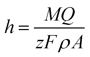 | (1) |
![[thin space (1/6-em)]](https://www.rsc.org/images/entities/char_2009.gif) 485 C mo1−1), Q is the total electrical charge passing in the anodizing process and M and ρ are the molar mass and density of alumina, respectively. The total electrical charge
485 C mo1−1), Q is the total electrical charge passing in the anodizing process and M and ρ are the molar mass and density of alumina, respectively. The total electrical charge 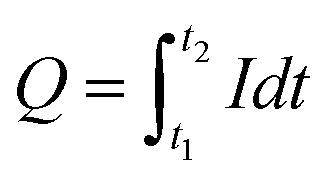 is the integral of current with respect to time, which can be calculated from the experimental I(t) characteristic curve. The thickness of sample P1, determined by eqn (1), is about 5.54 μm, which is a reasonably value close to the one measured by SEM (≈6.3 μm), as shown in Fig. 3(a), which refers to the side view micrograph of sample P1.
 | ||
| Fig. 3 SEM micrographs of AAO nanostructures fabricated under hard anodizing conditions; (a) and (b) are side and top view micrographs for sample P1, respectively whereas (c) and (d) are the side and top view micrographs for sample P2, respectively. | ||
The analysis of SEM micrographs presented in Fig. 3(a) and (b) reveals that, in general, the sample P1 holds a morphology characterized by a well-defined and self-ordered porous alumina. The AAO structure of the sample P1 has an average nanopore diameter and inter-pore distance of ∼183 nm and 294.8 nm, respectively.
I(t) characteristic plot of sample P2, (Fig. 3(b)) shows that after t = 60 s, there was a sharp increase in current intensity (region R3) resulting in a strong local temperature rise due to Joule heating. It has been pointed out that generated heat plays an important role in the enlargement of the pore size by assisting dissolution of the oxide from pore walls, resulting in truncated pore channels.36 This behaviour can be clearly confirmed by the observation of Fig. 3(c) and (d), which correspond to side and top view of the SEM micrographs for sample P2, respectively. The inset shown in Fig. 6(d) is a photographic image of the anodized surface for sample P2, which experienced a “local burning” due to Joule heating. It is possible to observe a damaged and quite irregular surface, which results from the collapse of the pores. It is important to note that although sample P2 does not appear to be useful for the main goal of this work, the destruction of its AAO structure due to pore collapse has led to the formation of alumina nanofibres, which may be of great interest to several other nanotech applications. The process reveals an efficient and economical method to produce Al2O3 nanofibres.
The SEM micrographs presented in Fig. 4(a–c) show the side view of the typical nanotextured Au-AAO-Al (MIM) parallel-plate capacitor referring to samples SU, OX and P1, respectively. The insets shown in Fig. 4(a) and (b) correspond to the SEM top view micrographs of non-textured Au anodized samples SU and OX, respectively (i.e. before thermal evaporation of gold). On the other hand, the inset shown in Fig. 4(c) is the photographic image of sample P1, which reveals the general appearance of its Au nanotextured surface area (Au top electrode).
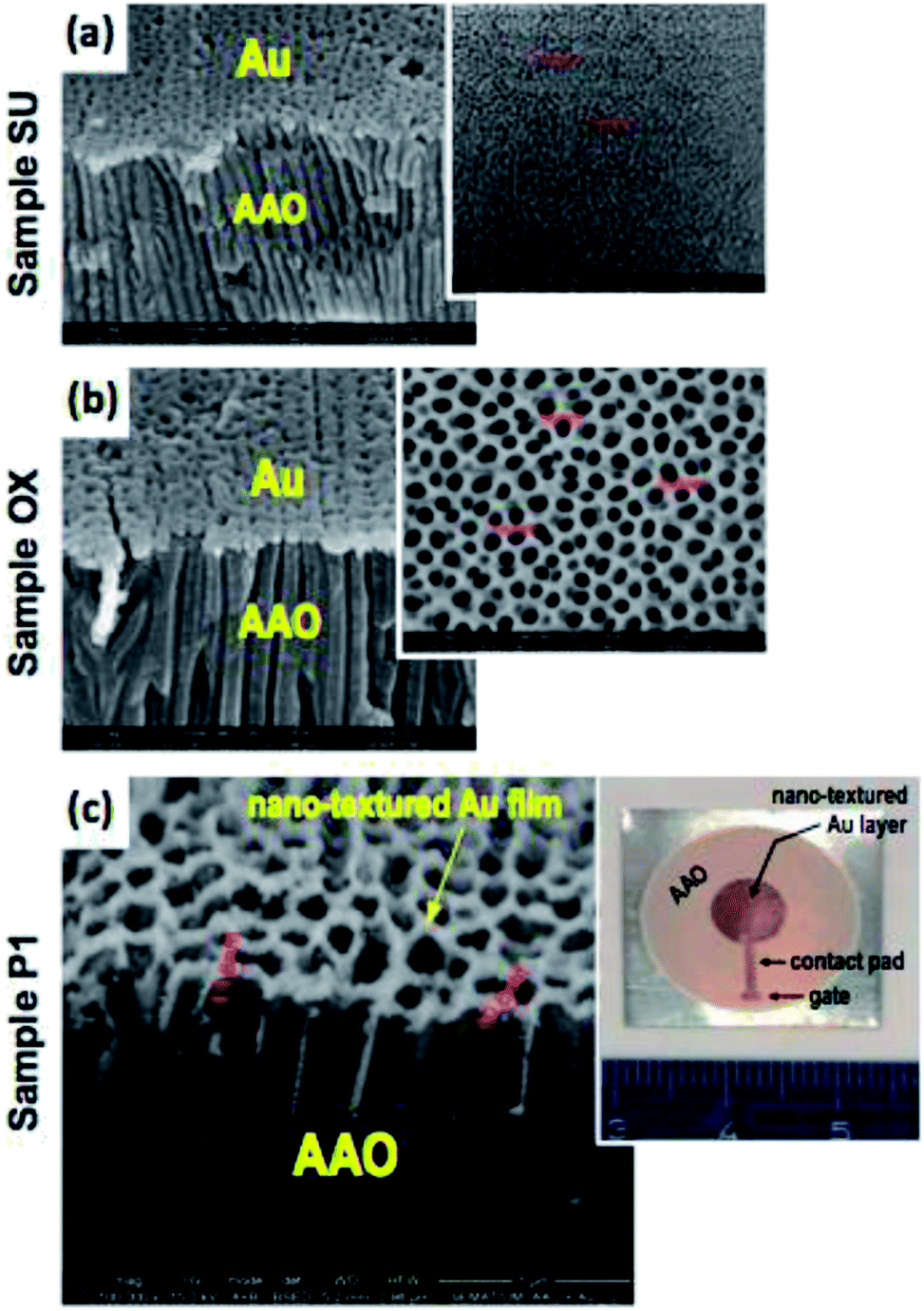 | ||
| Fig. 4 Side view SEM micrographs of nanotextured MIM (Au-AAO-Al) parallel-plate capacitor produced with (a) sulphuric acid electrolyte (sample SU); (b) oxalic acid electrolyte (sample OX) and (c) phosphoric acid electrolyte (sample P1). The insets shown in (a) and (b) correspond to the SEM top view micrographs of non-textured Au anodized samples SU and OX, respectively. The inset shown in (c) is a photo of the surface of sample P1 showing the general appearance of its nanotextured Au top electrode. | ||
Analysing SEM side view micrographs shown in Fig. 4(a–c) it can be concluded that, in general, for all the produced samples, the thermally evaporated gold was deposited homogeneously and mostly in the regions of the pore walls, thus making a nanoporous layer of Au on the surface of the AAO nanostructures. This evidence is attested by examining Fig. 4(c), which is the SEM micrograph of sample P1 acquired with backscattered electrons (BSE), therefore enabling to observe the typical atomic brightness contrast related with the existence of two different materials, namely alumina and gold. In addition, compared to AAO structures before the deposition of Au the average diameters of pores have been slightly reduced after the deposition of Au, which can influence the electrical response of these AAO structures. According to Nielsch et al.37 the porosity P (volume fraction of nanopores) of the AAO-based capacitive touch sensor can be expressed as,
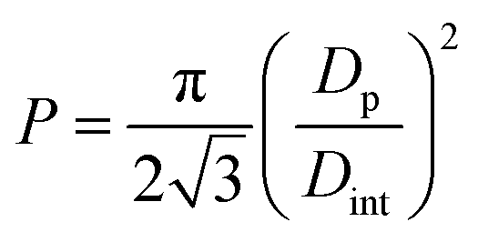 | (2) |
 | (3) |
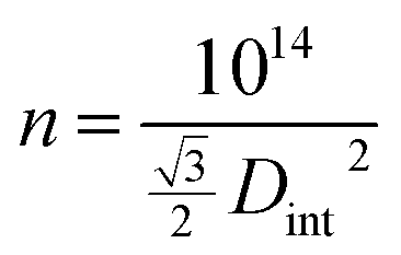
In order to evaluate AAO structural parameters, a statistical analysis was performed over the top view SEM micrographs presented in Fig. 3 and 4 by using the image-processing program, ImageJ. Table 2 show the structural dimensions for the produced AAO nanostructures.
| Sample ID | Pore diameter, Dp (nm) | Inter-pore distance, Dint (nm) | Calculated porosity, P (%) | Calculated pore density, n (pore/cm2) |
|---|---|---|---|---|
| SU | 21.8 | 45.2 | 21.0 | 5.6 × 10¹⁰ |
| OX | 58.0 | 118.7 | 22.0 | 8.1 × 10⁹ |
| P1 | 183.0 | 294.8 | 35.0 | 1.3 × 10⁹ |
Table 2 does not include results of the structural parameters for sample P2, since the morphology of this sample does not present self-organized pores due to the almost complete destruction of its nanoporous structure arising from the collapse of pore walls. For the other samples, the results shown in Table 2 reveal that the structural parameters of AAO samples are strongly dependent on the anodizing conditions (i.e. hard or mild conditions). For example, concerning the sample P1, fabricated with 0.3 M phosphoric acid electrolyte (U = 150 V and T = 0 °C), the values of its structural parameters, namely Dp, Dint and P are about 8.4, 6.5 and 1.6 times higher than those the obtained for sample SU. As a consequence, sample P1 has a pore density that is markedly smaller (about 43 times lower) than that of the SU sample.
4.2 Capacitive characteristics of the AAO capacitive sensor
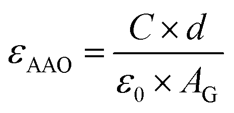
The capacitances of the fabricated AAO-based parallel-plate capacitors were estimated with the help of an LCR meter (QuadTech 1920 Precision LCR Meter), under a 100 kHz input signal with an amplitude of 1.0 V. This frequency was chosen because it is the one for which we obtained the lowest material dielectric losses (below 1%). The dielectric constant of the AAO material (εAAO) can be expressed as,
 | (4) |
Fig. 5 shows the capacitance variations, ΔC (from which the sensors' sensitivity was calculated) for AAO sensors as the Au top detection electrodes come into contact with a metal Al circular disk with 7.5 mm in diameter (inset).
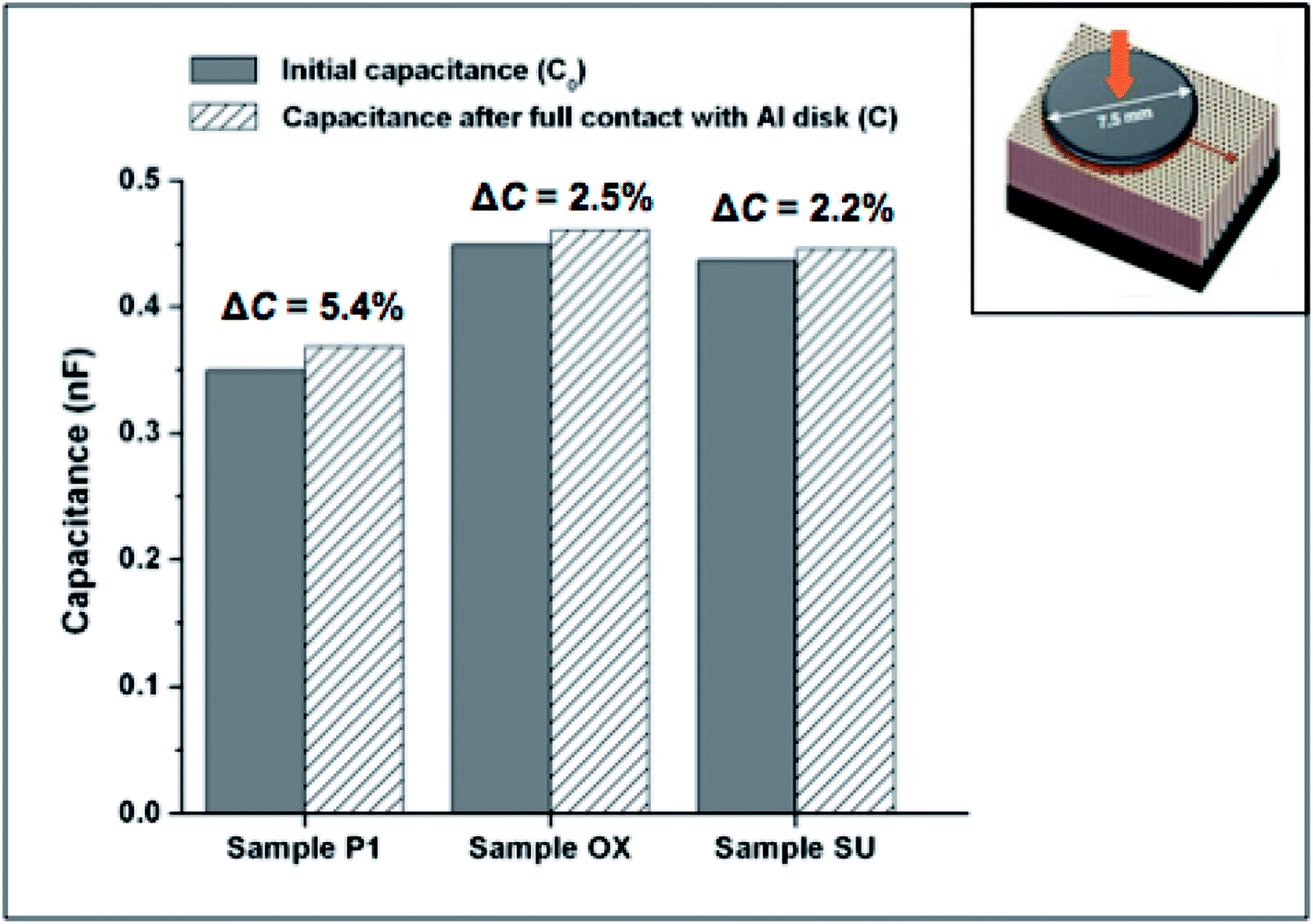 | ||
| Fig. 5 The initial measured capacitance and the capacitance after the full contact of an Al disk with the Au nanotextured top electrode of the AAO capacitive sensor. | ||
Noteworthy is that the initial capacitance is the capacitance of the AAO sensor with open pores but not covered by the metal Al circular disk. Thus, the greater the deviation of the capacitance from the AAO sensor initial capacitance, higher the device sensitivity is.
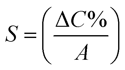
For example, considering the measured capacitance for sample P1 and applying eqn (4), the dielectric constant (εAAO) can be estimated to be 8.69, which is close to the values typically reported in literature.38,39 In this work, the sensitivity, S, of the AAO-based capacitive touch sensors in contact with the metal Al circular disk was determined using eqn (5)40
 | (5) |
In fact, as the Al circular disk makes contact with the nanotextured Au film, AAO nanopores (containing air inside) will be covered and as a consequence, a variation in the sensor capacitance, ΔCair, can be observed, as schematized in Fig. 1(c). If the surface of touch sensor is entirely covered by the Al disk (see Fig. 5), the theoretical change in the sensing area is A × P and the theoretical capacitance variation can be estimated as ΔCair = [ε0εair(A × P)/d], where εair is the dielectric constant of air. The sample P1 has the highest theoretical variation for sensor capacitance (ΔCair = 6.2%), which is a slightly higher value than the one experimentally obtained (ΔC = 5.4%), thus suggesting the highest capacitance variation, could be chosen to evaluate the performance of the AAO capacitive sensor for bacterial sensing applications.
4.3 Performance of the AAO sensor for bacterial sensing applications
For a biological application, the AAO sensor was used to detect the presence over time of E. coli through micro-touch type sensing tests. Fig. 6(a–c) shows the time variation of capacitance for the AAO touch sensor measured before (clean sensor) and after the contact with E. coli bacteria. On the other hand, Fig. 6(d) shows the variation with time of the capacitance for the control sensor (AC), which refers to the sample that was only immersed in the LB liquid medium (i.e. without the presence of E. coli). Triangular dotted lines used as reference in Fig. 6(a–c) denote the recorded signal from the clean sensor (i.e. with no bacterial suspension)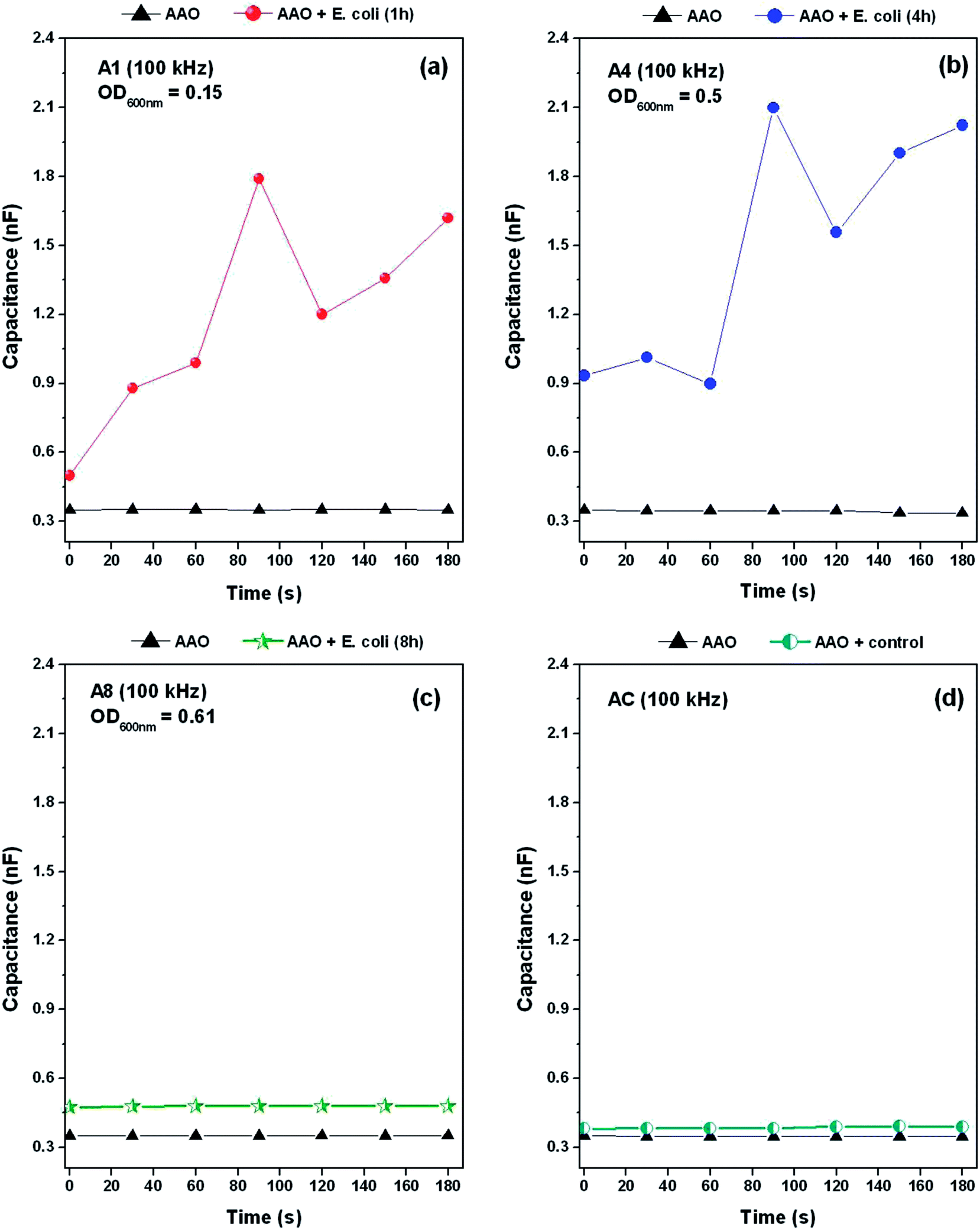 | ||
| Fig. 6 Measurement of the capacitance variation with time for the AAO touch sensor due to the contact with a suspension of Escherichia coli bacteria. The values were recorded from (a) sample A1 (E. coli grown for 1 h) (b) sample A4 (E. coli grown for 4 h) (c) sample A8 (E. coli grown for 8 h) and (d) control sample AC that does not contain E. coli as it was only immersed in the LB liquid medium. The triangular dots (identified as AAO) correspond to the recorded signal from the clean sensor (i.e. without liquid medium and E. coli), which is used as reference. | ||
It can be observed that the capacitance of sensors has experienced great intermittent variations during the time interval in which the capacitance measurements were taken for the samples A1 and A4 (see Fig. 6(a) and (b), respectively). It is also noticeable that, in general, there is a tendency to an increase in the value of capacitance over time. The aforementioned figures also present the measured optical density values of the culture medium, OD600 = 0.15 and OD600 = 0.50 for samples A1 and A4, respectively. The values clearly show that the suspension used for sample A4 hold a much higher amount of bacteria than that of sample A1. In addition, this condition is also expressed by the values recorded for the capacitance at t = 0 s, which are about 0.49 nF and 0.93 nF for sample A1 and A4, respectively.
In contrast, the sample A8, despite the existing amount of bacteria (OD600 = 0.61) is higher than that for the previous two samples, it is surprising that the recorded values for capacitance remain constant during the measurement period, showing an average ΔC% of about 35.7%, which result from the increase in the measured capacitance when compared with the clean sensor. Furthermore, still keeping the comparison with the clean sensor, the AC control sample shows no significant changes in capacitance during the measurement time, as would be already expected.
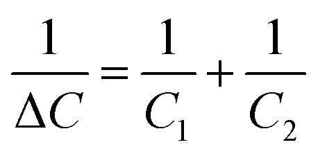
After the stipulated incubation period, the AAO sensors were subjected to a drying process in an oven at 40 °C for 1 h. Taking these experimental conditions and assuming a total evaporation of the LB liquid medium (the pores should only contain air inside), it is expected that E. coli has deposited on the nanotextured surface of the Au electrode, thus making the necessary electrical contact. Under these conditions, the AAO sensor's capacitance variation would result from the addition of new capacitors, connected in parallel, where the dielectric medium is air (εair = 1). In this case, the theoretical capacitance change is estimated as 6.2%, as already mentioned. However, this value is far from the ones experimentally recorded. This observation suggests that some volume of the LB culture medium possibly remains inside the pores of the AAO structures, which can occur because the surface position of bacteria (covering the pores of the AAO nanostructures) could have avoided the evaporation of the LB liquid culture medium from the porous channels of the AAO nanostructure, since the temperature of 40 °C as well as samples exposed for 1 h inside the oven correspond to very moderate conditions. Under this situation, each individual pore would act (in a simplified arrangement) as two capacitors in series, where the effective dielectric constant has a contribution from the LB culture medium as well, as schematically shown in Fig. 7.
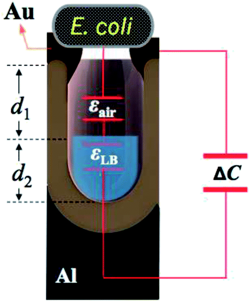 | ||
| Fig. 7 Schematic for a single pore of an AAO-based capacitive sensor, where the volume inside is partially filled by air while the rest is filled by the LB culture medium. The capacitance variation (ΔC) results from the series connection of two capacitors with different dielectric constants (εair and εLB) and thicknesses (d1and d2). | ||
The total effective capacitance variation, ΔC, can be determined as,
 | (6) |
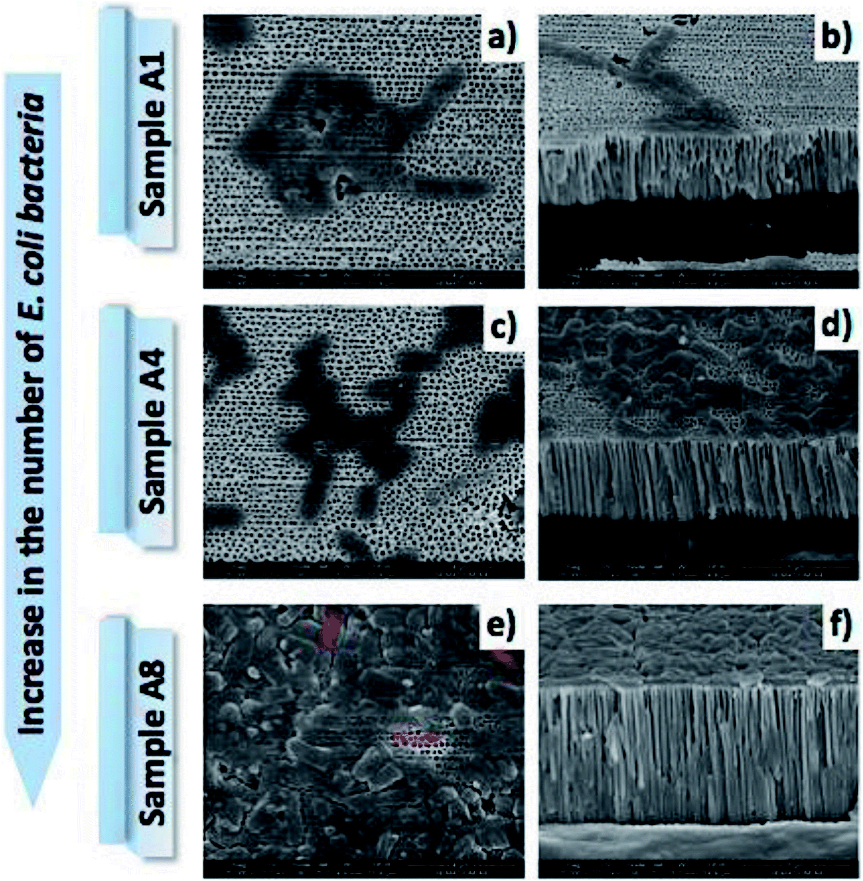 | ||
| Fig. 8 SEM micrographs showing the E. coli cells located on the surface of the nanotextured Au electrode (deposited by thermal evaporation onto the nanoporous AAO structures). Micrographs (a), (c) and (e) are top view, and (b), (d) and (f) are side view micrographs of AAO-based sensors A1, A4 and A8, respectively. | ||
For the case of A1 and A4 sensors, it is also possible to observe that the amount of bacteria was not sufficient to entirely cover the surface area of the Au electrode (see Fig. 8(a–d)). This finding confirms that the results shown in Fig. 6(a) and (b), revealing a very high increase in the capacitance of A1 and A4 samples, can not only be explained by the presence of bacteria on the surface of the Au electrode avoiding the evaporation of the LB liquid from the AAO nanoporous channels. It is anticipated that the moment the capacitance measurements were carried out, many bacteria would still be alive, presenting an adequate mobility to cause changes in the recorded capacitance. This assumption is justified because, as the population of the bacterial colony is relatively low (due to the moderately low incubation time for samples A1 and A4, respectively), as Semenov et al. reported,43 there could be a weak competition between them in order to consume the “food” that is provided by a certain volume of the LB culture medium still enclosed in the pores of the AAO structure. Although this is a not a widely investigated topic, there is strong evidence that living microorganisms that make up a bacterial colony holds specific communication mechanisms for their cooperation and survival in community.44 The work developed by Maxim44 proves that one of the communication mechanisms used by bacteria is associated with the emission of infrared radiation (IR). In this context, we speculate that there is the possibility that the IR radiation frequency, emitted by the bacteria resting on the surface of the AAO structures, may be capable of selectively exciting determined vibration eigenmodes (and/or to cause some localized temperature changes), thus contributing to significant changes in the electrical properties of the AAO material or its surroundings. Nevertheless, this speculation needs further scientific investigation.
5. Conclusions
Nanoporous anodic aluminium oxides were successfully produced from three different types of electrolytes, namely sulphuric acid, oxalic acid and phosphoric acid by using a cylindrical homemade anodization cell made from a solid polycarbonate billet via a lathe machining process. Depending on the anodizing conditions, different AAO morphologies (pore size, inter-pore distance and porosity) were achieved and it was demonstrated that they influence the sensitivity and performance of capacitive touch sensors based on the manufactured AAO structures. The experimental results show that the best capacitive response for the AAO-based capacitive touch sensor was attained by using specific anodizing conditions requiring the use of 0.3 M phosphoric acid at 150 V, 0 °C and a very fast anodizing process (∼40 s), because the initial capacitance for this Au-AAO-Al parallel-plate MIM capacitor (P1 sample) has been increased by 5.4% and its corresponding sensitivity was of 0.12 ΔC%/mm2. This is a much higher value than the ones recorded for the other two sensors, namely the OX sample and SU sample, which presented sensitivity values of 0.06 ΔC%/mm2 and 0.05 ΔC%/mm2, respectively.As a biological application, the AAO-based capacitive touch sensor has been successfully implemented to detect the presence and progress over time of a given amount of E. coli bacteria in contact with the Au nanotextured surface of the AAO-based sensor. It was found that depending on the amount of bacteria present on the Au nanotextured surface of the AAO-based sensor, its capacitive response also varied, indicating the occurrence of different interaction mechanisms between the culture of bacteria and the sensor.
Conflicts of interest
There are no conflicts to declare.Acknowledgements
This study was supported by the Portuguese Fundação para a Ciência e a Tecnologia (FCT) under the scope of the strategic funding of UID/FIS/04650/2013 and UID/BIO/04469/2013 units and COMPETE 2020 (POCI-01-0145-FEDER-006684). Artur Ribeiro thanks FCT for funding the scholarship with the reference SFRH/BPD/98388/2013.References
- H. Buff, Über das electrische Verhalten des Aluminiums, Liebigs Ann. Chem., 1857, 102(2006), 265–284 CrossRef.
- P. G. Sheasby and R. Pinner, The Surface Treatment and Finishing of Aluminium and Its Alloys, 6th edn, Finishing Publications Ltd. & ASM International, Materials Park, OH, and Stevenage, UK, 2001 Search PubMed.
- H. Masuda and K. Fukuda, Ordered Metal Nanohole Arrays Made by a Two Step Replication of Honeycomb Structures of Anodic Alumina, Science, 1995, 268(5216), 1466–1468 CrossRef CAS PubMed.
- H. Masuda and M. Satoh, Fabrication of Gold Nanodot Array Using Anodic Porous Alumina as an Evaporation Mask, Jpn. J. Appl. Phys., 1996, 35(Part 2, No. 1B), L126–L129 CrossRef CAS.
- D. H. Park, H. Seung Kim, M.-Y. Jeong, Y. Baek Lee, H.-J. Kim, D.-C. Kim, J. Kim and J. Jo, Significantly Enhanced Photoluminescence of Doped Polymer-Metal Hybrid Nanotubes, Adv. Funct. Mater., 2008, 18(17), 2526–2534 CrossRef CAS.
- Ki H. Young, D. Hyuk Park, S. Kyu Park, H. Song, D.-C. Kim, J. Kim, H. H. Young, O. Kyung Park, B. Cheol Lee and J. Joo, Tuning and Enhancing Photoluminescence of Light-Emitting Polymer Nanotubes through Electron-Beam Irradiation, Adv. Funct. Mater., 2009, 19(4), 567–572 CrossRef.
- Y. K. Hong, D. H. Park, S. Gi Jo, M. H. Koo, D. -C. Kim, J. Kim, J. -S. Kim, S. -Y. Jang and J. Joo, Fine Characteristics Tailoring of Organic and Inorganic Nanowires Using Focused Electron-Beam Irradiation, Angew. Chem., Int. Ed., 2011, 50(16), 3734–3738 CrossRef CAS PubMed.
- T.-C. Chan, Y.-M. Lin, H.-W. Tsai and Z. M. Wang, Chien-Neng Liao, Yu-Lun Chueh, Growth of large-scale nanotwinned Cu nanowire arrays from anodic aluminum oxide membrane by electrochemical deposition process: controllable nanotwin density and growth orientation with enhanced electrical endurance performance, Nanoscale, 2014, 6, 7332–7338 RSC.
- S. Ghosh, T. Maiyalagan and R. N. Basu, Nanostructured conducting polymers for energy applications: towards a sustainable platform, Nanoscale, 2016, 8, 6921–6947 RSC.
- U. Khan, M. Irfan, W. J. Li, N. Adeela, P. Liu, Q. T. Zhang and X. F. Han, Diameter-dependent multiferroic functionality in hybrid core/shell NWs, Nanoscale, 2016, 8, 14956–14964 RSC.
- H. Wang, T. Chang, X. Li, W. Zhang, Z. Hu and A. M. Jonas, Scaled down glass transition temperature in confined polymer nanofibers, Nanoscale, 2016, 8(32), 14950–14955 RSC.
- A. Khan Kasi, J. Khan Kasi, M. Hasan, N. Afzulpurkar, S. Pratontep, S. Porntheeraphat and P. Apirak, Fabrication of low cost anodic aluminum oxide (AAO) tubular membrane and their application for hemodialysis, Adv. Mater. Res., 2012, 550–553, 2040–2045 Search PubMed.
- A. Belwalkar, E. Grasing, W. Van Geertruyden, Z. Huang and W. Z. Misiolek, Effect of Processing Parameters on Pore Structure and Thickness of Anodic Aluminum Oxide (AAO) Tubular Membranes, J. Membr. Sci., 2008, 319(1–2), 192–198 CrossRef CAS PubMed.
- G. Gorokh, A. Mozalev, D. Solovei, V. Khatko, E. Llobet and X. Correig, Anodic formation of low-aspect-ratio porous alumina films for metal-oxide sensor application, Electrochim. Acta, 2006, 52(4), 1771–1780 CrossRef CAS.
- E. P. Briggs, A. R. Walpole, P. R. Wilshaw, M. Karlsson and E. Pålsgård, Formation of highly adherent nano-porous alumina on Ti-based substrates: a novel bone implant coating, J. Mater. Sci.: Mater. Med., 2004, 15(9), 1021–1029 CrossRef CAS PubMed.
- M. Darder, P. Aranda, M. Hernández-Vélez, E. Manova and E. Ruiz-Hitzky, Encapsulation of enzymes in alumina membrane of controlled pore size, Thin Solid Films, 2006, 495(1), 321–326 CrossRef CAS.
- D. Gong, V. Yadavalli, M. Paulose, M. Pishko and A. Craig, Grimes, Controlled Molecular Release Using Nanoporous Alumina Capsules. Therapeutic Micro and Nanotechnology, Biomed. Microdevices, 2003, 5, 75–80 CrossRef CAS.
- J. Chen, S. Wang, L. Ding, Y. Jiang and H. Wang, Performance of through-hole anodic aluminum oxide membrane as a separator for lithium-ion battery, J. Membr. Sci., 2014, 461, 22–27 CrossRef CAS.
- Y.-keon Ahn, J. Park, D. Shin, S. Cho, Si Y. Park, H. Kim, Y. Piao, J. Yoo and Y. S. Kim, Enhanced electrochemical capabilities of lithium ion batteries by structurally ideal AAO separator, J. Mater. Chem. A, 2015, 3, 10715–10719 RSC.
- Y. Gao, Y. Lin, J. Chen, Q. Lin, Y. Wu, W. Su, W. Wang and Z. Fan, Three-dimensional nanotube electrode arrays for hierarchical tubular structured high-performance pseudocapacitors, Nanoscale, 2016, 8, 13280–13287 RSC.
- A. P. Samantilleke, J. O. Carneiro, P. Alpuim, V. Teixeira and T. T. Thu Thuy, Nanoporous alumina templates: anodisation and mechanical characterisation, Nanotechnology, 2012, 4, 319–342 Search PubMed.
- W. Lee and S. J. Park, Porous anodic aluminum oxide: anodization and templated synthesis of functional nanostructures, Chem. Rev., 2014, 114(5), 7487–7556 CrossRef CAS PubMed.
- P. G. Sheasby and R. Pinner, The Surface Treatment and Finishing of Aluminum and Its Alloys, 6th edn, Finishing Publications Ltd. & ASM International, Materials Park, OH, and Stevenage, UK, 2001 Search PubMed.
- W. Lee, R. Ji, U. Gösele and K. Nielsch, Fast fabrication of long-range ordered porous alumina membranes by hard Anodization, Nat. Mater., 2006, 5, 741–747 CrossRef CAS PubMed.
- Y. Li, M. Zheng, L. Ma and W. Shen, Fabrication of highly ordered nanoporous alumina films by stable high-field anodization, Nanotechnology, 2006, 17, 5101–5105 CrossRef CAS.
- S. Ono, M. Saito and H. Asoh, Self-Ordering of Anodic Porous Alumina Induced by Local Current Concentration: Burning, Electrochem. Solid-State Lett., 2004, 7(7), B21–B24 CrossRef CAS.
- H. K. Lee, S. I. Chang and E. Yoon, A flexible polymer tactile sensor: Fabrication and modular expandability for large area deployment, J. Microelectromech. Syst., 2006, 15(6), 1681–1686 CAS.
- J. P. Bergstrom and T. Dong, Rapid Detection of E. coli Cells in Urine Samples using a Self-Capacitance Touchscreen Device, IEEE Engineering in Medicine and Biology Society Conference Proceedings, 2015, pp. 5545–5548 Search PubMed.
- C. Hong, L. Chu, W. Lai, A.-S. Chiang and W. Fang, Implementation of a New Capacitive Touch Sensor Using the Nanoporous Anodic Aluminum Oxide (np-AAO) Structure, IEEE Sens. J., 2011, 11(12), 3409–3415 CAS.
- N. Idil, M. Hedström, A. Denizli and B. Mattiasson, Whole cell based microcontact imprinted capacitive biosensor for the detection of Escherichia coli, Biosens. Bioelectron., 2017, 87, 807–815 CrossRef CAS PubMed.
- A. P. Samantilleke, J. O. Carneiro, S. Azevedo, T. Thuy and V. Teixeira, Electrochemical Anodizing, Structural and Mechanical Characterization of Nanoporous Alumina Templates, J. Nano Res., 2013, 25, 77–89 CAS.
- M. Mibus, C. Jensen, X. Hu, C. Knospe, M. L. Reed and G. Zangari, Dielectric breakdown and failure of anodic aluminum oxide films for electrowetting systems, J. Appl. Phys., 2013, 114(1), 014901 CrossRef.
- G. K. Singh, A. A. Golovin and I. S. Aranson, Formation of Self-organized Nanoscale Porous Structures in Anodic Aluminum Oxide, Phys. Rev. B: Condens. Matter Mater. Phys., 2006, 73, 205422 CrossRef.
- X. Zhao, S.-K. Seo, U.-J. Lee and K.-H. Lee, Controlled Electrochemical Dissolution of Anodic Aluminum Oxide for Preparation of Open-Through Pore Structures, J. Electrochem. Soc., 2007, 154(10), C553–C557 CrossRef CAS.
- F. C. Walsh, The Overall Rates of Electrode Reactions: Faraday's Laws of Electrolysis, Trans. Inst. Met. Finish., 1991, 69(4), 155–157 CrossRef CAS.
- J. S. L. Leach and P. Neufeld, Pore structure in anodic Al2O3 films, Corros. Sci., 1969, 9(6), 413–421 CrossRef CAS.
- K. Nielsch, J. Choi, K. Schwirn and B. Ralf, Wehrspohn, Ulrich Gösele, Self-ordering Regimes of Porous Alumina: The 10 Porosity Rule, Nano Lett., 2002, 2(7), 677–680 CrossRef CAS.
- P. Lo, C.-C. Lee, W. Fang, Implementation of electrostatically controlled Fabry–Perot interferometer using nanoporous anodic aluminum oxide layer, Transducers 2013, Barcelona, Spain, 16-20 June 2013, pp. 677–680 Search PubMed.
- J. I. Sohn, Y.-S. Kim, C. Nam, B. K. Cho and S. Tae-Yeon, Fabrication of high-density arrays of individually isolated nanocapacitors using anodic aluminum oxide templates and carbon nanotubes, Appl. Phys. Lett., 2005, 87(12), 123115 CrossRef.
- G. R. Suma, N. K. Subramanic, S. Sachhidananda and S. V. Satyanarayana, Siddaramaiah, Nanotechnology Enabled E.Coli Sensors: An Opto-Electronic Study, Mater. Today, 2017, 4, 11300–11304 CrossRef.
- C. G. Malmberg and A. A. Maryott, Dielectric Constant of Water from 0 C° to 1000 °C, J. Res. Natl. Bur. Stand., 1956, 56(1), 2641 Search PubMed.
- C. Ren, L. Zeng and M. M. Zhou, Preparation, Biochemical Analysis, and Structure Determination of the Bromodomain, an Acetyl-Lysine Binding Domain, Methods Enzymol., 2016, 573, 321–343 CAS.
- A. V. Semenov, A. H. C. van Bruggen, Leo van Overbeek, A. J. Termorshuizen and A. M. Semenov, Influence of temperature fluctuations on Escherichia coli O157:H7 and Salmonella enterica serovar Typhimurium in cow manure, FEMS Microbiol. Ecol., 2007, 60(3), 419–428 CrossRef CAS PubMed.
- V. T. Maxim, Light-mediated ‘‘conversation’’ among microorganisms, Microbiol. Res., 2004, 159, 1–10 CrossRef PubMed.
Footnote |
| † Electronic supplementary information (ESI) available. See DOI: 10.1039/c8ra07490a |
| This journal is © The Royal Society of Chemistry 2018 |