High performance fiber-shaped perovskite solar cells based on lead acetate precursor†
Hsienwei
Hu
a,
Bin
Dong
a,
Buxin
Chen
a,
Xue
Gao
a and
Dechun
Zou
 *ab
*ab
aBeijing National Laboratory for Molecular Sciences, Key Laboratory of Polymer Chemistry and Physics of Ministry of Education, Center for Soft Matter Science and Engineering, College of Chemistry and Molecular Engineering, Peking University, Beijing 100871, China. E-mail: dczou@pku.edu.cn; Fax: +86-10-6275-9799; Tel: +86-10-6275-9799
bBeijing Engineering Research Center for Active Matrix Display, Peking University, Beijing 100871, China
First published on 23rd October 2017
Abstract
Research on perovskite solar cells is currently at a high level of activity and many types of special solar architectures have been derived. The fiber-shaped perovskite solar cell (FPSC) is one very important type of these architectures, as it could be a potential power source of portable/wearable electronics. For the first time, we introduce lead acetate as the lead source to improve the perovskite film morphology on highly curved fiber substrates and then enhance the FPSC performance. A large grain size and uniform perovskite film could be obtained via a simple dip-coating process. The FPSCs achieved a PCE of 7.53% and VOC of 0.96 V under AM 1.5 illumination. This non-halide lead source could promote the development of efficient and large-sized devices with solid fiber solar cells.
Introduction
Perovskite solar cells have attracted wide attention, the devices have achieved a certified power conversion efficiency (PCE) of 22.1% for lab device,1 and some large-area perovskite solar cells have attained efficiency of 19.6% in recent years.2 Thus, this type of solar cell has significant potential for practical photovoltaics. Moreover, perovskite solar cells have a wide range of raw materials, are of low cost to fabricate, and are all-solution-processed functional films.3 These characteristics provide a strong foundation for device preparation on fibrous substrates.Attempts to develop portable/wearable electronics or e-textiles are in rapid development. Fiber-shaped devices, such as strain sensors,4 light emitting devices,5 memory devices,6 thermoelectric power generators,7 nanogenerator-driven devices,8 solar cells,9–11 supercapacitors,12 and batteries,13 have also been developed. Among these devices, fiber-shaped solar cells are photoelectric conversion devices that are one-dimensional and linear shaped in the macro scale. They can be woven with each other or other functional fibers. Fiber-shaped solar cells are potential power sources for portable and wearable electronics.14,15
A fiber-shaped perovskite solar cell (FPSC) based on carbon nanotubes as a top electrode was reported in 2014 with a PCE of 3.3%.16 Lee et al. improved the surface morphology of the perovskite film by anti-solvent engineering, and achieved a PCE of 3.85%.17 Zou et al. applied the dip-coating process to fabricate the functional layers and used a thin film of gold nanoparticles as the semitransparent top electrode. Given the layer-by-layer optimization, the fill factor greatly improved with a best device PCE of 5.35%.18 Peng et al. recently applied a three-step method by the cathodic deposition process to fabricate FPSCs, which was a little complex as a regulation process. The PCE of their device was 7.2%.19 In addition, a wide-noodle-shaped perovskite solar cell has also been reported, which had a PCE of 9.49% with a piece-shaped active area of 1 mm × 5 mm.20 Given that the device shape is unlike the universally recognized fiber shape, the classification of the wide-noodle-shaped perovskite solar cell still has to be determined. These studies show that the coverage and grain size of perovskite layers on curved surfaces are critical for the high PCE of FPSCs. At present, all the reported FPSCs utilize PbCl2 or PbI2 as the lead source. A different lead source for the perovskite precursor solution may improve the perovskite film morphology on highly curved surfaces and enhance the FPSC performance.
Among the non-halide lead sources, lead acetate is a promising lead source.21–24 The normal transition process of Pb(CH3COO)2 and CH3NH3I into perovskite is described by the following equation:25
| Pb(CH3COO)2 + CH3NH3I + DMF → (CH3NH3I)x–PbI2–(DMF)y + CH3NH2↑ + DMF↑ + CH3COOH↑ | (1) |
| (CH3NH3I)x–PbI2–(DMF)y → CH3NH3PbI3 + DMF↑ + CH3NH3I↑ | (2) |
The by-product can be removed easily in the thermal annealing process. Thus, the perovskite crystal growth kinetics are much faster than halide lead sources, thereby allowing the generation of large grain sizes and almost pinhole-free perovskite films. This approach contributes to minimizing the defects in the perovskite film that can suppress interface charge recombination. Thus, the perovskite solar cells based on Pb(CH3COO)2 obtain a higher open-circuit voltage (Voc) than that of PbI2 or PbCl2, which is an important advantage of lead acetate as a lead source.26 Recently, conventional planar heterojunction perovskite solar cells using lead acetate [Pb(CH3COO)2] have achieved 20.15% efficiency.27
Results and discussion
For the first time, Pb(CH3COO)2 was used as a lead source in efficient FPSCs in this study. The fast perovskite crystal growth process leads to uniform and large-sized grain perovskite films on the highly curved fiber substrate due to its excellent film-forming property. We obtained high VOC of 0.96 V and a PCE of 7.53%; both are the best values achieved so far for FPSC to the best of our knowledge.The typical device structure of FPSC (i.e., Ti/c-TiO2/meso-TiO2/perovskite/spiro-OMeTAD/Au)18 is as shown in Fig. 1a. The specific process of each layer is detailed in the experimental section. Briefly, the compact TiO2 layer was prepared in situ on a titanium wire through electric heating, which was followed by a half-automation coating process with TiO2 colloids to form a uniformly mesoporous layer. The CH3NH3PbI3 perovskite layer with lead acetate as the lead source and a spiro-OMeTAD hole-transport layer fabrication underwent the dip-coating process. The thin film of gold nanoparticles was employed as the top electrode. The cross-sectional scanning electron microscope (SEM) image of the FPSC is shown in Fig. 1b.
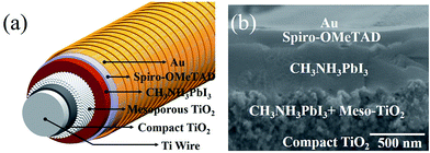 | ||
| Fig. 1 (a) Schematic and (b) cross-sectional SEM image of the FPSC based on the lead acetate precursor. | ||
The perovskite layer was dip-coated by the perovskite precursor solution, which was prepared by dissolving CH3NH3I and Pb(CH3COO)2 (molar ratio of 3![[thin space (1/6-em)]](https://www.rsc.org/images/entities/char_2009.gif) :
:![[thin space (1/6-em)]](https://www.rsc.org/images/entities/char_2009.gif) 1) in DMF with a 45 wt% concentration. We prepared the FPSCs with different annealing durations at 100 °C and compared the photovoltaic performance of the devices. When the annealing durations were increased from 5 min to 40 min, the PCE of the FPSCs also increased from 1.64% to 6.55% (Fig. 2a and Table S1†). When the annealing time was 10 min, the perovskite film exhibited many small-sized grains (Fig. 2b), and the FPSC obtained a VOC of 0.69 V and JSC of 4.47 mA cm−2. When the annealing time increased to 40 min, the perovskite materials exhibited a large grain size and almost full coverage of the film (Fig. 2c). The quality of the perovskite film was better than that of the perovskite films of the FPSCs based on PbCl2 or PbI2.16,18 However, if the annealing time increased to 60 min, it resulted in a lower surface coverage of perovskite films.28 An evident decrease in the short-circuit current density (Jsc) was also observed. The optimization of the annealing time in this work is 40 min, and the VOC and JSC of the FPSCs reached 0.89 V and 12.69 mA cm−2, respectively.
1) in DMF with a 45 wt% concentration. We prepared the FPSCs with different annealing durations at 100 °C and compared the photovoltaic performance of the devices. When the annealing durations were increased from 5 min to 40 min, the PCE of the FPSCs also increased from 1.64% to 6.55% (Fig. 2a and Table S1†). When the annealing time was 10 min, the perovskite film exhibited many small-sized grains (Fig. 2b), and the FPSC obtained a VOC of 0.69 V and JSC of 4.47 mA cm−2. When the annealing time increased to 40 min, the perovskite materials exhibited a large grain size and almost full coverage of the film (Fig. 2c). The quality of the perovskite film was better than that of the perovskite films of the FPSCs based on PbCl2 or PbI2.16,18 However, if the annealing time increased to 60 min, it resulted in a lower surface coverage of perovskite films.28 An evident decrease in the short-circuit current density (Jsc) was also observed. The optimization of the annealing time in this work is 40 min, and the VOC and JSC of the FPSCs reached 0.89 V and 12.69 mA cm−2, respectively.
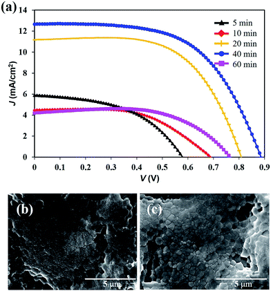 | ||
| Fig. 2 (a) J–V curves of the FPSCs with different annealing durations. Surface morphologies of the perovskite film with (b) 10 min and (c) 40 min annealing duration. | ||
Recent studies have revealed that water can positively affect the perovskite film, which can lead to better performance of the perovskite solar cell devices.29–31 We employed lead acetate trihydrate [Pb(CH3COO)2·3H2O] as the lead source in the hydration water introduction to improve the morphology of the perovskite film. This is because generating a uniform perovskite film on the curved substrate is difficult.
We regulated the equivalents of hydration water by varying the molar ratio between Pb (CH3COO)2 and Pb(CH3COO)2·3H2O in the perovskite precursor solution. For example, when the molar ratio between Pb(CH3COO)2 and Pb(CH3COO)2·3H2O is 1![[thin space (1/6-em)]](https://www.rsc.org/images/entities/char_2009.gif) :
:![[thin space (1/6-em)]](https://www.rsc.org/images/entities/char_2009.gif) 1, we apply Pb(CH3COO)2·1.5H2O to refer to the equivalents of hydration water. The effect of the different equivalents of hydration water in FPSCs was studied, and the results are summarized in Table 1.
1, we apply Pb(CH3COO)2·1.5H2O to refer to the equivalents of hydration water. The effect of the different equivalents of hydration water in FPSCs was studied, and the results are summarized in Table 1.
| Equivalents of hydration water | V OC (V) | J SC (mA cm−2) | FF | PCE (%) |
|---|---|---|---|---|
| 0 | 0.84 | 11.18 | 0.68 | 6.39 |
| 1.5 | 0.93 | 11.44 | 0.66 | 7.02 |
| 3 | 0.86 | 9.46 | 0.61 | 4.96 |
Table 1 shows that the PCE of the FPSCs improved when Pb(CH3COO)2·1.5H2O was used as the lead source as the VOC of the devices was shown to increase. However, if more hydration water is placed in the perovskite precursor solution, then it produced excessive water in the system and forms (CH3NH3)4PbI6·2H2O, which would irreversibly decompose to PbI2.32 Therefore, the PCE of the FPSCs with Pb(CH3COO)2·3H2O as the lead source decreased instead. Comparing the surface morphologies of the perovskite films by Pb(CH3COO)2·1.5H2O and Pb(CH3COO)2·3H2O, the latter was clearly damaged (Fig. 3a and b). We then compared the X-ray diffraction (XRD) patterns of perovskite films between Pb(CH3COO)2·1.5H2O and Pb(CH3COO)2 as the lead source (Fig. S1†). The main diffraction peaks were all the same, but only a small diffraction peak at 12.4°, that corresponds to the (001) lattice planes of PbI2, was observed. This condition is attributed to part of the perovskite material decomposition into trace PbI2.
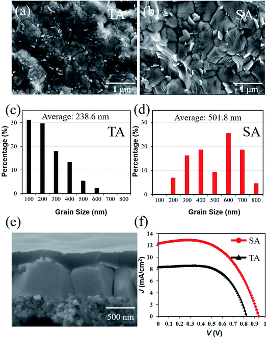
When using lead acetate as a lead source, the facile removal of by-product results in the fast crystallization of perovskite films. Thus, some small-sized grains with random crystal orientation are formed, which will inevitably increase the grain boundary density. Solvent annealing (SA) by DMF was conducted for grain growth, thereby improving the grain size of the perovskite material.33
On a fiber substrate, the perovskite grain size formed by the SA was also larger than that for thermal annealing (TA) only (Fig. 4a and b). The average grain sizes of the perovskite film increased from 238 nm (Fig. 4c) to 501 nm (Fig. 4d). After SA, the percentage of small-sized grains decreased significantly, and the surface morphology tended to be smooth (Fig. S2†). The increase in the perovskite grain size contributed to the lower grain boundary density, which can decrease the overall bulk defect density and trap states.34
The grains of the perovskite film by the SA process are also sufficiently large, wherein a single grain can connect the cathode and anode simultaneously (Fig. 4e). Related research shows that most of the charge carrier can reach the electrodes without encountering other grain boundaries, which can obviously lower the charge loss by recombination at the grain boundaries. The PCE of the FPSCs increased significantly by SA from 4.4% to 6.6% as shown in Fig. 4f. This is demonstrated by an improvement in the VOC and JSC of the devices. Given the obtained results, we consider SA to be a universal method, whose positive effect is unrestricted by the fiber-shaped substrate.
The length of a typical FPSCs is 4 cm in this work, which is the largest illumination area (0.25 mm × 40 mm = 10 mm2) among the reported FPSCs. A 4 cm FPSC exhibited a PCE of 5.51% (VOC of 0.96 V, JSC of 11.47 mA cm−2, and FF of 0.50). A VOC of 0.96 V is currently the highest value for FPSCs, which is almost consistent with the traditional flat perovskite solar cells. When the FPSC length was cut to 3 cm, the fill factor increased from 0.50 to 0.60, and the device PCE reached 6.43% (VOC of 0.94 V, JSC of 11.40 mA cm−2, and FF of 0.60) as shown in Fig. 5a. Increasing the FPSC length will cause the film defects to increase. Thus, the next step for large-sized FPSC devices is to develop a longer range and orderly approach to fabricating the functional layer on the fibrous substrate.
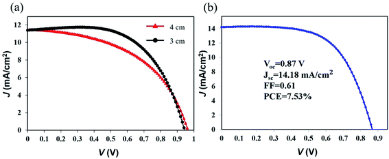 | ||
| Fig. 5 (a) J–V curves of the FPSCs with different device lengths. (b) J–V curve of the best-performing FPSC in this work. | ||
After integrating all of the optimizations for the perovskite layer, we obtained the best-performing FPSC, which achieved a PCE of 7.53% (Fig. 5b).
Conclusion
Lead acetate was introduced into the FPSC system as a lead source for the first time. The morphology and crystallization of the perovskite layer were improved by adjusting the thermal annealing time, different equivalents of hydration water, and SA processes. Large grain-sized and uniform perovskite films were obtained via a simple dip-coating process. We determined that the fast perovskite crystal growth kinetics by lead acetate can more easily form high-quality perovskite films on highly curved fiber substrates than traditional lead sources, such as PbI2 or PbCl2. The unique lead source materials present a new possibility of forming a high-quality perovskite film on unusual substrates. Finally, the maximum PCE and VOC of the FPSC achieved 7.53% and 0.96 V, respectively, which are the best reported values for solid fiber solar cells. This study will promote the development of efficient and large-sized devices of solid fiber solar cells. The research may also be further developed into wearable devices as power sources.Experimental section
Materials
The diameter of the Ti wire used was 250 μm (Alfa Aesar, 99.7%). Commercial TiO2 nanoparticle colloid (Dyesol DSL 18NR-T) was diluted with ethanol (1![[thin space (1/6-em)]](https://www.rsc.org/images/entities/char_2009.gif) :
:![[thin space (1/6-em)]](https://www.rsc.org/images/entities/char_2009.gif) 6.5 w/w) and then placed in an ultrasonic bath for 12 h. The Pb(CH3COO)2 was prepared from Pb(CH3COO)2·3H2O by vacuum drying at 75 °C for 6 h. The perovskite precursor solution was prepared by dissolving CH3NH3I and Pb(CH3COO)2 (molar ratio of 3
6.5 w/w) and then placed in an ultrasonic bath for 12 h. The Pb(CH3COO)2 was prepared from Pb(CH3COO)2·3H2O by vacuum drying at 75 °C for 6 h. The perovskite precursor solution was prepared by dissolving CH3NH3I and Pb(CH3COO)2 (molar ratio of 3![[thin space (1/6-em)]](https://www.rsc.org/images/entities/char_2009.gif) :
:![[thin space (1/6-em)]](https://www.rsc.org/images/entities/char_2009.gif) 1) in DMF with a concentration of 45 wt%. The spiro-OMeTAD solution was prepared by adding 72.3 mg of spiro-OMeTAD to 1 mL of chlorobenzene solution containing 28.8 μL of 4-tert-butyl pyridine and 17.5 μL of lithium bis(trifluoromethanesulfonyl)imide (Li-TFSI) solution (520 mg Li-TSFI in 1 mL acetonitrile, Sigma-Aldrich, 99.8%).
1) in DMF with a concentration of 45 wt%. The spiro-OMeTAD solution was prepared by adding 72.3 mg of spiro-OMeTAD to 1 mL of chlorobenzene solution containing 28.8 μL of 4-tert-butyl pyridine and 17.5 μL of lithium bis(trifluoromethanesulfonyl)imide (Li-TFSI) solution (520 mg Li-TSFI in 1 mL acetonitrile, Sigma-Aldrich, 99.8%).
Device fabrication
First, the Ti wires were pretreated by mechanical polishing and then cleaned sequentially using deionized water, acetone, and ethanol for 20 min in an ultrasonic bath. The compact TiO2 layer was prepared by electric heating in open air. The Ti wire was dip-coated using a half-automation coating setup with a dilute commercial TiO2 nanoparticle colloid solution then via electric heating to form the mesoporous TiO2 layer. The wire was dip-coated in the perovskite precursor solution followed by annealing at 100 °C for 40 min in nitrogen. After this the wire was covered by a glass Petri dish with 5 μL of DMF solvent, then solvent annealing at 100 °C for 10 min was performed. The as-prepared wire was dip-coated in spiro-OMeTAD solution to coat the hole transport layer. Finally, the thin gold electrode was prepared by magnetron sputtering, and a gold wire (diameter of 25 μm) entwined the FPSCs to adjunctively transfer the electric current. The details of the fabrication process can be found in Zou et al.18Measurement
The surface morphologies of the samples were observed using an SEM (S-4800 Hitachi, Japan).The grain size distributions of the SEM images were demarcated using Adobe Photoshop.
The XRD measurements were recorded with a Bruker diffractometer (D2 PHASER).
The part of the device without gold nanoparticles was scraped to expose the Ti wire as an anode. The part of FPSCs without gold wire entwining was cut off to confirm the illumination area. The J–V curves of the FPSCs were measured under AM 1.5 illumination (YDC-5A, Yamashita Denso, Japan). The fiber device was measured without any other substrate to avoid diffused light that led to the JSC deviation. The PCE of the FPSCs was calculated according to the method described in Peng and Zou.15
Conflicts of interest
There are no conflicts of interest to declare.Acknowledgements
This study is jointly supported by the National Natural Science Foundation of China (No. 51573004, No. 51773003, No. 51711540302), and the Beijing Natural Science Foundation (No. Z160002).References
- https://www.nrel.gov/pv/assets/images/efficiency_chart.jpg .
- X. Li, D. Bi, C. Yi, J. D. Decoppet, J. Luo, S. M. Zakeeruddin, A. Hagfeldt and M. Gratzel, A vacuum flash-assisted solution process for high-efficiency large-area perovskite solar cells, Science, 2016, 353(6294), 58–62 CrossRef CAS PubMed.
- M. Peng, W. Wen, S. Chen, B. Chen, K. Yan, H. Hu, B. Dong, X. Gao, X. Yu, X. Jiang and D. Zou, Organolead trihalide perovskite materials for efficient light emitting diodes, Sci. China: Chem., 2016, 59(6), 653–658 CrossRef CAS.
- J. Liu, W. Wu, S. Bai and Y. Qin, Synthesis of high crystallinity ZnO nanowire array on polymer substrate and flexible fiber-based sensor, ACS Appl. Mater. Interfaces, 2011, 3(11), 4197–4200 CAS.
- B. O'Connor, K. H. An, Y. Zhao, K. P. Pipe and M. Shtein, Fiber Shaped Light Emitting Device, Adv. Mater., 2007, 19(22), 3897–3900 CrossRef.
- K. Yan, B. Chen, H. Hu, S. Chen, B. Dong, X. Gao, X. Xiao, J. Zhou and D. Zou, First Fiber-Shaped Non-Volatile Memory Device Based on Hybrid Organic-Inorganic Perovskite, Adv. Electron. Mater., 2016, 2(8), 1600160 CrossRef.
- A. Yadav, K. P. Pipe and M. Shtein, Fiber-based flexible thermoelectric power generator, J. Power Sources, 2008, 175(2), 909–913 CrossRef CAS.
- Y. Qin, X. Wang and Z. L. Wang, Microfibre-nanowire hybrid structure for energy scavenging, Nature, 2008, 451(7180), 809–813 CrossRef CAS PubMed.
- X. Fan, Z. Z. Chu, F. Z. Wang, C. Zhang, L. Chen, Y. W. Tang and D. C. Zou, Wire-Shaped Flexible Dye-sensitized Solar Cells, Adv. Mater., 2008, 20(3), 592–595 CrossRef CAS.
- J. Liang, G. Zhang, Y. Yang and J. Zhang, Highly ordered hierarchical TiO2 nanotube arrays for flexible fiber-type dye-sensitized solar cells, J. Mater. Chem. A, 2014, 2(46), 19841–19847 CAS.
- Z. Zhang, Z. Yang, Z. Wu, G. Guan, S. Pan, Y. Zhang, H. Li, J. Deng, B. Sun and H. Peng, Weaving Efficient Polymer Solar Cell Wires into Flexible Power Textiles, Adv. Energy Mater., 2014, 4(11), 1301750 CrossRef.
- Y. Fu, X. Cai, H. Wu, Z. Lv, S. Hou, M. Peng, X. Yu and D. Zou, Fiber supercapacitors utilizing pen ink for flexible/wearable energy storage, Adv. Mater., 2012, 24(42), 5713–5718 CrossRef CAS PubMed.
- M. Peng, K. Yan, H. Hu, D. Shen, W. Song and D. Zou, Efficient fiber shaped zinc bromide batteries and dye sensitized solar cells for flexible power sources, J. Mater. Chem. C, 2015, 3(10), 2157–2165 RSC.
- D. Zou, D. Wang, Z. Chu, Z. Lv and X. Fan, Fiber-shaped flexible solar cells, Coord. Chem. Rev., 2010, 254(9–10), 1169–1178 CrossRef CAS.
- M. Peng and D. Zou, Flexible fiber/wire-shaped solar cells in progress: properties, materials, and designs, J. Mater. Chem. A, 2015, 3(41), 20435–20458 CAS.
- L. Qiu, J. Deng, X. Lu, Z. Yang and H. Peng, Integrating perovskite solar cells into a flexible fiber, Angew. Chem., Int. Ed. Engl., 2014, 53(39), 10425–10428 CrossRef CAS PubMed.
- M. Lee, Y. Ko and Y. Jun, Efficient fiber-shaped perovskite photovoltaics using silver nanowires as top electrode, J. Mater. Chem. A, 2015, 3(38), 19310–19313 CAS.
- H. Hu, K. Yan, M. Peng, X. Yu, S. Chen, B. Chen, B. Dong, X. Gao and D. Zou, Fiber-shaped perovskite solar cells with 5.3% efficiency, J. Mater. Chem. A, 2016, 4(10), 3901–3906 CAS.
- L. Qiu, S. He, J. Yang, J. Deng and H. Peng, Fiber-Shaped Perovskite Solar Cells with High Power Conversion Efficiency, Small, 2016, 12(18), 2419–2424 CrossRef CAS PubMed.
- L. Qiu, S. He, J. Yang, F. Jin, J. Deng, H. Sun, X. Cheng, G. Guan, X. Sun, H. Zhao and H. Peng, An all-solid-state fiber-type solar cell achieving 9.49% efficiency, J. Mater. Chem. A, 2016, 4(26), 10105–10109 CAS.
- J. Xu, A. Buin, A. H. Ip, W. Li, O. Voznyy, R. Comin, M. Yuan, S. Jeon, Z. Ning, J. J. McDowell, P. Kanjanaboos, J. P. Sun, X. Lan, L. N. Quan, D. H. Kim, I. G. Hill, P. Maksymovych and E. H. Sargent, Perovskite-fullerene hybrid materials suppress hysteresis in planar diodes, Nat. Commun., 2015, 6, 7081 CrossRef CAS PubMed.
- L. Zhao, D. Luo, J. Wu, Q. Hu, W. Zhang, K. Chen, T. Liu, Y. Liu, Y. Zhang, F. Liu, T. P. Russell, H. J. Snaith, R. Zhu and Q. Gong, High-Performance Inverted Planar Heterojunction Perovskite Solar Cells Based on Lead Acetate Precursor with Efficiency Exceeding 18%, Adv. Funct. Mater., 2016, 26(20), 3508–3514 CrossRef CAS.
- K. Chen, Q. Hu, T. Liu, L. Zhao, D. Luo, J. Wu, Y. Zhang, W. Zhang, F. Liu, T. P. Russell, R. Zhu and Q. Gong, Charge-Carrier Balance for Highly Efficient Inverted Planar Heterojunction Perovskite Solar Cells, Adv. Mater., 2016, 28(48), 10718–10724 CrossRef CAS PubMed.
- W. Zhang, S. Pathak, N. Sakai, T. Stergiopoulos, P. K. Nayak, N. K. Noel, A. A. Haghighirad, V. M. Burlakov, D. W. deQuilettes, A. Sadhanala, W. Li, L. Wang, D. S. Ginger, R. H. Friend and H. J. Snaith, Enhanced optoelectronic quality of perovskite thin films with hypophosphorous acid for planar heterojunction solar cells, Nat. Commun., 2015, 6, 10030 CrossRef CAS PubMed.
- Q. Hu, L. Zhao, J. Wu, K. Gao, D. Luo, Y. Jiang, Z. Zhang, C. Zhu, E. Schaible, A. Hexemer, C. Wang, Y. Liu, W. Zhang, M. Gratzel, F. Liu, T. P. Russell, R. Zhu and Q. Gong, In situ dynamic observations of perovskite crystallisation and microstructure evolution intermediated from [PbI6]4− cage nanoparticles, Nat. Commun., 2017, 8, 15688 CrossRef CAS PubMed.
- W. Zhang, M. Saliba, D. T. Moore, S. K. Pathak, M. T. Horantner, T. Stergiopoulos, S. D. Stranks, G. E. Eperon, J. A. Alexander-Webber, A. Abate, A. Sadhanala, S. Yao, Y. Chen, R. H. Friend, L. A. Estroff, U. Wiesner and H. J. Snaith, Ultrasmooth organic-inorganic perovskite thin-film formation and crystallization for efficient planar heterojunction solar cells, Nat. Commun., 2015, 6, 6142 CrossRef CAS PubMed.
- D. Luo, L. Zhao, J. Wu, Q. Hu, Y. Zhang, Z. Xu, Y. Liu, T. Liu, K. Chen, W. Yang, W. Zhang, R. Zhu and Q. Gong, Dual-Source Precursor Approach for Highly Efficient Inverted Planar Heterojunction Perovskite Solar Cells, Adv. Mater., 2017, 29(19), 1604758 CrossRef PubMed.
- A. Dualeh, N. Tétreault, T. Moehl, P. Gao, M. K. Nazeeruddin and M. Grätzel, Effect of Annealing Temperature on Film Morphology of Organic-Inorganic Hybrid Pervoskite Solid-State Solar Cells, Adv. Funct. Mater., 2014, 24(21), 3250–3258 CrossRef CAS.
- H. Zhou, Q. Chen, G. Li, S. Luo, T. B. Song, H. S. Duan, Z. Hong, J. You, Y. Liu and Y. Yang, Photovoltaics. Interface engineering of highly efficient perovskite solar cells, Science, 2014, 345(6196), 542–546 CrossRef CAS PubMed.
- L. Ling, S. Yuan, P. Wang, H. Zhang, L. Tu, J. Wang, Y. Zhan and L. Zheng, Precisely Controlled Hydration Water for Performance Improvement of Organic-Inorganic Perovskite Solar Cells, Adv. Funct. Mater., 2016, 26(28), 5028–5034 CrossRef CAS.
- Z. Song, A. Abate, S. C. Watthage, G. K. Liyanage, A. B. Phillips, U. Steiner, M. Graetzel and M. J. Heben, Perovskite Solar Cell Stability in Humid Air: Partially Reversible Phase Transitions in the PbI2-CH3NH3I-H2O System, Adv. Energy Mater., 2016, 6(19), 1600846 CrossRef.
- A. M. A. Leguy, Y. Hu, M. Campoy-Quiles, M. I. Alonso, O. J. Weber, P. Azarhoosh, M. van Schilfgaarde, M. T. Weller, T. Bein, J. Nelson, P. Docampo and P. R. F. Barnes, Reversible Hydration of CH3NH3PbI3 in Films, Single Crystals, and Solar Cells, Chem. Mater., 2015, 27(9), 3397–3407 CrossRef CAS.
- J. Qing, H.-T. Chandran, H.-T. Xue, Z.-Q. Guan, T.-L. Liu, S.-W. Tsang, M.-F. Lo and C.-S. Lee, Simple fabrication of perovskite solar cells using lead acetate as lead source at low temperature, Org. Electron., 2015, 27, 12–17 CrossRef CAS.
- Z. Xiao, Q. Dong, C. Bi, Y. Shao, Y. Yuan and J. Huang, Solvent annealing of perovskite-induced crystal growth for photovoltaic-device efficiency enhancement, Adv. Mater., 2014, 26(37), 6503–6509 CrossRef CAS PubMed.
Footnote |
| † Electronic supplementary information (ESI) available. See DOI: 10.1039/c7se00462a |
| This journal is © The Royal Society of Chemistry 2018 |

