Higher efficiency perovskite solar cells using E-mail: Au@SiO2 core–shell nanoparticles
P. S.
Chandrasekhar
 ab,
Ashish
Dubey
a,
Khan Mamun
Reza
a,
M. D. Nazmul
Hasan
a,
Behzad
Bahrami
a,
Vamsi K.
Komarala
b,
James D.
Hoefelmeyer
d,
Qingquan
He
a,
Fan
Wu
a,
Hui
Qiao
a,
Wen-Hua
Zhang
 *c and
Qiquan
Qiao
 *a
*a
aCenter for Advanced Photovoltaics, Department of Electrical Engineering and Computer Science, South Dakota State University, Brookings, SD 57007, USA. E-mail: Qiquan.Qiao@sdstate.edu; Tel: +1-605-688-6965 Tel: +1-605-688-4401
bCenter for Energy Studies, Indian Institute of Technology Delhi, New Delhi-110016, India. Fax: +91 11 2659 1251; Tel: +91 11 2659 1255
cSichuan Research Center of New Materials, Institute of Chemical Materials, China Academy of Engineering Physics, Chengdu, P. R. China. E-mail: whzhang@caep.cn
dDepartment of Chemistry, University of South Dakota, 414 E. Clark St., Vermillion, SD 57069, USA
First published on 16th July 2018
Abstract
In this work, we improved photovoltaic performance by about 27% in planar p-i-n perovskite solar cells (PSCs) using plasmonic Au@SiO2 core–shell nanoparticles (NPs). The devices have an architecture of ITO glass/PEDOT:PSS/perovskite(CH3NH3PbI3)/PCBM/Rhodamine/Ag. Four batches of devices were fabricated with different concentrations of Au@SiO2 NPs ranging from 0.4 to 1.6 wt% with an interval of 0.4 wt%. The Au@SiO2 NPs were integrated at the interface between the PEDOT:PSS layer and the active perovskite layer. At an optimized concentration of 1.2 wt% Au@SiO2 NPs, the PSCs achieved 25.1% of enhancement in photocurrent from 17.45 to 22.35 mA cm−2 and an improvement of 27.3% in power conversion efficiency (PCE) from 11.44 to 14.57%. This significant improvement in device performance is attributed to the localized surface plasmon resonance (LSPR) of Au@SiO2 NPs, which enhanced the light absorption in the active perovskite layer. The transient photocurrent and photovoltage measurements revealed that PSCs with Au@SiO2 NPs have a faster charge transport time and longer recombination lifetime than those without Au@SiO2 NPs. These results demonstrate that plasmonic metal nanoparticles substantially improved the efficiency of PSCs.
1. Introduction
Organic–inorganic hybrid metal halide (CH3NH3PbX3, X = Cl, Br and I) perovskite solar cells (PSCs) have attracted a great interest in the photovoltaic community due to their tremendous improvement in power conversion efficiency (PCE). The enhancement in PCE is due to the unique properties of the hybrid perovskite materials such as high absorption coefficients, long charge carrier diffusion lengths, low cost and simple fabrication procedures, which make these PSCs a widely studied solar cell technology.1–5 In 2009, Miyasaka et al. first reported perovskite (CH3NH3PbI3) solar cells with a PCE of 3.8%.6 Recently, PSCs with a PCE of about 22% were reported and they showed the potential to reach the PCE of crystalline silicon (Si) solar cells.7–9 In order to enhance the PCE and stability of PSCs, several strategies and fabrication techniques are employed for improving the crystallinity and electronic properties of perovskite thin films and charge transportation in the device.8,10–14To further enhance the efficiency of PSCs, one of the finest approaches is to employ plasmonic metal nanoparticles (NPs) in between device layers for improving optical absorption in perovskite thin films without causing any changes in the perovskite layer and the device structure. Under light illumination, metal NPs produce localized surface plasmon resonances (LSPRs). Thus the collective oscillations of surface electrons on metallic nanostructures with confined electromagnetic energy will improve the light absorption of the active medium surrounding metal NPs.15–17 This phenomenon has been well studied in polymer solar cells, DSSCs and in Si solar cells for achieving high photovoltaic performance.18–22 Jang et al. clearly addressed the plasmonic enhancement mechanisms in all photovoltaic devices ranging from conventional Si solar cells to DSSCs, organic solar cells and perovskite solar cells.23 Snaith et al. demonstrated the enhancement in photocurrent and PCE in meso-superstructured PSCs by incorporating Au@SiO2 NPs into the Al2O3 matrix. The origin of improvement in photocurrent and PCE was attributed to the reduced exciton binding energy rather than enhanced light absorption.24 In another study, Snaith and co-workers reported a significant enhancement in photocurrent and PCE by incorporating Ag@TiO2 NPs into the active layer of the device. They proposed a theoretical model in which highly polarizable metal NPs improve the optical path length by acting as antennas for increasing the reabsorption of emitted radiation.25 Sun and co-workers addressed a unique sandwich structure of TiOx/Au NPs/TiOx in PSCs and observed an improved charge carrier transportation by the assistance of plasmonic-mediated hot carrier injection at the metal–semiconductor Schottky junction.26 Recently, Park et al. reported an improvement in the photovoltaic performance of PSCs by embedding Au NPs into the Spiro-OMeTAD hole transport layer.27
Herein, we successfully incorporated different concentrations (0.4, 0.8, 1.2 and 1.6 wt%) of Au@SiO2 core–shell NPs at the interface between the PEDOT:PSS hole transport layer and the active perovskite (CH3NH3PbI3) layer. At an optimized concentration (1.2 wt%) of Au@SiO2 NPs, we obtained a significant improvement in photocurrent by 25.1% from 17.45 to 22.35 mA cm−2 and PCE by 27.3% from 11.44 to 14.57%. The improved photovoltaic performance is attributed to the increased light absorption and enhanced charge transportation across the interface between the perovskite layer and the hole transport layer.
2. Experimental section
2.1. Materials
Chloroauric acid (HAuCl4·3H2O, >99%), tetraethoxysilane (TEOS, >99%), ammonia (30 wt% NH3 in water) and lead iodide (PbI2, 99%) were obtained from Acros Organics. Poly(vinylpyrrolidone) with an average molar mass of 40 kg mol−1 (PVP – 40), anhydrous dimethyl sulphoxide (DMSO, 99.9%), γ-butyrolactone (99%), rhodamine, ethanol (EtOH) and acetone were purchased from Sigma-Aldrich. Methylammonium iodide (CH3NH3I) was purchased from DyeSol (Australia). PEDOT:PSS (Clevios™ PVP AI 4083) was obtained from Heraeus. PC60BM was purchased from Nano-C. All materials were used as received without any modification.2.2. Device fabrication
Indium-doped tin dioxide (ITO) coated glass substrates were cleaned sequentially with a detergent, deionized water, acetone and isopropyl alcohol for 30 min by an ultrasonication treatment and finally subjected to oxygen plasma treatment for 25 min. A PEDOT:PSS layer was deposited on cleaned ITO glass substrates by spin coating at a speed of 4500 rpm for 90 s, followed by annealing at 145 °C for 10 min. For the plasmonic PSCs, Au@SiO2 core–shell NPs dispersed in ethanol with different concentrations were spun on top of the PEDOT:PSS film with a spinning speed of 3000 rpm for 30 s, followed by annealing at 125 °C for 5 min. The plasmonic Au@SiO2 core–shell NPs were synthesized by a two-step method. Initially, Au NPs without the SiO2 shell were synthesized according to the standard sodium citrate reduction method, followed by preparation of a SiO2 shell over Au NPs using tetraethyl orthosilicate (TEOS) by dispersing Au NPs in a solution of ammonia in ethanol.28,29 The Au@SiO2 core–shell NPs deposited over PEDOT:PSS films were transferred to a nitrogen (N2) filled glove-box for depositing an active perovskite layer. The perovskite precursor solution was prepared by dissolving CH3NH3I (209 mg) and PbI2 (581 mg) in a mixed solvent of 3![[thin space (1/6-em)]](https://www.rsc.org/images/entities/char_2009.gif) :
:![[thin space (1/6-em)]](https://www.rsc.org/images/entities/char_2009.gif) 7 volume ratio of DMSO and γ-butyrolactone, which was kept at 70 °C with continuous stirring overnight. The freshly prepared perovskite precursor solution was spin coated using a two step method at a speed of 750 rpm for 20 s and 4500 rpm for 60 s. In the second step of spin coating, 160 μl of toluene was drop casted after 40 s, and followed by annealing at 90 °C for 10 min. Phenyl-C61-butyric acid methyl ester (PCBM, 20 mg ml−1 in chlorobenzene) was spin coated on perovskite films with a spinning speed of 2000 rpm for 40 s followed by annealing at 80 °C for 5 min. The rhodamine buffer layer (0.5 mg ml−1 in isopropyl alcohol) was spun with a speed of 4000 rpm for 40 s. Finally, the silver (Ag) electrode (∼80 nm) was evaporated under a high vacuum of 2 × 10⁻⁶ torr using a shadow mask with an active area of 0.16 cm2.
7 volume ratio of DMSO and γ-butyrolactone, which was kept at 70 °C with continuous stirring overnight. The freshly prepared perovskite precursor solution was spin coated using a two step method at a speed of 750 rpm for 20 s and 4500 rpm for 60 s. In the second step of spin coating, 160 μl of toluene was drop casted after 40 s, and followed by annealing at 90 °C for 10 min. Phenyl-C61-butyric acid methyl ester (PCBM, 20 mg ml−1 in chlorobenzene) was spin coated on perovskite films with a spinning speed of 2000 rpm for 40 s followed by annealing at 80 °C for 5 min. The rhodamine buffer layer (0.5 mg ml−1 in isopropyl alcohol) was spun with a speed of 4000 rpm for 40 s. Finally, the silver (Ag) electrode (∼80 nm) was evaporated under a high vacuum of 2 × 10⁻⁶ torr using a shadow mask with an active area of 0.16 cm2.
2.3. Characterization
The morphology of as synthesized Au@SiO2 core–shell NPs was analyzed using transmission electron microscopy (TEM, Tecnai G2). The absorption spectra of Au and Au@SiO2 core–shell NPs and perovskite films with Au@SiO2 core–shell NPs were characterized using a UV-visible-NIR spectrophotometer (Agilent, G1103A). Scanning electron microscopy (SEM, Hitachi-S-4300N) and atomic force microscopy (AFM, Agilent 5500) were employed to analyze the surface morphology of perovskite films with and without Au@SiO2 core–shell NPs. Current density–voltage (J–V) characteristics were measured using an Agilent 4155C semiconductor parameter analyzer under one sun illumination (AM 1.5G, 100 mW cm−2) with a xenon arc lamp (AM 1.5 filter, Newport). Prior to the measurements, a National Renewable Energy Laboratory (NREL) calibrated photodetector was used to calibrate the distance between the device and the xenon arc lamp to ensure the light intensity of one sun condition. Incident photon to current conversion efficiency (IPCE) measurements were conducted using a xenon arc lamp attached to a monochromator (Newport). Transient photocurrent and photovoltage measurements were carried out using a mixed signal oscilloscope (Agilent Technologies, MSO-X 4154A) attached with a nitrogen-dye laser.3. Results and discussion
The PSCs having a device architecture (ITO/PEDOT:PSS/CH3NH3PbI3/PCBM/Ag) are shown in Fig. 1. Au@SiO2 core–shell NPs are introduced at the interface of the PEDOT:PSS layer and the perovskite layer. The morphology of as-synthesized Au@SiO2 core–shell NPs is presented in Fig. 2a. It was observed that the Au core size is around 40 nm in diameter and coated with an approximately 2 nm thin SiO2 shell. Without the SiO2 shell, the bare Au NPs will act as recombination centers when in contact with the perovskite material. Therefore, to protect the Au NPs, a thin SiO2 shell was coated around the bare Au NPs. The absorption spectra of Au NPs with and without the SiO2 shell dispersed in ethanol are shown in Fig. 2b. The bare Au NPs showed a SPR peak at around 527 nm, and for the Au@SiO2, the SPR peak was observed at ∼535 nm. The slight red shift in the absorption spectrum for Au@SiO2 is attributed to a change in the local refractive index of the surrounding medium upon the addition of a thin SiO2 shell.30 It is very critical to protect the bare metallic NPs (Au/Ag) by coating with either a titania (TiO2) or silica (SiO2) shell to minimize the charge carrier recombination in the photoactive layer for photovoltaic applications.31,32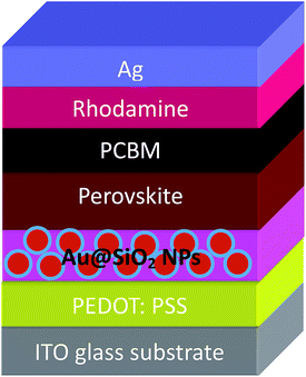 | ||
| Fig. 1 Schematic of a PSC architecture by incorporating Au@SiO2 NPs between PEDOT:PSS and the perovskite layer. | ||
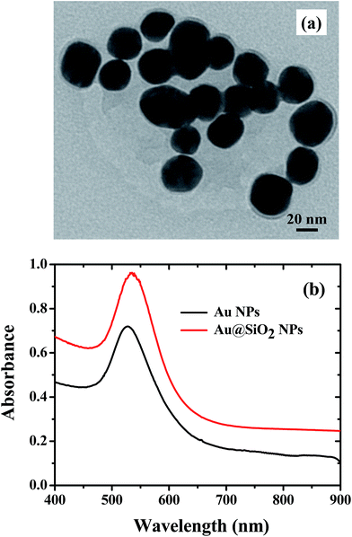 | ||
| Fig. 2 (a) TEM image of Au@SiO2 core–shell NPs. (b) Absorption spectra of Au NPs with and without a SiO2 shell in ethanol. | ||
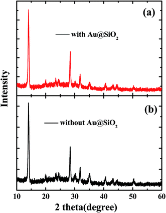
The SEM images of PEDOT:PSS films without and with Au@SiO2 NPs are presented in Fig. 3a and b. The surface morphologies of perovskite films coated on top of PEDOT:PSS without and with Au@SiO2 NPs are shown by SEM and AFM images in Fig. 3c–f, respectively. It was observed that the Au@SiO2 NPs are distributed over the PEDOT:PSS layer as shown in Fig. 3b (tiny white spots on the PEDOT:PSS film) and its corresponding perovskite film with Au@SiO2 NPs exhibited a well uniform and compact film without any pinholes (Fig. 3d) compared to the perovskite film without Au@SiO2 NPs (Fig. 3c). This is also supported by the AFM images (Fig. 3e and f). Thus, the perovskite film without Au@SiO2 NPs showed a slightly non-uniform morphology with a roughness of 13.8 nm and have narrow gaps (see red circles in Fig. 3e) and small grain boundaries among perovskite crystals. In comparison, the perovskite films with Au@SiO2 NPs show a decreased roughness (7.6 nm) and an absence of narrow gaps among perovskite crystals. Such an improvement in the morphology of perovskite films is attributed to the interfacial modification of the PEDOT:PSS film with Au@SiO2 NPs. To further study the difference in the morphology of perovskite films without and with Au@SiO2 NPs, we performed XRD measurements on perovskite films deposited on PEDOT:PSS films without and with Au@SiO2 NPs as shown in Fig. 4. In both cases, the perovskite films showed a similar diffraction pattern with nearly the same intensity. This clearly indicates that Au@SiO2 NPs do not influence the crystallinity of perovskite films. A similar observation was also reported by Wu et al. in PSCs via the integration of Au@SiO2 nanorods.33 However, in this work, we have observed a slight difference in the morphology and uniformity of perovskite films after adding Au@SiO2 NPs at the interface of PEDOT:PSS and the perovskite layer.
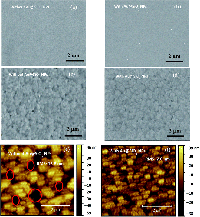 | ||
| Fig. 3 (a) and (b) SEM images of PEDOT:PSS films without and with Au@SiO2 core–shell NPs, and (c), (d), (e) and (f) SEM and AFM images of perovskite films without and with Au@SiO2 core–shell NPs. | ||
To investigate the role of Au@SiO2 NPs in photovoltaic performance, PSCs without and with different concentrations of Au@SiO2 NPs (0.4, 0.8, 1.2 and 1.6 wt%.) were fabricated. The J–V characteristics are presented in Fig. 5a and their photovoltaic parameters are summarized in Table 1. It was clearly observed that there is an enhancement in short-circuit density (JSC) and PCE, but a little change in the open-circuit voltage (VOC) and fill factor (FF). The control devices without Au@SiO2 NPs exhibited a JSC of 17.45 mA cm−2 and a PCE of 11.44%. The PSC device with an optimized concentration (1.2 wt%) of Au@SiO2 NPs showed an improvement in JSC by 25.1% from 17.45 to 22.35 mA cm−2 and PCE by 27.3% from 11.44 to 14.57%. This is a significant advancement over a recently reported JSC (20.04 mA cm−2) and PCE (12.74%) by employing bare Au NPs in the Spiro-OMeTAD hole transport layer solution.27 The reliability data are also included in Fig. 6 to ensure the improved photovoltaic performance of PSCs as a function of Au@SiO2 NPs having different concentrations. In our case, the improvement in JSC and PCE is attributed to the insertion of Au@SiO2 core–shell NPs between the PEDOT:PSS film and the perovskite film, which could efficiently trap the incident light and enhance the local electric field in the perovskite film. It is beneficial for improving the photovoltaic performance of PSCs by increasing light absorption in the device.18,34 Hsu et al. reported an improvement of JSC and PCE in organic solar cells and PSCs by integrating plasmonic Ag NPs with different sizes and shapes. The enhanced performance was attributed to the ability of plasmonic NPs to capture the light and increase the plasmonic scattering effect.35 Qian et al. embedded plasmonic Ag NPs resonating at ∼427 nm in PEDOT:PSS for mixed halide PSCs and reported than an enhancement in JSC and PCE is attributed to the improved hole extraction through the embedment of Ag NPs.36 Snaith et al. also demonstrated the plasmonic improvement in the performance of PSCs by mixing Au@SiO2 NPs into mesoporous Al2O3. The presence of SPR of Au NPs decreased the exciton binding energy within the perovskite material and resulted in a higher internal efficiency.24 Recently, Long et al. reported the plasmonic improvement of PSC performance from a nanostructured Au electrode, which enhanced the light absorption and increased the optical path length of the active perovskite layer.37 The above results and reports suggested that an improvement in the photovoltaic performance of PSCs is attributed to the SPR increased optical absorption of plasmonic metal NPs.
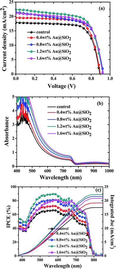 | ||
| Fig. 5 (a), (b) and (c) J–V characteristics, UV-visible absorption spectra and IPCE spectra of PSCs without and with Au@SiO2 core–shell NPs at different concentrations. | ||
| Device | V oc (V) | J sc (mA cm−2) | FF (%) | PCE (%) |
|---|---|---|---|---|
| Control | 0.89 ± 0.02 | 17.45 ± 0.21 | 71.69 ± 0.25 | 11.44 ± 0.11 |
| 0.4 wt% Au@SiO2 | 0.90 ± 0.01 | 19.57 ± 0.18 | 70.86 ± 0.19 | 12.48 ± 0.08 |
| 0.8 wt% Au@SiO2 | 0.93 ± 0.01 | 21.56 ± 0.13 | 68.85 ± 0.21 | 13.80 ± 0.23 |
| 1.2 wt% Au@SiO2 | 0.92 ± 0.02 | 22.35 ± 0.16 | 69.92 ± 0.28 | 14.57 ± 0.15 |
| 1.6 wt% Au@SiO2 | 0.92 ± 0.02 | 21.13 ± 0.19 | 67.59 ± 0.24 | 13.14 ± 0.21 |
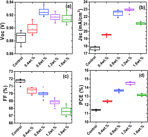 | ||
| Fig. 6 Photovoltaic parameters (a) Voc, (b) Jsc, (c) FF, and (d) PCE of PSCs as a function of different concentrations of Au@SiO2 NPs. *For each concentration twelve devices were fabricated. | ||
To further confirm the improvement of JSC and PCE, UV-visible absorption and IPCE measurements were also carried out and their corresponding spectra are presented in Fig. 5b and c, respectively. Fig. 5b shows a linear enhancement in the absorption of perovskite films with increasing concentration of Au@SiO2 NPs. It was demonstrated that Au@SiO2 NPs act as subwavelength antennas to couple incident light into the perovskite film, thereby improving the light absorption in the perovskite film. An improved near field electric effect is also responsible for increasing optical absorption.15 Therefore, an enhancement of PCE and JSC was obtained. These results were consistent with the IPCE spectral response (Fig. 5c). Fig. 5c confirms that the photon to current conversion is improved with increasing concentration of Au@SiO2 NPs. The integrated JSC is also calculated from the IPCE curves and is in good agreement with the Jsc values obtained from J–V curves. A significant enhancement in IPCE was obtained over almost the entire wavelength range (∼350 to ∼780 nm). In particular, the spectral response is highly improved in the range of ∼400 to ∼600 nm with increasing concentration of Au@SiO2 NPs. This is attributed to the plasmonic effect of Au@SiO2 NPs, which was caused by SPR absorption resonating at ∼535 nm. In addition to the plasmonic effect, improved electrical properties could also contribute to an improvement in JSC, PCE and spectral responses.33,38 Lee et al. reported that charge carrier recombination resistance was increased by integrating plasmonic Au NPs in PSCs. This showed that the Au NPs not only improved the optical absorption but also enhanced the electrical properties of the device, therefore leading to a higher JSC and PCE in devices.27 In another study, it was found that the series resistance of PSCs with plasmonic metal NPs is lower than that of PSCs without plasmonic metal NPs. A higher shunt resistance and larger recombination resistance were also observed for PSCs with plasmonic metal NPs than those without metal NPs.31 Thus, the improved electrical properties such as increased charge transport and decreased charge recombination could also be responsible for obtaining high JSC and PCE apart from an enhanced optical absorption.
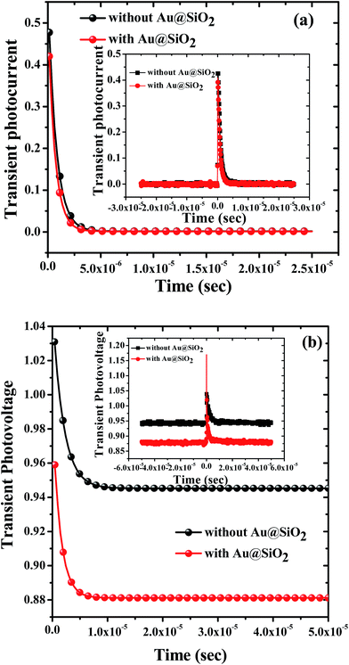
To understand the charge carrier dynamics, transient photocurrent (TPC) and transient photovoltage (TPV) decay measurements were performed to find out the charge transport time and charge carrier lifetime. Fig. 7a and b show mono-exponentially fitted decay and the corresponding raw data (insets) curves to calculate the charge transport time and lifetime for the devices prepared with 1.2 wt% and without Au@SiO2 NPs. Table 2 shows charge transport time and lifetime values for devices prepared with and without Au@SiO2. To obtain an enhanced charge collection, a faster (shorter) charge transport time and slower (longer) charge lifetime are desirable. It was observed that devices with Au@SiO2 showed a shorter charge transport time (0.665 μs) and a longer lifetime (1.95 μs) as compared to devices made without Au@SiO2 which showed a charge transport time of 0.782 μs and a lifetime of 1.40 μs. A short charge transport time and long lifetime will lead to an enhancement of charge collection in devices, resulting in higher device performance. The charge transport time and lifetime values obtained from TPC and TPV curves are in good agreement with the higher Jsc and Voc of devices prepared with and without Au@SiO2 NPs.
| Device | Charge transport time | Charge carrier life time |
|---|---|---|
| Without Au@SiO2 | 0.782 × 10⁻⁶ | 1.40 × 10⁻⁶ |
| With Au@SiO2 | 0.665 × 10⁻⁶ | 1.95 × 10⁻⁶ |
4. Conclusions
In summary, we have demonstrated plasmonic effects of Au@SiO2 core–shell NPs on the photovoltaic performance of planar heterojunction perovskite solar cells having an architecture of ITO/PEDOT:PSS/CH3NH3PbI3/PCBM/Rhodamine/Ag. Different concentrations of Au@SiO2 NPs were introduced at the interface of the PEDOT:PSS layer and perovskite layer. At an optimized concentration of Au@SiO2 NPs, we achieved a significant improvement in JSC by 25.1% from 17.45 to 22.35 mA cm−2 and PCE by 27.3% from 11.44 to 14.57%. The enhancement of device performance was attributed to an improved light trapping in the perovskite films by LSPR of Au@SiO2 NPs and the spectral response was also improved, especially in the range of 400 to 600 nm, because of Au@SiO2 NP's LSPR absorption resonating at around 535 nm. In addition, Au@SiO2 NPs provided a shorter charge transport time and a longer charge lifetime. This improved charge extraction and charge collection, resulting in an enhancement in JSC and PCE. Therefore, plasmonic metal NPs play a vital role in improving the photovoltaic performance of solar cells by enhancing light trapping and minimizing charge carrier recombination. The incorporation of plasmonic nanostructures has been demonstrated as one of the finest methods to enhance the JSC and PCE of solar cells.Conflicts of interest
The authors declare no conflict of interest.Acknowledgements
P. S. Chandrasekhar would like to thank the Indo-US science and technology forum (IUSSTF) for providing an internship through the Bhaskara Advanced Solar Energy Fellowship (BASE) program at South Dakota State University (SDSU), USA and is thankful to the Department of Science and Technology (DST), Govt. Of India for offering a fellowship under the DST-INSPIRE fellowship program (IF-120755). This work was also partly supported by NSF MRI, NASA EPSCoR, US-Egypt Joint Science and Technology, and the Pakistan–US Science and Technology Cooperation Program.References
- L. Etgar, P. Gao, Z. Xue, Q. Peng, A. K. Chandiran, B. Liu, M. K. Nazeeruddin and M. Grätzel, J. Am. Chem. Soc., 2012, 134, 17396–17399 CrossRef PubMed.
- J. Burschka, N. Pellet, S.-J. Moon, R. Humphry-Baker, P. Gao, M. K. Nazeeruddin and M. Gratzel, Nature, 2013, 499, 316–319 CrossRef PubMed.
- M. A. Green, K. Emery, Y. Hishikawa, W. Warta and E. D. Dunlop, Prog. Photovolt: Res. Appl., 2015, 23, 1–9 CrossRef.
- H. J. Snaith, J. Phys. Chem. Lett., 2013, 4, 3623–3630 CrossRef.
- H.-S. Kim, C.-R. Lee, J.-H. Im, K.-B. Lee, T. Moehl, A. Marchioro, S.-J. Moon, R. Humphry-Baker, J.-H. Yum, J. E. Moser, M. Grätzel and N.-G. Park, Sci. Rep., 2012, 2, 591 CrossRef PubMed.
- A. Kojima, K. Teshima, Y. Shirai and T. Miyasaka, J. Am. Chem. Soc., 2009, 131, 6050–6051 CrossRef PubMed.
- H. Zhou, Q. Chen, G. Li, S. Luo, T.-b. Song, H.-S. Duan, Z. Hong, J. You, Y. Liu and Y. Yang, Science, 2014, 345, 542–546 CrossRef PubMed.
- W. S. Yang, J. H. Noh, N. J. Jeon, Y. C. Kim, S. Ryu, J. Seo and S. I. Seok, Science, 2015, 348, 1234–1237 CrossRef PubMed.
- https://www.nrel.gov/pv/ .
- M. Liu, M. B. Johnston and H. J. Snaith, Nature, 2013, 501, 395–398 CrossRef PubMed.
- A. Mei, X. Li, L. Liu, Z. Ku, T. Liu, Y. Rong, M. Xu, M. Hu, J. Chen, Y. Yang, M. Grätzel and H. Han, Science, 2014, 345, 295–298 CrossRef PubMed.
- P. You, Z. Liu, Q. Tai, S. Liu and F. Yan, Adv. Mater., 2015, 27, 3632–3638 CrossRef PubMed.
- S. Das, B. Yang, G. Gu, P. C. Joshi, I. N. Ivanov, C. M. Rouleau, T. Aytug, D. B. Geohegan and K. Xiao, ACS Photonics, 2015, 2, 680–686 CrossRef.
- P. S. Chandrasekhar, N. Kumar, S. K. Swami, V. Dutta and V. K. Komarala, Nanoscale, 2016, 8, 6792–6800 RSC.
- H. A. Atwater and A. Polman, Nat. Mater., 2010, 9, 205–213 CrossRef PubMed.
- H. Chen, L. Shao, Q. Li and J. Wang, Chem. Soc. Rev., 2013, 42, 2679–2724 RSC.
- D. M. Schaadt, B. Feng and E. T. Yu, Appl. Phys. Lett., 2005, 86, 063106 CrossRef.
- L. Lu, Z. Luo, T. Xu and L. Yu, Nano Lett., 2013, 13, 59–64 CrossRef PubMed.
- S.-W. Baek, J. Noh, C.-H. Lee, B. Kim, M.-K. Seo and J.-Y. Lee, Sci. Rep., 2013, 3, 1726 CrossRef.
- K. Kim and D. L. Carroll, Appl. Phys. Lett., 2005, 87, 203113 CrossRef.
- J. Qi, X. Dang, P. T. Hammond and A. M. Belcher, ACS Nano, 2011, 5, 7108–7116 CrossRef PubMed.
- P. Spinelli, V. E. Ferry, J. v. d. Groep, M. v. Lare, M. A. Verschuuren, R. E. I. Schropp, H. A. Atwater and A. Polman, J. Opt., 2012, 14, 024002 CrossRef.
- Y. H. Jang, Y. J. Jang, S. Kim, L. N. Quan, K. Chung and D. H. Kim, Chem. Rev., 2016, 116, 14982–15034 CrossRef PubMed.
- W. Zhang, M. Saliba, S. D. Stranks, Y. Sun, X. Shi, U. Wiesner and H. J. Snaith, Nano Lett., 2013, 13, 4505–4510 CrossRef PubMed.
- M. Saliba, W. Zhang, V. M. Burlakov, S. D. Stranks, Y. Sun, J. M. Ball, M. B. Johnston, A. Goriely, U. Wiesner and H. J. Snaith, Adv. Funct. Mater., 2015, 25, 5038–5046 CrossRef.
- Z. Yuan, Z. Wu, S. Bai, Z. Xia, W. Xu, T. Song, H. Wu, L. Xu, J. Si, Y. Jin and B. Sun, Adv. Energy Mater., 2015, 5, 1500038 CrossRef.
- D. S. Lee, W. Kim, B. G. Cha, J. Kwon, S. J. Kim, M. Kim, J. Kim, D. H. Wang and J. H. Park, ACS Appl. Mater. Interfaces, 2016, 8, 449–454 CrossRef PubMed.
- C. Graf, D. L. J. Vossen, A. Imhof and A. van Blaaderen, Langmuir, 2003, 19, 6693–6700 CrossRef.
- B. V. Enustun and J. Turkevich, J. Am. Chem. Soc., 1963, 85, 3317–3328 CrossRef.
- J. Rodríguez-Fernández, I. Pastoriza-Santos, J. Pérez-Juste, F. J. García de Abajo and L. M. Liz-Marzán, J. Phys. Chem. C, 2007, 111, 13361–13366 CrossRef.
- M. D. Brown, T. Suteewong, R. S. S. Kumar, V. D'Innocenzo, A. Petrozza, M. M. Lee, U. Wiesner and H. J. Snaith, Nano Lett., 2011, 11, 438–445 CrossRef PubMed.
- S. W. Sheehan, H. Noh, G. W. Brudvig, H. Cao and C. A. Schmuttenmaer, J. Phys. Chem. C, 2013, 117, 927–934 CrossRef.
- R. Wu, B. Yang, C. Zhang, Y. Huang, Y. Cui, P. Liu, C. Zhou, Y. Hao, Y. Gao and J. Yang, J. Phys. Chem. C, 2016, 120, 6996–7004 CrossRef.
- Z. Lu, X. Pan, Y. Ma, Y. Li, L. Zheng, D. Zhang, Q. Xu, Z. Chen, S. Wang, B. Qu, F. Liu, Y. Huang, L. Xiao and Q. Gong, RSC Adv., 2015, 5, 11175–11179 RSC.
- H.-L. Hsu, T.-Y. Juang, C.-P. Chen, C.-M. Hsieh, C.-C. Yang, C.-L. Huang and R.-J. Jeng, Sol. Energy Mater. Sol. Cells, 2015, 140, 224–231 CrossRef.
- M. Qian, M. Li, X.-B. Shi, H. Ma, Z.-K. Wang and L.-S. Liao, J. Mater. Chem. A, 2015, 3, 13533–13539 RSC.
- M. Long, Z. Chen, T. Zhang, Y. Xiao, X. Zeng, J. Chen, K. Yan and J. Xu, Nanoscale, 2016, 8, 6290–6299 RSC.
- C. C. D. Wang, W. C. H. Choy, C. Duan, D. D. S. Fung, W. E. I. Sha, F.-X. Xie, F. Huang and Y. Cao, J. Mater. Chem., 2012, 22, 1206–1211 RSC.
| This journal is © The Royal Society of Chemistry 2018 |

