Design of cyclopentadithiophene-based small organic molecules as hole selective layers for perovskite solar cells†
Laura
Caliò
a,
Samrana
Kazim
ab,
Manuel
Salado
ab,
Iwan
Zimmermann
d,
Mohammad Khaja
Nazeeruddin
 d and
Shahzada
Ahmad
 *abc
*abc
aAbengoa Research, Abengoa, C/ Energía Solar no 1, Campus Palmas Altas-41014, Sevilla, Spain
bBCMaterials, Basque Center for Materials, Applications and Nanostructures, Bld. Martina Casiano, UPV/EHU Science Park, Barrio Sarriena s/n, 48940 Leioa, Spain. E-mail: shahzada.ahmad@bcmaterials.net; Tel: +34 946128811
cIKERBASQUE, Basque Foundation for Science, Bilbao, 48013, Spain
dGroup for Molecular Engineering of Functional Materials, Swiss Federal Institute of Technology Lausanne, EPFL Valais Wallis, CH-1951 Sion, Switzerland
First published on 11th May 2018
Abstract
Thiophene-based p-type molecules are being extensively investigated and employed in optoelectronic devices due to their intriguing semiconducting properties. Herein, we report the synthesis and characterization of a 4H-cyclopenta[1,2-b:5,4-b′]dithiophene-based core, having methoxy-substituted triphenylamine side arms as donor groups. These rationally designed molecules were obtained through easy cross-coupling reactions, in few synthetic and purification steps. The synthesized molecules coded as CDTh 1 and CDTh-EtHex 2 showed excellent thermal stability, and the fabricated perovskite solar cells using CDTh 1 and CDTh-EtHex 2 as hole transporting materials (HTMs) gave competitive performance compared to the state-of-the-art Spiro-OMeTAD. Photoluminescence of perovskite layers coated with these HTMs show relatively high quenching suggesting the injection of holes from the valence band of the perovskite into the HOMO of the HTM. The estimated production cost was calculated and found to be a fraction of that of commercially available state-of-the-art Spiro-OMeTAD.
Introduction
In a very short time frame, organic–inorganic perovskite solar cells have outpaced all other third-generation solar technologies in terms of power conversion efficiency (PCE) and currently emerged as highly investigated photovoltaic materials. This research line was initiated in a report by Miyasaka et al.1 in 2009 using methyl ammonium lead iodide (CH3NH3PbI3) perovskite as a light harvester in sensitized-solar cells. The intriguing properties of perovskite solar cells (PSCs),2 such as simple and customizable device architecture, versatility in the deposition process,3 tuneable optical absorption by anion or cation substitution4,5 in the perovskite structure, and designing of new charge selective contacts,6 have attracted chemists, physicists, and engineers to make substantial progress in this new field.7,8Organic–inorganic hybrid perovskites show excellent optoelectronic properties such as a high absorption coefficient, long electron and hole diffusion lengths, and high charge-carrier mobilities.9 The overall PCE of PSCs has improved from 3.8% to 22.7% in less than seven years.10 Among the various device architectures explored, the most efficient one is the n–i–p type structure, in which the perovskite layer acts as an intrinsic light absorber, sandwiched between a mesoporous (mp)-TiO2 scaffold as an n-type selective contact and a hole transporting material (HTM) as a p-type material. The hole transporting layer plays a significant role in PSCs to achieve both long-term stability and enhanced performance.
To date, the most commonly used and the most efficient HTM is 2,2′,7,7′-tetrakis(N,N-p-dimethoxyphenylamino)-9,9′-spirobifluorene, abbreviated as Spiro-OMeTAD. In spite of its high performance, it suffers from UV instability and high-synthesis cost, which contributes to c.a. 25% of the whole module price.11 Due to the cumbersome multi-step synthetic procedure, complicated purification process, poor hole mobility and conductivity, it is of paramount importance to develop an alternative HTM with a minimum number of steps and simple workup procedures to rival Spiro-OMeTAD. Recently, new polymeric, organometallic and small organic materials based HTMs have been explored to substitute Spiro-OMeTAD. Currently, poly(triarylamine) {PTAA} is the most efficient polymer based HTM, which exhibits high efficiency and stability for inverted planar structures,12 while a metal complex based on phthalocyanines represents the most common structure among organometallic HTMs.13–15 PTAA was found to be a material of choice, in terms of efficiency, easy production and purification; however similar to Spiro-OMeTAD, its high cost led to the design of new small organic HTMs.16 Diverse building blocks have been explored so far, such as triphenylamine,17 indole,18,19 carbazole,20 triazatruxene,21–24 silolothiophene,25 and thiophene derivatives,26,27 most of which suitably substituted with diarylamines, triarylamines and/or carbazole side groups.28,29 Thiophene derivatives represent one of the most important cores for the development of materials for optoelectronic devices,30,31 and particularly their application in PSCs was established due to their affinity with the perovskite.32,33 The sulphur atoms on the thiophene moieties create a strong interaction with perovskite's iodine atoms, enhancing the HTM–perovskite interfacial contact and thus improving the hole extraction.34
Herein, we report the synthesis of simple triphenylamine-based HTMs with cyclopentadithiophene as the core and study the influence of the methoxy group inserted on triphenylamine and the alkyl group substituted on the cyclopentadithiophene moiety on their optoelectronic and thermal properties and their performances in PSC devices.
Results and discussion
Design and synthesis of new HTMs
The proposed molecules represented as 4,4′-(4H-cyclopenta[1,2-b:5,4-b′]dithiophene-2,6-diyl)bis(N,N-bis(4-ethoxyphenyl)aniline) CDTh 1 and 4,4′-(4,4-bis(2-ethylhexyl)-4H-cyclopenta[1,2-b:5,4-b′]dithiophene-2,6-diyl)bis(N,N-bis(4-methoxyphenyl)aniline) CDTh-EtHex 2 were rationally designed after the optimization of our initial molecule 4,4′-(4H-cyclopenta[1,2-b:5,4-b′]dithiophene-2,6-diyl)bis(N,N-diphenylaniline) CDTh 0 (structure and synthetic route are illustrated in Scheme 1).CDTh 0 was initially employed as a HTM in PSCs to evaluate its performance. The usage of CDTh 0 as a HTM in pure MAPbI3 and mixed (FAPbI3)0.85(MAPbBr3)0.15 PSCs gave encouraging PV data, with a PCE value of 8.57% and 3.72% respectively (PV parameters are summarized in Table S1†).
The obtained results points towards an unfavourable match between the highest occupied molecular orbitals (HOMO) of CDTh 0 and the perovskite valence band (Fig S1 and Table S2†).
The data suggest that the mixed perovskite valence band is favourably aligned with the HOMO of the CDTh 0 HTM as compared to pure methyl ammonium lead triiodide (MAPbI3).
The HOMO level of CDTh 0 was further tuned by insertion of a methoxy group on triphenylamine moieties, which decreased the oxidation potential and ensured a better hole extraction35 and the desired molecule was named CDTh 1. By adopting molecular engineering, branched alkyl chains were further inserted on the core to increase the solubility and the resultant material was named CDTh-EtHex 2.
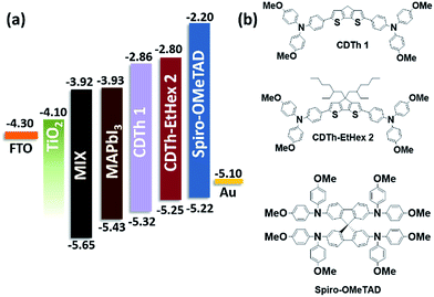
The two proposed HTMs (CDTh 1 and CDTh-EtHex 2) based on a 4H-cyclopenta[1,2-b:5,4-b′]dithiophene core were synthesized by a facile Pd-mediated Suzuki coupling reaction for PSC application. The chemical structures are depicted in Fig. 1 along with their energy level diagram, while the synthetic route is illustrated in Scheme 2.
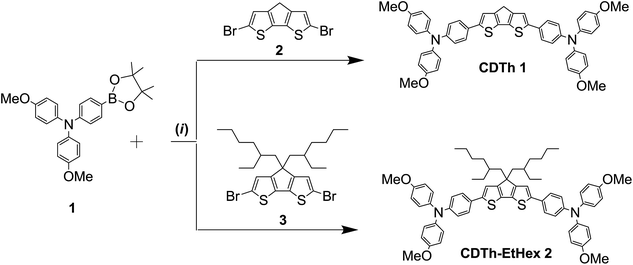 | ||
| Scheme 2 Synthetic route of CDTh 1 and CDTh-EtHex 2. (i) Suzuki coupling: Pd(PPh3)4, K2CO3, reflux in THF. | ||
4-Methoxy-N-(4-methoxyphenyl)-N-(4-(4,4,5,5-tetramethyl-1,3,2-dioxaborolan-2-yl)phenyl)aniline (compound 1 in Scheme 1) was synthesized as reported elsewhere,36,37 while the final compounds were synthesized through Suzuki–Miyaura cross coupling reactions, as illustrated below. The detailed synthesis of the intermediates 4-Methoxy-N-(4-methoxyphenyl)-N-(4-(4,4,5,5-tetramethyl-1,3,2-dioxaborolan-2-yl)phenyl)aniline (1), 4H-cyclopenta[1,2-b:5,4-b′]dithiophene (2) and 4,4-bis(2-ethylhexyl)-4H-cyclopenta[1,2-b:5,4-b′]dithiophene (3) of the final compound is reported in the ESI,† along with an estimation of the chemical cost of each intermediate and the final products.
The presence of alkyl substituents (2-ethylhexyl) on the cyclopentadithiophene core in CDTh-EtHex 2 enhances the solubility in organic solvents such as dichloromethane, chlorobenzene and toluene, and their influence on the optoelectronic and photovoltaic properties was studied. It is important to note that the cost estimation for the laboratory scale of these new HTMs, CDTh 1 (167.26 € g−1) and CDTh-EtHex 2 (179.05 € g−1), was found to be more than three times lower than that of Spiro-OMeTAD (∼600 € g−1).38Table 1 shows the summary of the optical, electrochemical and thermal properties of these synthesized molecules.
| HTM | λ max (nm) | ε (104 M−1 cm−1) | λ onset (nm) | E g (eV) | HOMO (eV) | LUMO (eV) | T d (°C) | T g (°C) |
|---|---|---|---|---|---|---|---|---|
| CDTh 1 | 442 | 6.08 | 502 | 2.47 | −5.32 | −2.86 | 325 | 200 |
| CDTh-EtHex 2 | 446 | 7.42 | 507 | 2.45 | −5.25 | −2.81 | 305 | 200 |
HTM property evaluation
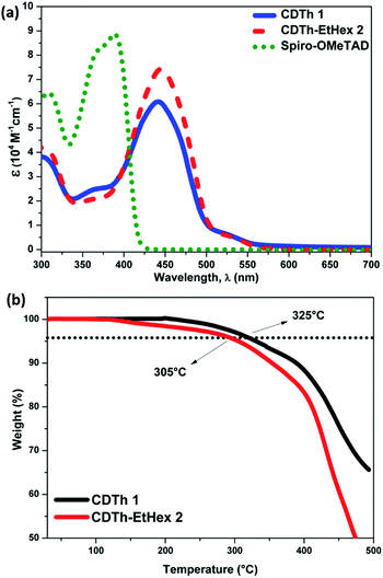
Fig. 2a shows the UV-visible absorption spectra of CDTh 1 and CDTh-EtHex 2 dissolved in dichloromethane and their optical parameters are listed in Table 1. CDTh 1 and CDTh-EtHex 2 exhibit main absorption peaks in the visible region at 442 and 446 nm respectively, which is due to the π–π* transition of the conjugated system, along with a hyperchromic shift for CDTh-EtHex 2. A side shoulder peak appears at 370 nm for both HTMs showing a little absorption in the UV-region. It can be deduced from the absorption spectra that the synthesized molecules show minimal absorption in the visible spectrum, which is an advantage to avoid reabsorption of the transmitted light and suggests their suitability also for an inverted configuration, as they will not compete with perovskite absorption for light harvesting. CDTh-EtHex 2 shows a higher extinction coefficient than CDTh 1. The λmax of both CDTh 1 and CDTh-EtHex 2 is slightly red shifted compared to the absorption peak of Spiro-OMeTAD (Fig. 2a), due to the cyclopentadithiophene core. Furthermore, CDTh-EtHex 2 shows an additional red shift with respect of CDTh 1, due to the presence of alkyl substituents on the thiophene-based core. The optical band gap (Eg) of the HTMs estimated from the λonset of the absorption is 2.47 eV and 2.45 eV, respectively. The electrochemical properties of CDTh 1 and CDTh-EtHex 2 were investigated using cyclic voltammetry experiments conducted (Fig. S3a†) in dichloromethane at room temperature [c ∼ 1 × 10⁻³ M] with TBAPF [0.1 M] as the supporting electrolyte.The HOMO energy level of CDTh 1 and CDTh-EtHex 2 was estimated from the first oxidation potential using the equation EHOMO = −4.4 − (Eox − E1/2(Fc/Fc+)), where Eox is the onset oxidation potential (vs. Fc/Fc+).39 Thus, the HOMO levels of CDTh 1 and CDTh-EtHex 2 were estimated to be −5.32 and −5.25 eV, respectively, which are little deeper than the HOMO level of Spiro-OMeTAD (−5.22 eV), leading to a better match with the valence band of both (FAPbI3)0.85(MAPbBr3)0.15 and MAPbI3 perovskites, and a relatively higher Voc (open circuit voltage) in PSCs than Spiro-OMeTAD. The lowest unoccupied molecular orbital (LUMO) level calculated using the expression ELUMO = EHOMO + Eg is −2.86 and −2.81 eV (Table 1) for CDTh 1 and CDTh-EtHex 2, respectively, which are slightly lower than the LUMO of Spiro-OMeTAD (−2.20 eV); however, they can still effectively block electron transfer from the perovskite to the Au electrode.
The CDTh-EtHex 2 shows the lowest oxidation potential, due to the presence of electron donating ethyl–hexyl substituents on the cyclopentadithiophene core, which might results in a faster hole extraction from the perovskite to the CDTh-EtHex 2. While the relatively higher oxidation potential for CDTh 1 will be advantageous for obtaining a high Voc.40
The thermal properties of the compounds, to study the stability of HTMs, were investigated by thermogravimetric analysis (TGA) and differential scanning calorimetry (DSC), (Fig. 2b and S3b†). The thermal decomposition temperatures (Td) were calculated from >5% mass loss in the second cycle of heating. A pre-heat cycle was also performed with the aim to eliminate possible humidity or impurities trapped in the material. The major thermal decomposition loss of CDTh 1 and CDTh-EtHex 2 were found to start around 325 °C and 305 °C respectively (Fig. 2b), which shows its excellent thermal stability. Fig. S2b,† illustrates the glass transition temperature (Tg) of CDTh 1 and CDTh-EtHex 2 and was found to be around 200 °C, which is higher than Spiro-OMeTAD (Tg = 120 °C)39 and indicates its higher stability in the amorphous state with respect to Spiro-OMeTAD, making them particularly suitable for PSCs commercial applications which demands tough thermal testing. The conductivity of these two HTMs was measured on substrates having interdigitating gold electrodes with a channel length of 2.5 μm. The HTMs were spin-coated onto the substrates from their corresponding solutions in chlorobenzene as described in the device fabrication section. The cobalt complex FK209 was added (6 mol%) to the HTM solution to chemically oxidize the HTM molecules. The corresponding current voltage (I–V) curves are shown in Fig. 3. The conductivity was calculated using Ohm's law. The calculated conductivity of undoped CDTh 1 and CDTh-EtHex 2 was 1.2 × 10⁻⁶ S cm−1 and 5.5 × 10⁻⁸ S cm−1 respectively. After doping with the cobalt complex FK209, the conductivity increased to 4.2 × 10⁻⁴ S cm−1 and 1 × 10⁻⁵ S cm−1 for CDTh 1 and CDTh-EtHex 2 respectively, which are 2–3 orders of magnitude higher than those of the undoped HTMs. In fact, the conductivity value of CDTh 1 was very close to the ones observed with doped Spiro-OMeTAD (σ = 4.06 × 10⁻⁴ S cm−1).
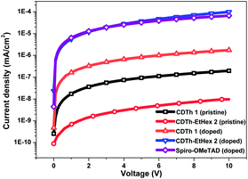 | ||
| Fig. 3 Semi-logarithmic current–voltage plot of CDTh 1, CDTh-EtHex 2 and Spiro-OMeTAD spin coated onto interdigitating gold electrodes. | ||
It is important to note that the cobalt complex (FK209) was not added as a dopant for HTM in the PSC fabrication; however it was added to the HTL for conductivity measurements, to oxidize the molecules. Since Spiro-OMeTAD performed better with the addition of the cobalt complex, the same amount was also added to CDTh 1 and CDTh-EtHex 2 in order to allow a more accurate comparison of conductivity.
The conductivity of CDTh 1 was one order of magnitude higher than that of CDTh-EtHex 2 (σ = 1.06 × 10⁻⁵ S cm−1). The higher conductivity of CDTh 1 might be explained by a better packing of the molecules in the film as the presence of bulky alkyl chains in CDTh-EtHex 2 may have an isolating effect and hinder intermolecular interactions.
Steady state PL measurement at the perovskite–HTM interface
In order to investigate the charge extraction in these HTMs at the perovskite/HTM interface, steady-state photoluminescence (PL) was measured (Fig. 4). Theoretically, the quenching of steady-state PL indicates efficient charge extraction. It was found that both HTMs, CDTh 1 and CDTh-EtHex 2, when deposited on perovskite layer, showed a higher PL quenching than the perovskite/Spiro-OMeTAD film. This suggests that these molecules can effectively extract holes from the perovskite at the perovskite/HTM interface.41 Moreover, CDTh-EtHex 2 showed relatively higher quenching efficiency than CDTh 1, which is in agreement with its lower oxidation potential due to its electron donating alkyl side group and thus allows a faster hole transfer from the perovskite to the HTM.39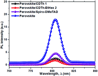 | ||
| Fig. 4 Photoluminescence (PL) emission spectra recorded for a bilayer of mixed perovskite (FAPbI3)0.85(MAPbBr3)0.15/HTMs upon excitation at 532 nm. | ||
Fabrication and characterization of perovskite solar cells
To exploit the practical utility of these newly developed CDTh 1 and CDTh-EtHex 2, they were integrated as HTMs for PSC fabrication using two different types of perovskites {MAPbI3 and (FAPbI3)0.85(MAPbBr3)0.15}. CDTh 1 and CDTh-EtHex 2 showed energetic level alignment with both the perovskites. The devices were fabricated in a mesoscopic configuration (Fig. 5) using the mixed cation–anion (FAPbI3)0.85(MAPbBr3)0.15 or pure MAPbI3 perovskite, with the structure of FTO/compact-TiO2 (30 nm)/mesoporous-TiO2 (80 nm)/(FAPbI3)0.85(MAPbBr3)0.15 (750 nm)/HTM (65 nm)/Au (80 nm) and FTO/compact-TiO2 (30 nm)/mesoporous-TiO2 (80 nm)/MAPbI3 (300 nm)/HTM (75 nm)/Au (80 nm) respectively. A well defined and sharp interface was observed for all the devices (Fig. 5) and this was in the accordance with the architecture adopted (Fig. 1a). Both types of perovskites were deposited using a one step method followed by a solvent engineering approach. The synthesis details and device fabrication steps are summarized in the ESI.† The noticeable difference between the perovskites is the thickness of the capping layer, which was found to be 750 nm and 300 nm respectively for (FAPbI3)0.85(MAPbBr3)0.15 and MAPbI3 (Fig. 5). Furthermore, the HTL thickness was estimated to be 65–70 nm in (FAPbI3)0.85(MAPbBr3)0.15-based devices and 75–80 nm for MAPbI3-based devices, while for both the perovskites, the HTM's concentration and spin-coating conditions were kept similar. Moreover, these two HTMs show similar viscosity, which allows having a comparable thickness of the deposited layers. The plausible reason for the difference in the thickness of HTMs for both the perovskites is due to the difference in the perovskite composition which may have dissimilar affinity towards the HTM structure.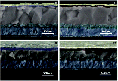 | ||
| Fig. 5 Cross-sectional SEM images of (a) mixed perovskite/CDTh 1, (b) mixed perovskite/CDTh-EtHex 2, (c) MAPbI3/CDTh 1, and (d) MAPbI3/CDTh-EtHex 2. | ||
For the hole transporting layer deposition, the synthesized HTMs were dissolved in chlorobenzene and only lithium bis(trifluoromethanesulfonyl)imide (LiTFSI) and 4-tert-butylpiridine (t-BP) additives were used without any cobalt complex dopant. However, it should be noted that Spiro-OMeTAD was used under the standard conditions, i.e., cobalt complex (FK209) dopant with LiTFSI and t-BP additives. Fig. S5† shows the cross-sectional SEM images of the mixed perovskite and MAPbI3 based devices using Spiro-OMeTAD as the HTM for comparison. The use of the cobalt dopant induces instability in PSCs and CDTh 1 and CDTh-EtHex 2 work efficiently without the use of FK209 as a dopant and yielded comparable performance to Spiro-OMeTAD. Moreover, the use of methoxy as an anchoring group and the sulphur from the thiophene moiety will interact strongly with perovskite iodine atoms and additionally the absence of UV absorbance will provide stability to the newly synthesized HTMs. More importantly, comparable PV performance can be reached for these HTMs just by using column-chromatography for purification, while in the case of Spiro-OMeTAD sublimation grade purification is required.
Fig. 6a shows the current density–voltage (J–V) curves of the fabricated devices using CDTh 1 and CDTh-EtHex 2 as HTMs and for comparison, Spiro-OMeTAD was also used in a reference device. The PV parameters for each configuration are summarized in Table 2, while the statistical data are listed in Table S3 (ESI).†
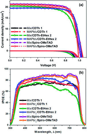 | ||
| Fig. 6 (a) Current density–voltage curves for devices based on CDTh 1, CDTh-EtHex 2 and Spiro-OMeTAD. (b) Incident photon-to-current conversion efficiency (IPCE) spectra of the devices. | ||
| Perovskite | HTM | R s (Ω cm2) | R sh (Ω cm2) | V oc (mV) | J sc (mA cm−2) | FF (%) | PCE (%) |
|---|---|---|---|---|---|---|---|
| a The additives used for the deposition of the hole transporting layer are as follows: for CDTh 1 and CDTh-EtHex 2, only LiTFSI and t-BP were used, while for Spiro-OMeTAD, LiTFSI, t-BP and FK209 dopants were used. | |||||||
| (FAPbI3)0.85(MAPbBr3)0.15 | CDTh 1 | 5.87 | 4004.16 | 980 | 20.81 | 70.63 | 14.35 |
| MAPbI3 | 6.08 | 2788.95 | 1030 | 20.53 | 70.84 | 15.01 | |
| (FAPbI3)0.85(MAPbBr3)0.15 | CDTh-EtHex 2 | 6.84 | 1486.07 | 1000 | 20.51 | 66.86 | 13.77 |
| MAPbI3 | 4.19 | 5228.89 | 1020 | 19.55 | 77.69 | 15.51 | |
| (FAPbI3)0.85(MAPbBr3)0.15 | Spiro-OMeTAD | 5.18 | 10![[thin space (1/6-em)]](https://www.rsc.org/images/entities/char_2009.gif) 256.24 256.24 |
1000 | 21.41 | 75.54 | 16.30 |
| MAPbI3 | 2.90 | 6074.17 | 980 | 21.16 | 78.08 | 16.19 | |
The devices based on MAPbI3 perovskite and CDTh 1 as HTMs with the configuration of FTO/compact-TiO2/mesoporous-TiO2/perovskite/HTM/Au showed a Jsc of 20.5 mA cm−2, a Voc of 1030 mV, a FF of 70.8%, a series resistance (Rs) of 6.08 Ω cm2 and a shunt resistance (Rsh) of 2788.95 Ω cm2, yielding a PCE of 15%, while the devices with the CDTh-EtHex 2 HTM showed improved photovoltaic behaviour, with a Jsc of 19.55 mA cm−2, a Voc of 1020 mV, a FF of 77.7%, a Rs of 4.1 Ω cm2 and a Rsh of 5228.89 Ω cm2 leading to an overall PCE of 15.5%. A slight decrease in Jsc and Voc was found while FF significantly enhanced to 77.7% compared to that of CDTh 1 and it can be attributed to the higher efficiency of CDTh-EtHex 2. The high FF is a result of low series resistance and high shunt resistance,42 which is consistent with our results. The value of series resistance and shunt resistance for all types of devices is reported in Table 2. For CDTh-EtHex 2, the Rs is very low and Rsh is very high as compared to those of CDTh 1 for the same thickness and doping level. Therefore, the improved performance of CDTh-EtHex 2 in MAPbI3 based PSCs can be ascribed to the low series and high shunt resistance. As the Rsh strongly relates to the leakage current due to the presence of pin holes or charge recombination,43,44 a high value of the Rsh in the case of CDTh-EtHex 2 in MAPbI3 based PSCs indicates lower leakage current than CDTh 1. The enhanced FF was also assumed to originate from the reduced interfacial charge recombination. The reference cell with Spiro-OMeTAD as the HTM exhibited 16.2% PCE.
The devices based on the mixed perovskite and CDTh 1 as HTMs showed improved performance compared to CDTh-EtHex 2 with a Jsc of 20.81 mA cm−2, a Voc of 980 mV, a FF of 70.63%, a series resistance (Rs) of 5.87 Ω cm2 and a shunt resistance (Rsh) of 4004.16 Ω cm2, yielding an overall PCE of 14.35%, while the devices with CDTh-EtHex 2 as the HTM showed a slightly lower performance and a PCE of 13.77% was achieved. The higher efficiency of CDTh 1 can be ascribed to the high value of FF.
One of the plausible reasons for this decrease in efficiency might be due to the high energy barrier (Eb) of 0.3–0.4 eV between the valence band of (FAPbI3)0.85(MAPbBr3)0.15 and the HOMO of CDTh 1 and CDTh-EtHex 2, while in the case of MAPbI3, the energy difference is 0.11–0.18 eV, and for favourable energy level matching, the energy difference (eV) should be in between 0.4 ≥ ΔE ≥ 0.10. The other possible reason might be due to the morphological difference between the perovskites with these new HTMs. A thin layer of the HTM (65–70 nm) was deposited atop of large grains of the mixed perovskite, as can be observed from cross sectional SEM images (Fig. 5a and b). This thin layer might not be sufficiently thick to cover uniformly the rough surface of the perovskite and leads to pinhole defects. Due to the presence of pinhole defects in the HTM layer, the perovskite can come in direct contact with the Au cathode, and will allow faster charge recombination, which degrades the perovskite as well as the cathode layer due to the chemical reaction between the iodide ions in the perovskite and metal cathode. Another possibility is the diffusion of the metal cathode into the perovskite resulting in a short-circuit of the device, which is further supported by a low value of Rsh with the mixed perovskite using the CDTh-EtHex 2 HTM, indicating increased interfacial charge recombination and therefore it showed low FF. Further optimization of perovskite and HTM layer thickness and dopant concentration is required to achieve improved efficiency in the case of mixed perovskite based PSCs.
The PV parameters extracted from the J–V curves recorded in the backward and forward scans are summarized in Table S3,† while the J–V curves along with the hysteresis index (HI) values are depicted in Fig. S3.† In the case of the MAPbI3, the least hysteresis can be seen with CDTh-EtHex 2 HTM based devices, while in the (FAPbI3)0.85(MAPbBr3)0.15 mixed perovskite, the lowest hysteresis was calculated for CDTh 1 based devices. Fig. 6b illustrates the incident photon-to-electron conversion efficiency (IPCE) spectra of the fabricated devices for each configuration. The IPCE spectra represent the percentage of extracted electrons per incident photon for each wavelength, and the integrated current for the devices is in close vicinity to the short circuit current density measured under 1 sun (Fig. S4, ESI†). The integrated current value is in good agreement with that of Spiro-OMeTAD-based devices, for both types of perovskites. This was also the case with CDTh-EtHex 2 based devices when fabricated using MAPbI3 as the perovskite layer. Although minute discrepancy in integrated Jsc was observed for CDTh 1 based devices in both the perovskites, it was in the acceptable range (Fig S4†) and can be further optimized by the measurement conditions.
In fact, the devices with mixed perovskite-based configurations showed a lower IPCE response in the range from 550 to 800 nm, compared to Spiro-OMeTAD based devices. This lower response could be due to the presence of traps and recombination sites at the perovskite/HTM interface,45 which is further supported by the thin layer of the HTM covered over the mixed perovskite causing pin hole defects and creating sites for recombination and further proved by the lower value of shunt resistance (Table 2). The presence of recombination sites and non-ideal interface could also influence the stability of the mixed/CDTh 1 and CDTh-EtHex 2 devices.
Additionally, a further possible reason for low IPCE at longer wavelengths could be due to the self-absorption of reflected light from gold.
Experimental
Device fabrication
All chemicals and reagent were purchased from Sigma-Aldrich and TCI and used without further purification. 2,2′,7,7′-Tetrakis(N,N-di-p-methoxy phenyamine)-9,9′-spirobifluorene (Spiro-OMeTAD) was purchased from Merck KGaA. Perovskite solar cell (PSC) devices were fabricated on laser etched FTO-coated glass (TEC, Pilkington). The substrates were cleaned by using an ultrasonication bath with Hellmanex, rinsed with deionized water, and then ultrasonicated in acetone and in 2-propanol and finally dried with compressed air. A TiO2 compact layer was deposited by spray pyrolysis at 450 °C using 1 mL of titanium diisopropoxide bis(acetyl acetonate) precursor solution (75% in 2-propanol, Sigma Aldrich) in 19 mL of pure ethanol using air as the carrier gas. After the blocking layer deposition, a TiO2 mesoporous layer (Dyesol paste, 30NRD) was deposited by spin coating (4000 rpm for 20 s) and then annealed at 500 °C for 30 min. Atop of this, methyl ammonium lead triiodide perovskite (MAPbI3) or a mixed cation halide perovskite ((FAPbI3)0.85(MAPbBr3)0.15) was deposited by a one step method followed by a solvent engineering approach. For the mixed cation halide perovskite, a 1.4 M mixture of lead iodide (PbI2) and lead bromide (PbBr2) and a mixture of formamidinium iodide (FAI) and methyl ammonium bromide (MABr) were dissolved in 4![[thin space (1/6-em)]](https://www.rsc.org/images/entities/char_2009.gif) :
:![[thin space (1/6-em)]](https://www.rsc.org/images/entities/char_2009.gif) 1 N,N-dimethylformamide (DMF)
1 N,N-dimethylformamide (DMF)![[thin space (1/6-em)]](https://www.rsc.org/images/entities/char_2009.gif) :
:![[thin space (1/6-em)]](https://www.rsc.org/images/entities/char_2009.gif) dimethyl sulfoxide (DMSO) solution, while for the pure methyl ammonium perovskite, a 1.2 M solution of PbI2 in DMSO was left under stirring overnight at 80 °C to promote the proper dissolution of lead iodide; then, a stoichiometric amount of methyl ammonium iodide was added and properly mixed by stirring for 10 minutes. The perovskite precursor solution was spin-coated on top of the mesoporous layer at 1000 rpm for 10 seconds and then at 6000 rpm for 30 seconds. During the second step, chlorobenzene was dripped in the centre of the substrate during the last 10 seconds. After solvent treatment, the films were transferred onto a hotplate and annealed at 100 °C for 1 hour. A 60 mM solution of CDTh 1, CDTh-EtHex 2 and Spiro-OMeTAD was prepared by dissolving an appropriate amount of the HTMs in 1 mL of chlorobenzene, and standard additives of 17.5 μL of a lithium bis(trifluoromethylsulphonyl)imide (LiTFSI) solution prepared from a stock solution (520 mg of LiTFSI in 1 mL of acetonitrile) and 28.8 μL of 4-tert-butylpyridine (t-BP) were added. 21.9 μL of a FK209 (tris(2-(1H-pyrazol-1-yl)-4-tert-butylpyridine)-cobalt(III)tris(bis(trifluoro-methylsulfonyl)imide)) solution prepared from a stock solution (400 mg in 1 mL of acetonitrile) was added only to the Spiro-OMeTAD solution. Then 35 μL of each HTM solution were dropped on the perovskite substrates of the solar cell samples described above and the samples were spin coated at 4000 rpm for 20 seconds. After that, 80 nm of gold was thermally evaporated on top of HTMs under a vacuum level between 10−6 and 10−5 torr and used as the cathode. All the solutions were prepared inside an argon filled glove box under controlled moisture and oxygen conditions (H2O level: <1 ppm and O2 level: <5 ppm).
dimethyl sulfoxide (DMSO) solution, while for the pure methyl ammonium perovskite, a 1.2 M solution of PbI2 in DMSO was left under stirring overnight at 80 °C to promote the proper dissolution of lead iodide; then, a stoichiometric amount of methyl ammonium iodide was added and properly mixed by stirring for 10 minutes. The perovskite precursor solution was spin-coated on top of the mesoporous layer at 1000 rpm for 10 seconds and then at 6000 rpm for 30 seconds. During the second step, chlorobenzene was dripped in the centre of the substrate during the last 10 seconds. After solvent treatment, the films were transferred onto a hotplate and annealed at 100 °C for 1 hour. A 60 mM solution of CDTh 1, CDTh-EtHex 2 and Spiro-OMeTAD was prepared by dissolving an appropriate amount of the HTMs in 1 mL of chlorobenzene, and standard additives of 17.5 μL of a lithium bis(trifluoromethylsulphonyl)imide (LiTFSI) solution prepared from a stock solution (520 mg of LiTFSI in 1 mL of acetonitrile) and 28.8 μL of 4-tert-butylpyridine (t-BP) were added. 21.9 μL of a FK209 (tris(2-(1H-pyrazol-1-yl)-4-tert-butylpyridine)-cobalt(III)tris(bis(trifluoro-methylsulfonyl)imide)) solution prepared from a stock solution (400 mg in 1 mL of acetonitrile) was added only to the Spiro-OMeTAD solution. Then 35 μL of each HTM solution were dropped on the perovskite substrates of the solar cell samples described above and the samples were spin coated at 4000 rpm for 20 seconds. After that, 80 nm of gold was thermally evaporated on top of HTMs under a vacuum level between 10−6 and 10−5 torr and used as the cathode. All the solutions were prepared inside an argon filled glove box under controlled moisture and oxygen conditions (H2O level: <1 ppm and O2 level: <5 ppm).
Conclusions
In summary, by molecular engineering, we have designed and synthesized simple yet effective small-molecule based p-type organic semiconductors. We have revealed that a minute alteration in the chemical structure affected the optoelectronic properties of HTMs and influenced the PV properties significantly. The high thermal stability of these novel HTMs was due to the insertion of a functionalized cyclopentadithiophene core. CDTh 1 and CDTh-EtHex 2 were synthesized using a simple Pd-catalyzed Suzuki coupling and purified by a simple route with a high yield. In these molecules, column-chromatography grade purification is sufficient to reach comparable photovoltaic behaviour to Spiro-OMeTAD, which requires a sublimation grade purification. The facile synthesis and simple purification process of the presented HTMs will also allow reaching low synthetic costs and a wide market penetration. Photoluminescence quenching indicates that both HTMs, CDTh 1 and CDTh-EtHex 2, can efficiently extract holes from perovskites. The photovoltaic characteristics obtained with the newly designed HTMs, CDTh 1 and CDTh-EtHex 2, were tested in two different types of perovskites and they were found to be on a par with Spiro-OMeTAD, even without additional additives such as cobalt-complex dopants. Additives help to achieve higher open circuit voltage, but at the cost of device stability. Due to their facile synthesis, purification process and performance in devices, CDTh 1 and CDTh-EtHex 2 are potentially attractive candidates to replace the cost ineffective Spiro-OMeTAD.Author contributions
LC carried out all the experiments and compiled the graphs and SK performed the opto-electrical characterization and analysis of data and provided guidance to LC. IZ performed conductivity measurements and MKN supervised them and analysed the data. MS provided support for device fabrication and chemical structure experiments. S. A. directed and coordinated the research. All authors contributed to the completion of the final document.Conflicts of interest
There are no conflicts to declare.Acknowledgements
This project has received funding from the European Union Seventh Framework Programme under grant agreement no. [Thinface, 607232] and was also supported by a European Research council grant [MOLEMAT, 72630].Notes and references
- A. Kojima, K. Teshima, Y. Shirai and T. Miyasaka, J. Am. Chem. Soc., 2009, 131, 6050–6051 CrossRef PubMed.
- S. Kazim, M. K. Nazeeruddin, M. Graetzel and S. Ahmad, Angew. Chem. Int. Ed., 2014, 53, 2812–2824 ( Angew. Chem. , 2014 , 126 , 2854–2867 ) CrossRef PubMed.
- X. Li, D. Bi, C. Yi, J.-D. Decoppet, J. Luo, S. M. Zakeeruddin, A. Hagfeldt and M. Graetzel, Science, 2016, 353, 58–62 CrossRef PubMed.
- M. Salado, L. Calio, R. Berger, S. Kazim and S. Ahmad, Phys. Chem. Chem. Phys., 2016, 18, 27148–27157 RSC.
- C. Quarti, E. Mosconi, P. Umari and F. De Angelis, Inorg. Chem., 2017, 56, 74–83 CrossRef PubMed.
- A. Todinova, J. Idígoras, M. Salado, S. Kazim and J. A. Anta, J. Phys. Chem. Lett., 2015, 6, 3923–3930 CrossRef PubMed.
- S. Yang, W. Fu, Z. Zhang, H. Chen and C.-Z. Li, J. Mater. Chem. A, 2017, 5, 11462–11482 Search PubMed.
- F. De Angelis and P. V. Kamat, ACS Energy Lett., 2017, 2, 922–923 CrossRef.
- N.-G. Park, Mater. Today, 2015, 18, 65–72 CrossRef.
- W. S. Yang, B.-W. Park, E. H. Jung, N. J. Jeon, Y. C. Kim, D. U. Lee, S. S. Shin, J. Seo, E. K. Kim, J. H. Noh and S. Il Seok, Science, 2017, 356, 1376–1379 CrossRef PubMed.
- A. Binek, M. L. Petrus, N. Huber, H. Bristow, Y. Hu, T. Bein and P. Docampo, ACS Appl. Mater. Interfaces, 2016, 8, 12881–12886 Search PubMed.
- N. J. Jeon, J. H. Noh, W. S. Yang, Y. C. Kim, S. Ryu, J. Seo and S. Il Seok, Nature, 2015, 517, 476–480 CrossRef PubMed.
- F. Javier Ramos, M. Ince, M. Urbani, A. Abate, M. Graetzel, S. Ahmad, T. Torres and M. K. Nazeeruddin, Dalton Trans., 2015, 44, 10847–10851 RSC.
- L. Caliò, J. F. Berna, S. Kazim, M. Madsen, H.-G. Rubahn, A. Sastre-Santos and S. Ahmad, Sustainable Energy Fuels, 2017, 1, 2071–2077 Search PubMed.
- G. Yang, Y. Wang, J. Xu, H. Lei, C. Chen and H. Shan, Nano Energy, 2017, 31, 322–330 CrossRef.
- L. Calió, S. Kazim, M. Graetzel and S. Ahmad, Angew. Chem. Int. Ed., 2016, 55, 14522–14545 ( Angew. Chem. , 2016 , 128 , 14740–14764 ) CrossRef PubMed.
- T. Matsui, I. Petrikyte, T. Malinauskas, K. Domanski, M. Daskeviciene, M. Steponaitis, P. Gratia, W. Tress, J. P. Correa-Baena, A. Abate, A. Hagfeldt, M. Grätzel, M. K. Nazeeruddin, V. Getautis and M. Saliba, ChemSusChem, 2016, 9, 2567–2571 CrossRef PubMed.
- I. Lim, E.-K. Kim, S. A. Patil, D. Y. Ahn, W. Lee, N. K. Shrestha, J. K. Lee, W. K. Seok, C.-G. Cho and S.-H. Han, RSC Adv., 2015, 5, 55321–55327 RSC.
- K. T. Cho, O. Trukhina, C. Roldán-Carmona, M. Ince, P. Gratia, G. Grancini, P. Gao, T. Marszalek, W. Pisula, P. Y. Reddy, T. Torres and M. K. Nazeeruddin, Adv. Energy Mater., 2017, 7, 1601733 CrossRef.
- X. Yin, L. Guan, J. Yu, D. Zhao, C. Wang, N. Shrestha, Y. Han, Q. An, J. Zhou, B. Zhou, Y. Yu, C. R. Grice, R. A. Awni, F. Zhang, J. Wang, R. J. Ellingson, Y. Yan and W. Tang, Nano Energy, 2017, 40, 163–169 CrossRef.
- I. Petrikyte, I. Zimmermann, K. Rakstys, M. Daskeviciene, T. Malinauskas, V. Jankauskas, V. Getautis and M. K. Nazeeruddin, Nanoscale, 2016, 8, 8530–8535 RSC.
- F. J. Ramos, K. Rakstys, S. Kazim, M. Grätzel, M. K. Nazeeruddin and S. Ahmad, RSC Adv., 2015, 5, 53426–53432 RSC.
- L. Calió, C. Momblona, L. Gil-Escrig, S. Kazim, M. Sessolo, Á. Sastre-Santos, H. J. Bolink and S. Ahmad, Sol. Energy Mater. Sol. Cells, 2017, 163, 237–241 CrossRef.
- R. Grisorio, R. Iacobellis, A. Listorti, L. De Marco, M. P. Cipolla, M. Manca, A. Rizzo, A. Abate, G. Gigli and G. P. Suranna, ACS Appl. Mater. Interfaces, 2017, 9, 24778–24787 Search PubMed.
- A. Abate, S. Paek, F. Giordano, J. P. Correa-Baena, M. Saliba, P. Gao, T. Matsui, J. Ko, S. M. Zakeeruddin, K. H. Dahmen, A. Hagfeldt, M. Grätzel and M. K. Nazeeruddin, Energy Environ. Sci., 2016, 8, 2946–2953 Search PubMed.
- H. Li, K. Fu, P. P. Boix, L. H. Wong, A. Hagfeldt, M. Graetzel, S. G. Mhaisalkar and A. C. Grimsdale, ChemSusChem, 2014, 7, 3420–3425 CrossRef PubMed.
- P. Ganesan, K. Fu, P. Gao, I. Raabe, K. Schenk, R. Scopelliti, J. Luo, L. H. Wong, M. Grätzel and M. K. Nazeeruddin, Energy Environ. Sci., 2015, 8, 1986–1991 Search PubMed.
- Y. Ding, Y. Jiang, W. Zhang, L. Zhang, X. Lu, Q. Wang, G. Zhou, J. M. Liu, K. Kempa and J. Gao, J. Phys. Chem. C, 2017, 121, 16731–16738 Search PubMed.
- Q. Lin, W. Jiang, S. Zhang, R. C. R. Nagiri, H. Jin, P. L. Burn and P. Meredith, ACS Appl. Mater. Interfaces, 2017, 9, 9096–9101 Search PubMed.
- P. Y. Su, Y. F. Chen, J. M. Liu, L. M. Xiao, D. Bin Kuang, M. Mayor and C. Y. Su, Electrochim. Acta, 2016, 209, 529–540 CrossRef.
- T. Krishnamoorthy, F. Kunwu, P. P. Boix, H. Li, T. Ming Koh, A. Wei Lin Leong, S. Powar, A. Grimsdale, M. G. Atzel, N. Mathews and S. G. Mhaisalkar, J. Mater. Chem. A, 2014, 2, 6305–6309 Search PubMed.
- X. Liu, F. Kong, F. Guo, T. Cheng, W. Chen, T. Yu, J. Chen, Z. Tan and S. Dai, Dyes Pigm., 2017, 139, 129–135 CrossRef.
- S. Paek, I. Zimmermann, P. Gao, P. Gratia, K. Rakstys, G. Grancini, M. K. Nazeeruddin, M. A. Rub, S. A. Kosa, K. A. Alamry and A. M. Asiri, Chem. Sci., 2016, 7, 6068–6075 RSC.
- M. Saliba, S. Orlandi, T. Matsui, S. Aghazada, M. Cavazzini, J.-P. Correa-Baena, P. Gao, R. Scopelliti, E. Mosconi, K.-H. Dahmen, F. De Angelis, A. Abate, A. Hagfeldt, G. Pozzi, M. Graetzel and M. K. Nazeeruddin, Nat. Energy, 2016, 1, 15017 CrossRef.
- A. Torres and L. G. C. Rego, J. Phys. Chem. C, 2014, 118, 26947–26954 Search PubMed.
- X. Liu, F. Kong, Z. Tan, T. Cheng, W. Chen, T. Yu, F. Guo, J. Chen, J. Yao and S. Dai, RSC Adv., 2016, 6, 87454–87460 RSC.
- R. A. Belisle, P. Jain, R. Prasanna, T. Leijtens and M. D. McGehee, ACS Energy Lett., 2016, 1, 556–560 CrossRef.
- F. Zhang, X. Liu, C. Yi, D. Bi, J. Luo, S. Wang, X. Li, Y. Xiao, S. M. Zakeeruddin and M. Graetzel, ChemSusChem, 2016, 9, 2578–2585 CrossRef PubMed.
- N. G. Connelly and W. E. Geiger, Chem. Rev., 1996, 96, 877–910 CrossRef PubMed.
- Y. Yang, Y. Liu, Z. Hong, Q. Chen, H. Chen, W. H. Chang and T. Bin Song, Adv. Mater., 2016, 28, 440–446 CrossRef PubMed.
- G. Xing, N. Mathews, S. Sun, S. S. Lim, Y. M. Lam, M. Gratzel, S. Mhaisalkar and T. C. Sum, Science, 2013, 342, 344–347 CrossRef PubMed.
- K. Rajkanan and J. Shewchun, Solid-State Electron., 1979, 22, 193–197 CrossRef.
- W. J. Potscavage, A. Sharma and B. Kippelen, Acc. Chem. Res., 2009, 42, 1758–1767 CrossRef PubMed.
- S. Kazim, F. J. Ramos, P. Gao, M. K. Nazeeruddin, M. Grätzel and S. Ahmad, Energy Environ. Sci., 2015, 8, 1816–1823 Search PubMed.
- M. Salado, J. Idigoras, L. Calio, S. Kazim, M. K. Nazeeruddin, J. A. Anta and S. Ahmad, ACS Appl. Mater. Interfaces, 2016, 8, 34414–34421 Search PubMed.
Footnote |
| † Electronic supplementary information (ESI) available. See DOI: 10.1039/c8se00119g |
| This journal is © The Royal Society of Chemistry 2018 |


