Semiconductor self-assembled monolayers as selective contacts for efficient PiN perovskite solar cells†
E.
Yalcin
a,
M.
Can
b,
C.
Rodriguez-Seco
c,
E.
Aktas
 c,
R.
Pudi
c,
W.
Cambarau
c,
S.
Demic
*a and
E.
Palomares
c,
R.
Pudi
c,
W.
Cambarau
c,
S.
Demic
*a and
E.
Palomares
 *cd
*cd
aIzmir Katip Celebi University, Department of Material Science and Engineering, Izmir, Turkey
bIzmir Katip Celebi University, Department of Engineering Sciences, Izmir, Turkey
cInstitute of Chemical Research of Catalonia (ICIQ), Barcelona Institute of Science and Technology, Avda. Països Catalans, 16, E-43007, Tarragona, Spain. E-mail: epalomares@iciq.es
dICREA, Passeig Lluis Companys, 28, E-08018, Barcelona, Spain
First published on 3rd October 2018
Abstract
Herein, we studied the use of two different Self Assembled Monolayers (SAMs) made of semiconductor hole transport organic molecules to replace the most common p-type contact, PEDOT:PSS, in PiN methyl ammonium lead iodide perovskite solar cells (PSCs). The SAM molecule (MC-43) leads to a solar to energy conversion efficiency of 17.3, which is among the highest efficiencies reported to date for PiN perovskite solar cells. The present finding highlights the potential of semiconductor based SAMs to fabricate stable and high performing planar PSCs.
Broader contextHybrid semiconductor perovskite materials are often sandwiched between a selective material used as a contact for electrons (ETM: electron transport material) and a selective material used as a contact for holes (HTM: hole transport material) to fabricate an efficient solar cell. For instance, in so called “inverted” perovskite solar cells the ETM is a fullerene derivative and the HTM is a polymer, such as PEDOT:PSS. However, the instability of these solar cells – due frequently to the ionic nature of the PEDOT:PSS – presents the challenge to find a more suitable HTM. In this work, we show how organic molecules, with the property of forming self-assemble monolayers, became an efficient selective contact to transport holes and make it possible to obtain devices reaching efficiencies over 17% under standard measurement conditions. Moreover, the fine tuning of the molecule structure offers the possibility to study molecular structure vs. solar cell parameters in depth. |
Introduction
The research activity in hybrid lead based perovskite solar cells has increased enormously since the pioneering work of Miyasaka and co-workers.1 For instance, the record in power conversion efficiency (PCE) has grown exponentially up to the current 22.7%.2 Moreover, the fine-tuning of material composition had led to considerable improvements in device stability,3,4 encouraging its pre-industrialization. In this context, several research groups are committed to the development of new methods to grow and form homogeneous perovskite films5–11 with bigger grain size and limited defects in order to achieve highly reproducible devices with the maximum PCE. The use of different halides and organic–inorganic cations, mixed in such a way that it promotes the final perovskite structure, had led to a variety of materials with different valence band and conduction band energy levels, and improved ionic and electronic transport capabilities.12 Yet, the use of appropriate selective contacts,13 either organic molecules or metal oxides, also plays a crucial role in reducing charge recombination losses and maximizing the open-circuit voltage (VOC) and thus the PCE.The configurations of perovskite solar cells (PSCs) are frequently known as ‘regular’ (or NiP), where the perovskite absorber is deposited on top of the electron transport material (ETM), or ‘inverted’ (PiN) structures, where, on the contrary, the perovskite layer is on top of the hole transport material (HTM). The latter has been essentially developed to offer an alternative to the conventional structure14 which presents some drawbacks related to the charge transport materials, like the high processing temperature of TiO2 (the most employed ETM) or the complex doping system of the HTM (usually spiro-OMeTAD or PTAA) as much as its cost. Nonetheless, the regular structure remains the most employed architecture and still holds the record efficiency in PSCs.
The inverted structure offers the advantage of low-temperature processing that allows the fabrication of perovskite modules on flexible substrates compatible with the roll-to-roll technology.15 The typical inverted configuration, which has been already reported with efficiencies as high as 18%,6,16 consists of poly(3,4-ethylenedioxythiophene):poly(styrenesulfonate) (PEDOT:PSS) as the HTM and [6,6]-phenyl-C(61)-butyric acid methyl ester (PC60BM) or its corresponding C70 derivative, PC70BM, as the ETL. However, besides its excellent optoelectronic properties, PEDOT:PSS suffers from acidic and hygroscopic characteristics that can severely compromise the stability of the devices. Numerous inorganic alternatives to PEDOT:PSS, like nickel-based or copper-based semiconductors,17 have been considered and successfully employed as the HTM in PSCs.
In this framework, self-assembled monolayers (SAMs) of organic molecules on electrodes surfaces have been considered as a valid alternative to conventional single-carrier transport layers.4,18–22
SAMs are small molecules that can be chemically attached to a surface (typically a metal or a metal oxide) and form extremely thin and stable layers. Besides their facile synthesis and deposition, the main advantage of SAMs is the ability to tune the electrical properties of the surface on which they are attached. This ability allows modulating the work function (WF) of a metal oxide, working as an electrode in a solar cell, in order to align it with the energy level of the photo-excited quasi-Fermi levels of the active layer.
This fact is a key point to ensure an ohmic contact at the interface and to maximize the VOC. In the literature, the number of successful uses of SAMs in PSCs is scarce. Zuo et al.21 demonstrate that an extremely thin layer of propanoic acid-based SAMs attached on top of a ZnO ETM can significantly increase the device PCE due to a better energy alignment with the perovskite LUMO and improved film crystallinity. Yang and co-workers23 successfully employed (3-aminopropyl)triethoxysilane (APTES) as a SAM material to modify the SnO2 ETM, achieving 18% efficiency in a planar NiP PSC. Likewise, in our previous work we prove that the use of simple boronic acid-based SAMs, for coating the compact TiO2 surface, is able to improve the photovoltaic properties of a methyl ammonium lead iodide (MAPbI3 or MAPI) PSC.18 In this work, we move one step further and together with the property of being capable to form organized molecular layers we introduce the semiconductor feature for efficient transport of electronic holes. Our synthesised molecules, namely TPA and MC-43, are depicted in Fig. 1a and b, and are directly assembled at the indium doped tin oxide (ITO) electrode as surface modifiers to enhance hole extraction in inverted PSCs.
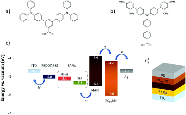 | ||
| Fig. 1 The molecular structure of (a) TPA and (b) MC-43. (c) Energy levels of the PSC materials employed in this study. (d) Layered structure of the SAM based device. | ||
We studied the influence of the SAMs on the surface wettability, the perovskite formation and the photovoltaic performance of the solar cells. Our results show that it is possible to obtain high efficiencies in PiN perovskite based solar cells without the need of any inorganic metal oxide or semiconductor polymer as the HTM.
Experimental section
General procedure for synthesis of TPA
The synthesis of the TPA molecule was first performed by the Can et al. group and its detailed synthetic procedure was reported previously.24 The general protocol is as follows: a Suzuki cross-coupling procedure was applied to a DME solution of methyl 3,5-dibromobenzoic acid (0.62 mmol), 4-(diphenyl amino)phenylboronic acid (1.35 mmol), Pd(PPh3)4 (0.04 mmol), and K2CO3 (5.00 mmol). After degassing, the mixture was refluxed for 16 h under argon and then cooled to RT. The crude product after evaporating the combined extractions (DCM) was purified by silica gel column chromatography (hexane![[thin space (1/6-em)]](https://www.rsc.org/images/entities/char_2009.gif) :
:![[thin space (1/6-em)]](https://www.rsc.org/images/entities/char_2009.gif) ethyl acetate, 1
ethyl acetate, 1![[thin space (1/6-em)]](https://www.rsc.org/images/entities/char_2009.gif) :
:![[thin space (1/6-em)]](https://www.rsc.org/images/entities/char_2009.gif) 2). The pure compound was then hydrolyzed by KOH (1 mL, 2 N) by refluxing in a THF/MeOH mixture. Then, the cooled mixture was acidified by HCl (1 mL, 2 N). The product was collected by filtration and used without further purification. 1H NMR (400 MHz, CDCl3, ppm) 8.23 (dd, H), 7.67–7.71 (dd, 2H), 7.56–7.59 (m, 8H), 7.41–7.43 (s, 8H), 7.10–7.12 (m, 12H).
2). The pure compound was then hydrolyzed by KOH (1 mL, 2 N) by refluxing in a THF/MeOH mixture. Then, the cooled mixture was acidified by HCl (1 mL, 2 N). The product was collected by filtration and used without further purification. 1H NMR (400 MHz, CDCl3, ppm) 8.23 (dd, H), 7.67–7.71 (dd, 2H), 7.56–7.59 (m, 8H), 7.41–7.43 (s, 8H), 7.10–7.12 (m, 12H).
General procedure for synthesis of MC-43
The schematic representation of the synthetic route for MC-43 is illustrated in Fig. S2 (ESI†).![[thin space (1/6-em)]](https://www.rsc.org/images/entities/char_2009.gif) :
:![[thin space (1/6-em)]](https://www.rsc.org/images/entities/char_2009.gif) 1) mixture was added to maintain complete dissolution at 80 °C. After stirring for 12 h at room temperature, the reaction mixture was subjected to vacuum and the residue was dissolved in water. After washing the aqueous phase containing the salt of the crude product with ethyl acetate several times, the aqueous phase was acidified with formic acid and subsequently extracted with ethyl acetate (3 × 25 mL). The combined organic layers were dried over sodium sulphate. Removal of the solvent provided the crude product of MC-43, which was then used without further purification. 1H NMR (300 MHz, DMSO) δH: 8,00 (d, 2H); 7.71 (dd, 4H); 7.45 (dd, 4H); 7.26 (d, 2H); 7.12 (dd, 6H); 6,66 (d, 2H); 6.62 (dd, 2H); 3.80 (s, 6H); 3.78 (s, 6H). 13C-NMR (125 MHz, DMSO); δC 160.37, 157.56, 147.69, 145.55, 133.58, 131.19, 130.70, 130.33, 128.32, 126.07, 124.35, 123.49, 122.23, 105.79, 99.40, 55.99, 55.72.
1) mixture was added to maintain complete dissolution at 80 °C. After stirring for 12 h at room temperature, the reaction mixture was subjected to vacuum and the residue was dissolved in water. After washing the aqueous phase containing the salt of the crude product with ethyl acetate several times, the aqueous phase was acidified with formic acid and subsequently extracted with ethyl acetate (3 × 25 mL). The combined organic layers were dried over sodium sulphate. Removal of the solvent provided the crude product of MC-43, which was then used without further purification. 1H NMR (300 MHz, DMSO) δH: 8,00 (d, 2H); 7.71 (dd, 4H); 7.45 (dd, 4H); 7.26 (d, 2H); 7.12 (dd, 6H); 6,66 (d, 2H); 6.62 (dd, 2H); 3.80 (s, 6H); 3.78 (s, 6H). 13C-NMR (125 MHz, DMSO); δC 160.37, 157.56, 147.69, 145.55, 133.58, 131.19, 130.70, 130.33, 128.32, 126.07, 124.35, 123.49, 122.23, 105.79, 99.40, 55.99, 55.72.
HRMS (ESI+) m/z calcd 636.2405 for C42H30N5O2, found 636.2394.
Device fabrication
All materials were purchased from Sigma-Aldrich and used as received unless differently specified. ITO coated glasses (Xinyan technology Ltd, 15 Ω per square) were properly cleaned by ultrasonication in water with Hellmanex™ detergent, then in acetone and finally in isopropanol. TPA and MC-43 were dissolved in toluene (4 × 10⁻⁴ M) and kept stirring at 60 °C for 2 h. ITO substrates were treated with UV/ozone for 30 min and subsequently immersed in SAM solutions for 4 h. After that, substrates were rinsed with toluene to remove residual SAM molecules which are not strongly bonded on the ITO surface. Alternatively, PEDOT:PSS (Clevios™ PV P AI4083, Heraeus) was deposited as the HTM at a 4500 rpm spin speed for 30 s, achieving a thickness of 25–30 nm. Finally, the substrates were transferred in a nitrogen-filled glovebox to complete the device fabrication.For the preparation of perovskite solution, 460 mg of lead(II) iodide (PbI2, 99.995%, Alfa Aesar) was dissolved in (920![[thin space (1/6-em)]](https://www.rsc.org/images/entities/char_2009.gif) :
:![[thin space (1/6-em)]](https://www.rsc.org/images/entities/char_2009.gif) 80) L of an anhydrous DMF
80) L of an anhydrous DMF![[thin space (1/6-em)]](https://www.rsc.org/images/entities/char_2009.gif) :
:![[thin space (1/6-em)]](https://www.rsc.org/images/entities/char_2009.gif) DMSO mixture while 50 mg of methylammonium iodide (MAI, Greatcell Solar Ltd) was dissolved in 1 mL of anhydrous isopropanol. The solutions were kept stirring for 2 h. The perovskite was obtained with a two-step deposition method. In the first step, after filtering the solution with a 0.22 μm PTFE filter, 70 μL of PbI2 was cast at 4000 rpm. After 60 s, 100 μL of MAI was dripped over the spinning substrate. The substrate was kept spinning for a further 30 s. Successively, substrates were moved directly onto a hotplate and annealed for 10 min at 100 °C. The thickness achieved is around 350 nm.
DMSO mixture while 50 mg of methylammonium iodide (MAI, Greatcell Solar Ltd) was dissolved in 1 mL of anhydrous isopropanol. The solutions were kept stirring for 2 h. The perovskite was obtained with a two-step deposition method. In the first step, after filtering the solution with a 0.22 μm PTFE filter, 70 μL of PbI2 was cast at 4000 rpm. After 60 s, 100 μL of MAI was dripped over the spinning substrate. The substrate was kept spinning for a further 30 s. Successively, substrates were moved directly onto a hotplate and annealed for 10 min at 100 °C. The thickness achieved is around 350 nm.
After perovskite film preparation, the devices were stored in the glovebox overnight in the dark. Afterwards, 20 mg of PC60BM (Nano-C Inc.) was dissolved in 1 mL of anhydrous chlorobenzene, stirred for 2 h and deposited via spin coating (static dispensing, 70 μL) at 2000 rpm for 30 s achieving a thickness of around 60 nm. Finally, 120 nm of Ag (Kurt J. Lesker) was deposited by thermal evaporation under high vacuum (around 1 × 10⁻⁶ mbar).
Device characterization
Contact angle measurements were carried out with a KSV Attension Theta Lite optical tensiometer, used in a sessile water drop experiment. It was performed by dispensing a water droplet with an average volume of 4 μL onto the sample surface and measuring in the static state.Atomic force microscopy measurement was employed to analyze the surface topography of modified and bare ITO. Measurements were performed using a Nanosurf Easyscan-2 controller AFM in non-contact mode.
Cyclic voltammetry was conducted by means of a CH Instrument CHI440b potentiostat to determine the electrochemical behavior of modified ITO surfaces.
The X-ray photoelectron spectroscopy (XPS) characterization was carried out with PHI 5000 VersaProbe equipment.
The J–V curves were measured using a solar simulator (ABET 11000) and a source meter (Keithley 2400). The curves were registered under 1 sun conditions (100 mW cm−2, AM 1.5G) calibrated with a silicon photodiode (NREL). The active area of the devices was 0.09 cm2.
The EQE spectrum was measured using a homemade set up consisting of a 150 W Oriel xenon lamp, a motorized monochromator and a Keithley 2400 digital source meter. The photocurrent and irradiated light intensity were measured simultaneously and processed with home-built Labview software.
Results and discussion
SAM modification of the ITO surface
Fig. 1d shows a schematic device structure of a PiN type planar MAPI perovskite solar cell composed of a transparent conductive ITO layer followed by a SAM modification layer, MAPbI3, PC60BM and finally a silver electrode. The SAM coating on ITO is obtained with a straightforward procedure, consisting of submerging the substrate into a solution containing the molecule for an appropriate time, enough for the monolayers to attach to the ITO surface and form a compact and ordered film. The drawing proposed in Fig. 2 illustrates how to obtain a SAM modified ITO surface on a conventional sodalime© glass substrate and the remaining steps to complete the device.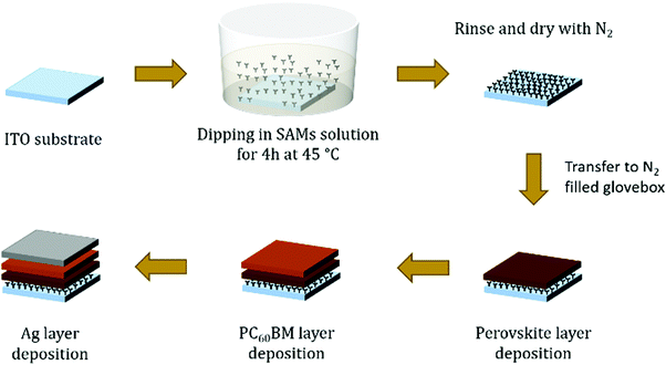 | ||
| Fig. 2 Illustration of the device preparation steps. The ITO substrates are treated with UV–ozone before SAM deposition. | ||
Cyclic voltammetry was used to determine the electrochemical behaviour of TPA and MC-43 coated ITO surfaces. The new energy level (HOMO) of TPA and MC-43 modified ITO was determined as 5.33 and 5.11 eV respectively from the inflection point of the cyclic voltammograms given in Fig. S1 (see ESI†).
It is worth noting that the presence of electron-donating groups coupled to the triphenylamine backbone reduces its oxidation potential. This is a possible explanation for the 0.2 eV difference in the HOMO level between ITO/MC-43 and ITO/TPA surfaces.
The surface wettability of the ITO coated substrate before and after modification with the SAMs was investigated by measuring the contact angle in a sessile water drop experiment. It is well known that the ITO surface has a hydrophilic character. The contact angle on a bare ITO surface (i.e. without SAM coating) was estimated as 53.6° as shown in Fig. 3a. The same picture shows, as a comparison, that TPA and MC-43 modified ITO surfaces became more hydrophobic (around 85° and 90°) with the molecules forming a barrier interface surface between ITO and the fluid.
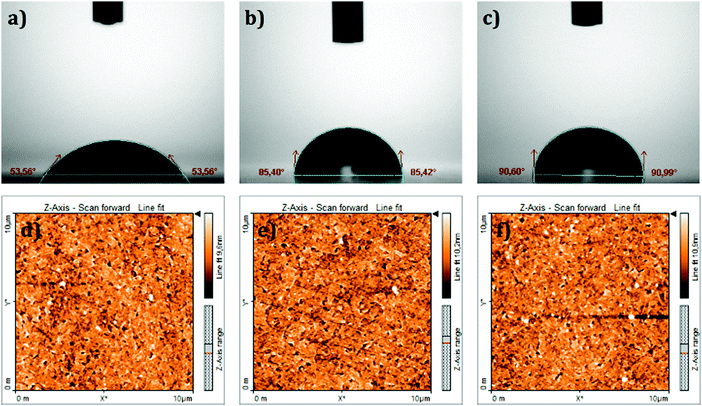 | ||
| Fig. 3 Top: Contact angle measurements on the (a) bare ITO surface, (b) ITO/TPA surface and (c) ITO/MC-43 surface. Bottom: Topographical AFM images of (d) bare ITO, (e) ITO/TPA and (f) ITO/MC-43. | ||
Topographical atomic force microscopy (AFM) images of SAM modified samples were taken to confirm that the SAMs were effectively attached to the ITO surface (see Fig. 3d–f). Root-mean-square (RMS) values of bare ITO, ITO/TPA and ITO/MC-43 are 2.0, 4.5 and 3.5 nm, respectively. Surface roughness values obtained for SAM modified ITO surfaces differ from bare ITO suggesting once again that ITO surfaces are covered by SAM molecules.
The X-ray photoelectron spectroscopy (XPS) was used to determine chemical compositions of modified ITO surfaces coated with MC-43 and TPA molecules. Fig. S13 (ESI†) shows the survey spectrum of C 1s, O 1s and N 1s for ITO/MC-43 and ITO/TPA coatings, respectively. The peaks observed in the survey spectra for MC-43 are for C 1s, O 1s and N 1s with binding energies of 284.08, 529.32 and 398.94 eV, respectively.19,25 Approximately the same results are obtained for TPA. The corresponding binding energies of functional groups for ITO/MC-43 and ITO/TPA are listed as in Table S2 (ESI†). To analyse the atomic bonds formed by carbon and oxygen atoms on the ITO surface after the formation of SAMs, high resolution spectra of C 1s and O 1s were fitted and presented in Fig. 4. The peaks of C 1s for MC-43 on ITO at 284.08, 285.43, and 287.41 eV and for TPA on ITO at 283.95, 284.60 and 287.58 eV are attributed to C–C or C–H, C–O–C and O–C![[double bond, length as m-dash]](https://www.rsc.org/images/entities/char_e001.gif) O, respectively.25 The peaks assigned to ester bonding (O–C
O, respectively.25 The peaks assigned to ester bonding (O–C![[double bond, length as m-dash]](https://www.rsc.org/images/entities/char_e001.gif) O) at 287.41 eV and 287.58 eV indicate the formation of strong covalent bonds between the carboxylic acid (–COOH) head group of MC-43 and TPA SAM molecules and hydroxyl groups (–OH) present on the surface of ITO (Fig. 4a and c).
O) at 287.41 eV and 287.58 eV indicate the formation of strong covalent bonds between the carboxylic acid (–COOH) head group of MC-43 and TPA SAM molecules and hydroxyl groups (–OH) present on the surface of ITO (Fig. 4a and c).
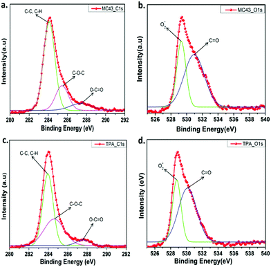 | ||
| Fig. 4 The XPS high resolution survey spectra of C 1s (a) and O 1s (b) for ITO/MC-43. The XPS high resolution survey of C 1s (c) and O 1s (d) for ITO/TPA. | ||
More detailed and fitted high resolution XPS spectra of O 1s for MC-43 and TPA are given in Fig. 4b and d. The peaks observed at 529.32 and 530.96 eV are assigned to the ITO/MC-43 surface and these signals correspond to lattice oxide O2− and C![[double bond, length as m-dash]](https://www.rsc.org/images/entities/char_e001.gif) O groups, respectively. Almost the same peaks are obtained from the ITO/TPA surface with the values of 528.77 and 530.12 eV.19
O groups, respectively. Almost the same peaks are obtained from the ITO/TPA surface with the values of 528.77 and 530.12 eV.19
The XPS measurements were also carried out on bare ITO prior to the deposition of the SAM layers (Fig. S14 in the ESI†). These measurements lack N 1s peaks, which are only present when the nitrogen containing SAM molecules are deposited onto the ITO surface.
Moreover, we recorded the film images (Fig. 5) using scanning electron microscopy (SEM). As can be seen, the use of PEDOT:PSS (Fig. 5b) reveals a more smooth ITO surface where the ITO grains cannot be distinguished. Yet, when the organic molecules are deposited (Fig. 5c and d) the ITO surface is still rough and the nanocrystals can be seen. Nonetheless, much of the nanospace betweel ITO grains is covered. It is feasible that a more rough surface improves the contact between the electrode and the perovskite layer. Furthermore, the molecules at the SAM will provide a favourable dipole moment for efficient charge collection at the ITO electrode.
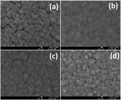 | ||
| Fig. 5 Morphology of the perovskite films on top of the modified or non-modified ITO surface: (a) bare ITO; (b) ITO/PEDOT:PSS; (c) ITO/TPA; and (d) ITO/MC-43. | ||
Solar cell performance
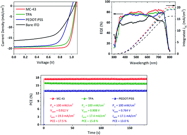
Fig. 2 illustrates the complete device fabrication steps, explained in detail in the Experimental section, in which the perovskite and the fullerene are deposited via spin coating and the final Ag electrode by means of thermal evaporation under high vacuum. As a comparison, we fabricated similar solar cells with exactly the same perovskite composition and thickness with PEDOT:PSS coated ITO instead of SAMs and, alternatively, without any coating (bare ITO sample). The current density–voltage (J–V) characteristics of the best devices are shown in Fig. 6.These measurements were carried out under 1 sun illumination conditions (AM 1.5G, 100 mW cm−2) and performing the voltage scan in the direction VOC to JSC (reverse sweep) at a scan rate of 40 mV s−1. Compared to bare ITO devices, the SAM based cells perform much better especially in terms of FF and JSC, leading to significantly higher PCEs. While the JSC for the PEDOT:PSS device is comparable with the one obtained with SAMs, the FF is below 70% leading to a maximum PCE of 13.0% with an average of 12.3% (see Fig. S7 and Table S1, ESI†, for complete statistics). MC-43 scores a record efficiency of 17.3% with an average of 16.8% while TPA reaches 15.8% as the maximum with an average of 14.6%. The extremely high FF might be related to an optimal formation of the perovskite layer on top of the SAM modified ITO.
All the photovoltaic parameters related to the champion devices are summarized in Table 1. Apart from the bare ITO samples, all cells present negligible or no hysteresis in the J–V (see Fig. S3, ESI†) leading to an excellent consistency of photovoltaic parameters regardless of the scan direction.
| Sample | J SC (mA cm−2) | V OC (V) | FF (%) | η (%) |
|---|---|---|---|---|
| Bare ITO | 16.3 ± 0.2 | 1.05 ± 0.04 | 56.1 ± 0.3 | 9.59 ± 0.3 |
| PEDOT:PSS | 19.2 ± 0.2 | 1.01 ± 0.04 | 67.3 ± 0.3 | 13.0 ± 0.3 |
| TPA | 19.4 ± 0.2 | 1.06 ± 0.04 | 76.9 ± 0.3 | 15.9 ± 0.3 |
| MC-43 | 20.1 ± 0.2 | 1.08 ± 0.04 | 80.0 ± 0.3 | 17.3 ± 0.3 |
As observed by several research groups, and confirmed in this work, the PiN structure based on the MAPI perovskite does not suffer from severe hysteresis issues.26 The external quantum efficiency (EQE) spectra are also shown in Fig. 6. The integrated current density values, plotted on the same graph, match the JSC obtained from the J–V measurements, which for the devices based on TPA and MC-43 is 19.4 and 20.2 mA cm−2 respectively, in excellent agreement with the value obtained from J–V. As it can be seen, the maximum EQE peaks of the top-performing devices can reach over 80% EQE, a notable photon-to-electron conversion for MAPI perovskite solar cells.
The highest FFs reported in the literature are usually due to the utilization of metal cathodes like aluminium or lithium fluoride/aluminium that present better energy alignment for electron extraction. However, despite the difference in energy levels between the LUMO of PC60BM and the work function of Ag, we achieve for all devices very high FF values suggesting efficient charge transfer and extraction. The use of Ag as a top electrode is also preferable for its better stability in order to limit the device degradation and ensure a longer lifetime for the devices. In this context, the performance of the devices has been monitored in a short period, under continuous light illumination, and during several days by performing J–V measurements to evaluate the durability of the devices. In Fig. 6 (bottom), we show the PCE stability under continuous 1 sun equivalent illumination measured by applying the voltage corresponding to the maximum power point, as obtained from the J–V measurement, and registering the given current density. The devices show excellent stability with practically no degradation during the evaluation time. The MC-43 based champion device has been also evaluated in the long-term period. The results are shown in Fig. S5 and S6 (ESI†). After encapsulation, the device still maintains 90% of its efficiency after 20 days of storage in dark and low humidity conditions.
Conclusions
In summary, we have proposed two SAM organic molecules, TPA and MC-43, to be employed as WF modifiers and efficient substitutes of PEDOT:PSS on ITO electrodes. The solar cells fabricated with the planar PiN structure based on our SAMs show remarkable PCE, with the best cell based on TPA scoring 15.9% with a FF of 77%, VOC of 1.06 V and JSC of 19.4 mA cm−2 and the best performing MC-43 cell scoring 17.3% with a FF of 80%, VOC of 1.07 V and JSC of 20.3 mA cm−2.The use of SAMs ensures a homogeneous formation of the MAPI perovskite layer and gives rise to very high FF and VOC. Although ITO/TPA has a 0.2 eV deeper HOMO than ITO/MC-43, the latter shows a slightly higher VOC according to the statistics collected on several devices (see ESI†). An explanation for the best performance of MC-43 based devices is due to its better charge transfer capability (better energy alignment due to its red/ox properties as it is easier to oxidize) when compared to the TPA.
Also it is important to notice that the PCEs obtained with the surface modified MC-43 devices are among the highest values reported in the literature to date. The extremely facile deposition method and the ability of these molecules to form strong covalent bonds with metal oxides and tune their WF, represent a clear benefit to reduce charge losses and ensure contact selectivity. As revealed by our work, these molecules can offer a valid alternative to conventional polymers with the aim of increasing the stability and durability of planar PiN PSCs.
Conflicts of interest
There are no conflicts to declare.Acknowledgements
Dr M. Can gratefully acknowledges the financial support from Council of Higher Education (YÖK) Project-Based Mevlana Exchange Programme (Project Number: MEV-2016-056) and he also acknowledges the supports from Izmir Katip Celebi University Grants Commission (Project Number: 2016-GAP-MUMF-0009). Prof. Palomares thanks ICIQ-BIST and ICREA for their support. Moreover, the Spanish Ministerio de Ciencia, Innovación y Universidades and the Agencia Estatal de Investigación (AEI) are also acknowledged for the CTQ2016800042-R/AIE project and the FPI grant to C. R. S. (BES-2014-068795).References
- A. Kojima, K. Teshima, Y. Shirai and T. Miyasaka, J. Am. Chem. Soc., 2009, 131, 6050–6051 CrossRef CAS PubMed
.
- W. S. Yang, B.-W. Park, E. H. Jung, N. J. Jeon, Y. C. Kim, D. U. Lee, S. S. Shin, J. Seo, E. K. Kim, J. H. Noh and S. I. Seok, Science, 2017, 356, 1376 CrossRef CAS PubMed
.
- Z. Wu, R. Raga Sonia, J. Juarez-Perez Emilio, X. Yao, Y. Jiang, K. Ono Luis, Z. Ning, H. Tian and Y. Qi, Adv. Mater., 2017, 30, 1703670 CrossRef PubMed
.
- S. Pont, D. Bryant, C.-T. Lin, N. Aristidou, S. Wheeler, X. Ma, R. Godin, S. A. Haque and J. R. Durrant, J. Mater. Chem. A, 2017, 5, 9553–9560 RSC
.
- T. Salim, S. Sun, Y. Abe, A. Krishna, A. C. Grimsdale and Y. M. Lam, J. Mater. Chem. A, 2015, 3, 8943–8969 RSC
.
- W. Nie, H. Tsai, R. Asadpour, J.-C. Blancon, A. J. Neukirch, G. Gupta, J. J. Crochet, M. Chhowalla, S. Tretiak, M. A. Alam, H.-L. Wang and A. D. Mohite, Science, 2015, 347, 522 CrossRef CAS PubMed
.
- J. Burschka, N. Pellet, S.-J. Moon, R. Humphry-Baker, P. Gao, M. K. Nazeeruddin and M. Grätzel, Nature, 2013, 499, 316 CrossRef CAS PubMed
.
- Z. Xiao, C. Bi, Y. Shao, Q. Dong, Q. Wang, Y. Yuan, C. Wang, Y. Gao and J. Huang, Energy Environ. Sci., 2014, 7, 2619–2623 RSC
.
- N. J. Jeon, J. H. Noh, Y. C. Kim, W. S. Yang, S. Ryu and S. I. Seok, Nat. Mater., 2014, 13, 897 CrossRef CAS PubMed
.
- E. Eperon Giles, M. Burlakov Victor, P. Docampo, A. Goriely and J. Snaith Henry, Adv. Funct. Mater., 2013, 24, 151–157 CrossRef
.
- Z. Xiao, Q. Dong, C. Bi, Y. Shao, Y. Yuan and J. Huang, Adv. Mater., 2014, 26, 6503–6509 CrossRef CAS PubMed
.
- P. Schulz, E. Edri, S. Kirmayer, G. Hodes, D. Cahen and A. Kahn, Energy Environ. Sci., 2014, 7, 1377–1381 RSC
.
- S. Ameen, A. Rub Malik, A. Kosa Samia, A. Alamry Khalid, M. S. Akhtar, H. Ä. Shin, H. Ä. Seo, M. Asiri Abdullah and K. Nazeeruddin Mohammad, ChemSusChem, 2015, 9, 10–27 CrossRef PubMed
.
- Q. Hu, J. Wu, C. Jiang, T. Liu, X. Que, R. Zhu and Q. Gong, ACS Nano, 2014, 8, 10161–10167 CrossRef CAS PubMed
.
- H. Kim, K.-G. Lim and T.-W. Lee, Energy Environ. Sci., 2016, 9, 12–30 RSC
.
- J. H. Heo, H. J. Han, D. Kim, T. K. Ahn and S. H. Im, Energy Environ. Sci., 2015, 8, 1602–1608 RSC
.
- Y. Bai, H. Chen, S. Xiao, Q. Xue, T. Zhang, Z. Zhu, Q. Li, C. Hu, Y. Yang, Z. Hu, F. Huang, S. Wong Kam, H. Ä. Yip and S. Yang, Adv. Funct. Mater., 2016, 26, 2950–2958 CrossRef CAS
.
- Ç. Kirbiyik, K. Kara, D. A. Kara, M. Z. Yigit, B. Istanbullu, M. Can, N. S. Sariciftci, M. Scharber and M. Kuç, Appl. Surf. Sci., 2017, 423, 521–527 CrossRef
.
- C. Tozlu, A. Mutlu, M. Can, A. K. Havare, S. Demic and S. Icli, Appl. Surf. Sci., 2017, 422, 1129–1138 CrossRef CAS
.
- C.-Y. Chang, Y.-C. Chang, W.-K. Huang, W.-C. Liao, H. Wang, C. Yeh, B.-C. Tsai, Y.-C. Huang and C.-S. Tsao, J. Mater. Chem. A, 2016, 4, 7903–7913 RSC
.
- L. Zuo, Z. Gu, T. Ye, W. Fu, G. Wu, H. Li and H. Chen, J. Am. Chem. Soc., 2015, 137, 2674–2679 CrossRef CAS PubMed
.
- Y. Bai, Q. Dong, Y. Shao, Y. Deng, Q. Wang, L. Shen, D. Wang, W. Wei and J. Huang, Nat. Commun., 2016, 7, 12806 CrossRef CAS PubMed
.
- G. Yang, C. Wang, H. Lei, X. Zheng, P. Qin, L. Xiong, X. Zhao, Y. Yan and G. Fang, J. Mater. Chem. A, 2017, 5, 1658–1666 RSC
.
- E. Yalcin, D. A. Kara, C. Karakaya, M. Z. Yigit, A. K. Havare, M. Can, C. Tozlu, S. Demic, M. Kus and A. Aboulouard, Opt. Mater., 2017, 69, 283–290 CrossRef CAS
.
- P. Prieto, V. Nistor, K. Nouneh, M. Oyama, M. Abd-Lefdil and R. Díaz, Appl. Surf. Sci., 2012, 258, 8807–8813 CrossRef CAS
.
- T. Liu, K. Chen, Q. Hu, R. Zhu and Q. Gong, Adv. Energy Mater., 2016, 6, 1600457 CrossRef
.
Footnote |
| † Electronic supplementary information (ESI) available. See DOI: 10.1039/c8ee01831f |
| This journal is © The Royal Society of Chemistry 2019 |

