 Open Access Article
Realization and direct observation of five normal and parametric modes in silicon nanowire resonators by in situ transmission electron microscopy†
Feng-Chun
Hsia
 abc,
Dai-Ming
Tang
 *a,
Wipakorn
Jevasuwan
a,
Naoki
Fukata
 a,
Xin
Zhou
a,
Masanori
Mitome
a,
Xin
Zhou
a,
Masanori
Mitome
 a,
Yoshio
Bando
 adf,
Torbjörn E. M.
Nordling
 b and
Dmitri
Golberg
 ae
ae
aInternational Center for Materials Nanoarchitectonics (MANA), National Institute for Materials Science (NIMS), 1-1 Namiki, Tsukuba, Ibaraki 305-0044, Japan. E-mail: tang.daiming@nims.go.jp
bDepartment of Mechanical Engineering, National Cheng Kung University, No. 1, University Road, Tainan City 701, Taiwan
cAdvanced Research Center for Nanolithography (ARCNL), Science Park 106, Amsterdam 1098 XG, The Netherlands
dAustralian Institute for Innovative Materials, University of Wollongong, Wollongong, New South Wales 2500, Australia
eSchool of Chemistry, Physics and Mechanical Engineering, Science and Engineering Faculty, Queensland University of Technology (QUT), 2nd George Str., Brisbane, QLD 4000, Australia
fInstitute of Molecular Plus, Tianjin University, No. 11 Building, No. 92 Weijin Road, Nankai District, Tianjin, 300072, P. R. China
First published on 26th February 2019
Abstract
Mechanical resonators have wide applications in sensing bio-chemical substances, and provide an accurate method to measure the intrinsic elastic properties of oscillating materials. A high resonance order with high response frequency and a small resonator mass are critical for enhancing the sensitivity and precision. Here, we report on the realization and direct observation of high-order and high-frequency silicon nanowire (Si NW) resonators. By using an oscillating electric-field for inducing a mechanical resonance of single-crystalline Si NWs inside a transmission electron microscope (TEM), we observed resonance up to the 5th order, for both normal and parametric modes at ∼100 MHz frequencies. The precision of the resonant frequency was enhanced, as the deviation reduced from 3.14% at the 1st order to 0.25% at the 5th order, correlating with the increase of energy dissipation. The elastic modulus of Si NWs was measured to be ∼169 GPa in the [110] direction, and size scaling effects were found to be absent down to the ∼20 nm level.
Introduction
Mechanical resonance is a non-linear response of an oscillating system to specific frequencies linking the external stimuli and the intrinsic microstructure and elastic properties of a material. Resonators are widely used as sensors in micro-/nanoelectromechanical systems (MEMS and NEMS), and are also employed for the elastic property measurements of resonating materials.1–5 While using as mass, chemical and bio-sensors,2–4,6–10 the sensitivity (S) of a resonator is defined by a shift of the resonant frequency with a change of its mass (Δm) calculated as:11,12 | (1) |
Silicon is one of the most important materials for MEMS and NEMS because of the availability of high-quality single crystals and compatibility with microfabrication techniques of the semiconductor industry. One of the most fundamental requirements for application of Si NEMS devices is the elastic properties on the nanometer scale. In previous studies, the Young's modulus of Si NWs was reported in a wide range, from 120 to 170 GPa in the [110] direction21–23 and 60 to 210 GPa in the [111] direction.21,24–31 In addition, there is still controversy over the size scaling effects with respect to Si’s elastic modulus.21,23,27,29 Gordon et al. used a resonance method and reported that the elastic modulus increases with decreasing the NW diameter,27 whereas Calahorra et al. reported the opposite trend under a bending test.21 Such a controversy calls for an accurate measurement of the elastic modulus of Si NWs with direct correlation with their microstructures, such as crystallinity, orientation, diameter and oxide layer thickness.
In this work we investigated the mechanical resonance of individual Si NW cantilevers using an in situ transmission electron microscopy (TEM) approach.31 By carefully tuning the frequency of the oscillating electric field acting on the highly crystallized Si NWs, high-order resonances with high frequencies were realized and visualized up to the 5th order of normal and parametric modes at frequencies of ∼137.5 MHz and ∼68.6 MHz, respectively. The frequencies and their ratios for 10 resonant modes were consistent with the predictions of the classical Euler–Bernoulli (E–B) beam theory. In addition, the precision of the resonant frequency was found to be enhanced for higher resonant mode orders, as the deviations reduced from 3.14% for the 1st order to 0.25% for the 5th order. The converging trend of the resonant frequency is attributed to the higher energy dissipation at higher resonant mode orders, based on the calculation and analysis of the input electric energy and the output mechanical energy from direct observation. We applied these highly sensitive cantilevers to evaluate the elastic moduli of Si NWs and the oxide layer effects. The elastic modulus was found to be consistent with that of bulk Si crystals and the length scaling effects were absent down to the 20 nm level.
Experimental
In situ TEM resonance experimental setup for individual Si NWs
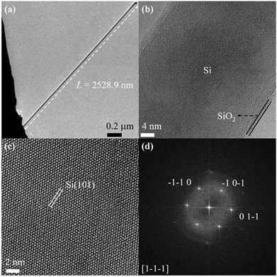
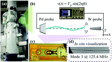
The Si NWs are grown using a vapor–liquid–solid (VLS) approach32 (see also Note S1†). Fig. 1 demonstrates the structural characterization of a typical Si NW by TEM. The length (L) of this Si NW is ∼2529 nm (Fig. 1(a)), which was carefully calibrated by considering the height difference and the TEM magnification, as explained in Note S2.† We used the minimum contrast defocus to estimate the height difference of the two ends. According to the calculated contrast transfer function (CTF), the minimum contrast defocus is about −14 nm. The defocus error should be within 10 nm, and the average error of the length is ∼0.17%, as demonstrated in Note S3.† The circular cross-sectional view of the NW (see Fig. S2†) shows a uniform diameter of ∼23.3 nm and the NW is covered by a naturally formed thin amorphous SiO2 layer (Fig. 1(b)). The high-resolution TEM (HRTEM) image shows that the Si NW has a single-crystalline structure and presents clearly resolved lattice fringes of Si (101) planes (Fig. 1(c)). The corresponding fast Fourier transform (FTT) pattern (Fig. 1(d)) is indexed as the Si [1−1−1] zone axis, with the NW growth direction along the [101] orientation.The mechanical vibration of a Si NW is induced by an oscillating electric field between the Si NW and a W probe (see probe preparation in Note S4†) in a JEOL-3100F TEM shown in Fig. 2, as explained in Note S5.† Based on the Euler–Bernoulli (E–B) beam theory, the equation of motion for a uniform circular cross-sectional NW is derived as:33
 | (2) |
 | (3) |
![[thin space (1/6-em)]](https://www.rsc.org/images/entities/char_2009.gif) βiL·cosh
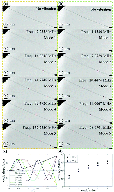
βiL·cosh![[thin space (1/6-em)]](https://www.rsc.org/images/entities/char_2009.gif) βiL = −1, with eigenvalues β1 = 1.87, β2 = 4.69, β3 = 7.85, β4 = 10.99 and βi ≈ (2i − 1)π/2 for i ≥ 5. In addition to the normal mode resonance, parametric modes could be found at frequencies 2fi/n for the nth parametric modes, by solving eqn (2) with a non-zero periodic force, as explained in Note S6.†
βiL = −1, with eigenvalues β1 = 1.87, β2 = 4.69, β3 = 7.85, β4 = 10.99 and βi ≈ (2i − 1)π/2 for i ≥ 5. In addition to the normal mode resonance, parametric modes could be found at frequencies 2fi/n for the nth parametric modes, by solving eqn (2) with a non-zero periodic force, as explained in Note S6.†
Results and discussion
Realization and observation of five normal and parametric resonances
In order to measure the resonant frequency at different mode orders, we first swept the driving frequency within a certain frequency range, as predicted by eqn (3) from the NW’s dimensions. Then, we finely tuned the driving frequency to induce the largest vibration amplitude to locate the resonant frequency. Under careful tuning, we were able to realize and observe up to 10 resonant mode orders for one Si NW. Fig. 3(a) and Video S1† demonstrate the in situ recorded mechanical resonant motions, from the 1st order to the 5th order, at the resonant frequencies of ∼2.2 MHz, ∼14.9 MHz, ∼41.8 MHz, ∼82.5 MHz and ∼137.5 MHz. Another series of resonant frequencies, from the 1st order to the 5th order (Fig. 3(b)), were recorded and could be denoted as the parametric resonance. The relation between normal and parametric resonances can be derived by the Mathieu equation (see eqn S(3)†). In the Strutt diagram34 (see Fig. S4†), the orange shaded area illustrates the instability regions, where the parametric resonance can be excited, as described in Note S6,† with the resonant frequency written as:34–36 | (4) |
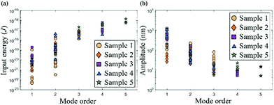
It is noticed that the lower resonance orders could be excited in a wider frequency range compared to the higher orders. For example, for the 1st order, a 10 kHz sweeping step can easily locate the resonance. However, for the 5th order, the step needs to be 100 Hz, which is ∼1 ppm of a resonant frequency of ∼100 MHz. Such a converging trend for the resonance conditions could be understood from the analysis of the input, output and dissipated energies. In previous studies, energy dissipation has been attributed to environmental factors, such as viscosity, temperature, clamping loss, intrinsic defects, and the change of the elastic energy.11,15,16,37–42 Here, we take advantage of the in situ technique to directly measure and calculate the input and output energies. The input energy can be assumed as the energy of a capacitor, between the free end of the Si NW and the W probe.30,43 The energy stored in the capacitor (Wc) is expressed as:
 | (5) |
Evaluation of the Si NW’s modulus and absence of size-effects
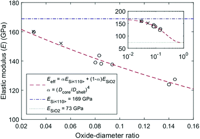
The strict resonant requirement at high-order modes provides an opportunity to precisely evaluate the elastic modulus of Si NWs. By calculations from eqn (3) using the frequencies of the 2nd resonance order, it is found that the effective modulus of the NW is in the range between ∼124 GPa and ∼160 GPa (Fig. 5), depending on the thickness of the oxide layer. The HRTEM image (Fig. 1(c)) reveals that the Si NW grows along the [110] direction and its surface is covered by a thin SiO2 layer. Therefore, the Si NW can be modelled as a core–shell structure, where the bulk Si〈110〉 NW serves as the core and the SiO2 layer as the shell. The elastic modulus of the core–shell structure (Ecs) can be calculated using the flexural rigidity model:27| Ecs = αEcore + (1 − α)Eshell | (6) |
 | (7) |
To be noticed, a nanoparticle has been observed attached on the free-end of the Si NW (Fig. 1(a)). The nanoparticle is the gold particle used as the catalyst in VLS growth, which can be considered as an added mass to cause a shift in the resonant frequency of ∼2%; and an error in the Eeff of ∼0.77%, as calculated in Note S11.† Here, we defined an oxide–diameter ratio as the thickness of the SiO2 layer divided by the diameter (D) of the Si NW. The model predicts an oxide–diameter ratio ranging from ∼0.02 to ∼0.15 (Fig. 5), and offers a full range simulation (Fig. 5 inset) under the combination of ESi〈110〉 (∼169 GPa),44ESiO2 (∼73 GPa)45 and α. Comparing the experimental data of the 2nd order with the flexural rigidity model (Fig. 5), the coefficient of determination (R2) is 0.97, which indicates that the model provides a reliable description of the experimental data for a diameter (Dcore) ranging from ∼19 nm to ∼33 nm. Importantly, the Si NW displays no size-effects within this diameter range, and the modulus is consistent with that of the bulk crystals, confirming the validity of the classical continuum mechanics at the NW sizes down to ∼20 nm.
Elasticity and size-effects of Si NWs have been intensively investigated, and controversial results have been reported, and the feasibility of continuum mechanics is also controversial.21,23,29,46 For example, Zhu et al. applied tensile tests to measure the mechanical properties of Si NWs and demonstrated that the Young's modulus decreases upon reducing the size of the NWs.23 There are two models, one is the continuum model on the macroscale and the other is the atomic model. In the continuum system, the NW is considered as a homogeneous and linear elastic material; in the atomic model, the nature of the individual bonding interactions presents the mechanical properties of an oscillating chain of atoms. According to the literature,47,48 molecular dynamics (MD) simulations and first principles calculations were used to simulate the elastic modulus of the Si NWs. Surface effects, such as surface elasticity and bonding on the NW’s surface, have been addressed as the main factors of size-effects. The surface area to volume ratio (RS) is a parameter used to evaluate size-effects (RS = 4a/D where a is the interatomic distance, approximately 0.2 nm). Numerical results show that when RS is smaller than ∼8%,48 the surface effects show minor contribution to the elastic modulus. In our work, RS is estimated to be ∼4%, with the smallest diameter being ∼20 nm. In addition, the surface of the Si NWs is covered by an oxide layer, which saturates the dangling bonds of the Si surface. Because of the small proportion of surface atoms and surface saturation it is reasonable that size-effects are absent down to the 20 nm level. We have analysed the different size scaling behaviours from three aspects, by comparing our work with Zhu et al.'s paper23 as an example. First, different experimental methods have been used. We used the resonance method and previous work used the tensile elongation method. Second, different models have been considered. We have considered the effect of the surface oxide layer by using a core–shell model, instead of the oxide layer-free model in previous work. Third, the size range is different. The size related softening effects were reported to be strong in the sub-20 nm region, and the minimum diameter in our work is ∼20 nm.
Comparison of resonant frequency and mode orders of Si resonators
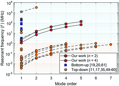
As discussed in the Introduction, the sensitivity of mechanical resonators is related to the resonant frequency, mode order and oscillator’s mass. Fig. 6 presents a plot of the resonant frequency and the mode order of micro/nano-Si resonators fabricated using a top-down approach11,17,35,49–60 compared to nano-Si resonators made using a bottom-up approach.19,20,61 Generally, top-down Si micro/nano-resonators can demonstrate very high resonant mode orders at low frequencies due to the micrometer size.11,17,52,59 To enhance the frequency and reduce the mass of the resonators, NW resonators have been intensively investigated during the past two decades. Indeed, very high frequency resonators, at approximately 200 MHz, have been demonstrated.19 However, up to now, only the 1st and the 2nd orders of normal mode resonances have been realized in NW resonators.20 By contrast, in the current work, the full potential of Si NW resonators has been demonstrated by in situ TEM measurements and direct observations. Normal and parametric resonances up to the 5th order were realized and directly observed at frequencies of ∼100 MHz level.Conclusions
By using an in situ TEM method, we realized and directly observed both normal and parametric modes of Si NW resonators, up to the 5th order, at the resonant frequencies of ∼100 MHz. The frequencies and ratios of different mode orders and parametric resonances were consistent with the prediction of the classical Euler–Bernoulli beam theory and the parametric resonance derived by the Mathieu equation, implying that the continuum model is valid down to the nanometer scale. The resonating ranges demonstrated a converging trend with increasing mode orders and resonant frequencies, implying the potential applications for precise sensors at high-order resonant modes. The elastic moduli of the Si NWs have been accurately evaluated, and no size-effects were found for the NW diameter down to 20 nm.Conflicts of interest
There are no conflicts to declare.Acknowledgements
The work was supported by JSPS Kakenhi Grant 25820336, the Transmission Electron Microscopy Station, World Premier International (WPI) Center for Materials Nanoarchitectonics (MANA), National Institute for Materials Science (NIMS), Japan, National Cheng Kung University (NCKU), Ministry of Science and Technology of Taiwan (MOST-105-2218-E-006-016-MY2 and MOST-107-2634-F-006-009), and MOST AI Biomedical Research Center at NCKU. F.-C. H. acknowledges the scholarships from the NIMS internship program and Global Networking Talent 3.0 Plan – Biomedical Engineering sponsored by the Medical Device Innovation Center at NCKU and the Ministry of Education, Taiwan. D. G. is grateful to the Australian Research Council (ARC) for granting a Laureate Fellowship FL160100089 and QUT Project No. 322170-0355/51.Notes and references
- J. S. Bunch, A. M. van der Zande, S. S. Verbridge, I. W. Frank, D. M. Tanenbaum, J. M. Parpia, H. G. Craighead and P. L. McEuen, Science, 2007, 315, 490–493 CrossRef CAS PubMed.
- Resonant MEMS, ed. O.Brand, I.Dufour, S. M.Heinrich and F.Josse, Wiley-VCH Verlag GmbH & Co. KGaA, Weinheim, Germany, 2015 Search PubMed.
- K. L. Ekinci and M. L. Roukes, Rev. Sci. Instrum., 2005, 76, 061101 CrossRef.
- H. G. Craighead, Science, 2000, 290, 1532–1535 CrossRef CAS PubMed.
- K. Jensen, J. Weldon, H. Garcia and A. Zettl, Nano Lett., 2007, 7, 3508–3511 CrossRef CAS PubMed.
- T. P. Burg, M. Godin, S. M. Knudsen, W. Shen, G. Carlson, J. S. Foster, K. Babcock and S. R. Manalis, Nature, 2007, 446, 1066–1069 CrossRef CAS PubMed.
- M. Calleja, M. Nordström, M. Álvarez, J. Tamayo, L. M. Lechuga and A. Boisen, Ultramicroscopy, 2005, 105, 215–222 CrossRef CAS PubMed.
- K. Jensen, K. Kim and A. Zettl, Nat. Nanotechnol., 2008, 3, 533–537 CrossRef CAS PubMed.
- P. Poncharal, Science, 1999, 283, 1513–1516 CrossRef CAS PubMed.
- Y. T. Yang, C. Callegari, X. L. Feng, K. L. Ekinci and M. L. Roukes, Nano Lett., 2006, 6, 583–586 CrossRef CAS PubMed.
- M. K. Ghatkesar, V. Barwich, T. Braun, J.-P. Ramseyer, C. Gerber, M. Hegner, H. P. Lang, U. Drechsler and M. Despont, Nanotechnology, 2007, 18, 445502 CrossRef.
- T. Braun, V. Barwich, M. K. Ghatkesar, A. H. Bredekamp, C. Gerber, M. Hegner and H. P. Lang, Phys. Rev. E: Stat., Nonlinear, Soft Matter Phys., 2005, 72, 031907 CrossRef PubMed.
- C. A. Van Eysden and J. E. Sader, J. Appl. Phys., 2007, 101, 044908 CrossRef.
- L. B. Biedermann, R. C. Tung, A. Raman, R. G. Reifenberger, M. M. Yazdanpanah and R. W. Cohn, Nanotechnology, 2010, 21, 305701 CrossRef PubMed.
- J. H. Ko, J. Jeong, J. Choi and M. Cho, Appl. Phys. Lett., 2011, 98, 171909 CrossRef.
- J. E. Sader, J. Lee and S. R. Manalis, J. Appl. Phys., 2010, 108, 114507 CrossRef PubMed.
- J. P. Killgore and D. C. Hurley, Nanotechnology, 2012, 23, 055702 CrossRef PubMed.
- Y. Jia, S. Du, E. Arroyo and A. A. Seshia, Appl. Phys. Lett., 2018, 112, 171901 CrossRef.
- X. L. Feng, R. He, P. Yang and M. L. Roukes, Nano Lett., 2007, 7, 1953–1959 CrossRef CAS.
- O. Malvar, E. Gil-Santos, J. J. Ruz, D. Ramos, V. Pini, M. Fernandez-Regulez, M. Calleja, J. Tamayo and A. San Paulo, Appl. Phys. Lett., 2013, 103, 033101 CrossRef.
- Y. Calahorra, O. Shtempluck, V. Kotchetkov and Y. E. Yaish, Nano Lett., 2015, 15, 2945–2950 CrossRef CAS PubMed.
- H. Zhang, J. Tersoff, S. Xu, H. Chen, Q. Zhang, K. Zhang, Y. Yang, C.-S. Lee, K.-N. Tu, J. Li and Y. Lu, Sci. Adv., 2016, 2, e1501382 CrossRef PubMed.
- Y. Zhu, F. Xu, Q. Qin, W. Y. Fung and W. Lu, Nano Lett., 2009, 9, 3934–3939 CrossRef CAS PubMed.
- C.-L. Hsin, W. Mai, Y. Gu, Y. Gao, C.-T. Huang, Y. Liu, L.-J. Chen and Z.-L. Wang, Adv. Mater., 2008, 20, 3919–3923 CrossRef CAS.
- K. Zhang, Q. Zhu and Z. Chen, Sensors, 2017, 17, 1621 CrossRef PubMed.
- A. San Paulo, J. Bokor, R. T. Howe, R. He, P. Yang, D. Gao, C. Carraro and R. Maboudian, Appl. Phys. Lett., 2005, 87, 053111 CrossRef.
- M. J. Gordon, T. Baron, F. Dhalluin, P. Gentile and P. Ferret, Nano Lett., 2009, 9, 525–529 CrossRef CAS PubMed.
- M. Tabib-Azar, M. Nassirou, R. Wang, S. Sharma, T. I. Kamins, M. S. Islam and R. S. Williams, Appl. Phys. Lett., 2005, 87, 113102 CrossRef.
- Y.-S. Sohn, J. Park, G. Yoon, J. Song, S.-W. Jee, J.-H. Lee, S. Na, T. Kwon and K. Eom, Nanoscale Res. Lett., 2010, 5, 211–216 CrossRef CAS PubMed.
- D. Garcia-Sanchez, A. San Paulo, M. J. Esplandiu, F. Perez-Murano, L. Forró, A. Aguasca and A. Bachtold, Phys. Rev. Lett., 2007, 99, 085501 CrossRef CAS PubMed.
- D.-M. Tang, C.-L. Ren, M.-S. Wang, X. Wei, N. Kawamoto, C. Liu, Y. Bando, M. Mitome, N. Fukata and D. Golberg, Nano Lett., 2012, 12, 1898–1904 CrossRef CAS PubMed.
- N. Fukata, M. Mitome, T. Sekiguchi, Y. Bando, M. Kirkham, J.-I. Hong, Z. L. Wang and R. L. Snyder, ACS Nano, 2012, 6, 8887–8895 CrossRef CAS PubMed.
- S. S. Rao and F. F. Yap, Mechanical Vibrations, Prentice Hall UpperSaddle River, 2011, vol. 4 Search PubMed.
- A. H. Nayfeh and D. T. Mook, Nonlinear Oscillations, John Wiley & Sons, 2008 Search PubMed.
- K. L. Turner, S. A. Miller, P. G. Hartwell, N. C. MacDonald, S. H. Strogatz and S. G. Adams, Nature, 1998, 396, 149–152 CrossRef CAS.
- M.-F. Yu, G. J. Wagner, R. S. Ruoff and M. J. Dyer, Phys. Rev. B: Condens. Matter Mater. Phys., 2002, 66, 073406 CrossRef.
- S. S. Verbridge, D. F. Shapiro, H. G. Craighead and J. M. Parpia, Nano Lett., 2007, 7, 1728–1735 CrossRef CAS PubMed.
- T. P. Burg, J. E. Sader and S. R. Manalis, Phys. Rev. Lett., 2009, 102, 228103 CrossRef PubMed.
- D. A. Harrington, P. Mohanty and M. L. Roukes, Phys. B, 2000, 284–288, 2145–2146 CrossRef CAS.
- S. Schmid and C. Hierold, J. Appl. Phys., 2008, 104, 093516 CrossRef.
- Q. P. Unterreithmeier, T. Faust and J. P. Kotthaus, Phys. Rev. Lett., 2010, 105, 027205 CrossRef PubMed.
- M. Imboden and P. Mohanty, Phys. Rep., 2014, 534, 89–146 CrossRef.
- S. Perisanu, V. Gouttenoire, P. Vincent, A. Ayari, M. Choueib, M. Bechelany, D. Cornu and S. T. Purcell, Phys. Rev. B, 2008, 77, 165434 CrossRef.
- M. A. Hopcroft, W. D. Nix and T. W. Kenny, J. Microelectromech. Syst., 2010, 19, 229–238 CAS.
- H. Ni, X. Li and H. Gao, Appl. Phys. Lett., 2006, 88, 043108 CrossRef.
- M. J. Gordon, T. Baron, F. Dhalluin, P. Gentile and P. Ferret, Nano Lett., 2009, 9, 525–529 CrossRef CAS PubMed.
- H. N. Pishkenari, B. Afsharmanesh and E. Akbari, Curr. Appl. Phys., 2015, 15, 1389–1396 CrossRef.
- R. E. Rudd and B. Lee, Mol. Simul., 2008, 34, 1–8 CrossRef CAS.
- A. Labuda, M. Kocun, M. Lysy, T. Walsh, J. Meinhold, T. Proksch, W. Meinhold, C. Anderson and R. Proksch, Rev. Sci. Instrum., 2016, 87, 073705 CrossRef PubMed.
- W. C. Jiang, X. Lu, J. Zhang and Q. Lin, Opt. Express, 2012, 20, 15991 CrossRef CAS PubMed.
- J. Yang, T. Ono and M. Esashi, J. Microelectromech. Syst., 2002, 11, 775–783 CrossRef CAS.
- R. S. Gates, W. A. Osborn and J. R. Pratt, Nanotechnology, 2013, 24, 255706 CrossRef PubMed.
- I. Bargatin, E. B. Myers, J. S. Aldridge, C. Marcoux, P. Brianceau, L. Duraffourg, E. Colinet, S. Hentz, P. Andreucci and M. L. Roukes, Nano Lett., 2012, 12, 1269–1274 CrossRef CAS PubMed.
- D. W. Carr, S. Evoy, L. Sekaric, H. G. Craighead and J. M. Parpia, Appl. Phys. Lett., 1999, 75, 920–922 CrossRef CAS.
- M. Nasr Esfahani, Y. Kilinc, M. Çagatay Karakan, E. Orhan, M. S. Hanay, Y. Leblebici and B. Erdem Alaca, J. Micromech. Microeng., 2018, 28, 045006 CrossRef.
- A. Koumela, D. Mercier, V. Gouttenoire, C. Marcoux, S. T. Purcell and L. Duraffourg, Procedia Eng., 2011, 25, 1649–1652 CrossRef CAS.
- X. Li, T. Ono, Y. Wang and M. Esashi, Appl. Phys. Lett., 2003, 83, 3081–3083 CrossRef CAS.
- T. Tsushima, Y. Asahi, H. Tanigawa, T. Furutsuka and K. Suzuki, Jpn. J. Appl. Phys., 2018, 57, 067201 CrossRef.
- T. Ikehara, J. Lu, M. Konno, R. Maeda and T. Mihara, J. Micromech. Microeng., 2007, 17, 2491–2494 CrossRef.
- M. Li, W. H. P. Pernice and H. X. Tang, Nat. Nanotechnol., 2009, 4, 377–382 CrossRef CAS PubMed.
- R. He, X. L. Feng, M. L. Roukes and P. Yang, Nano Lett., 2008, 8, 1756–1761 CrossRef PubMed.
Footnote |
| † Electronic supplementary information (ESI) available. See DOI: 10.1039/c8na00373d |
| This journal is © The Royal Society of Chemistry 2019 |

