
 Open Access Article
 This Open Access Article is licensed under a
 Creative Commons Attribution 3.0 Unported Licence
Epitaxial highly ordered Sb:SnO2 nanowires grown by the vapor liquid solid mechanism on m-, r- and a-Al2O3†
M.
Zervos
 *a,
N.
Lathiotakis
b,
N.
Kelaidis
c,
A.
Othonos
d,
E.
Tanasa
e and
E.
Vasile
e
*a,
N.
Lathiotakis
b,
N.
Kelaidis
c,
A.
Othonos
d,
E.
Tanasa
e and
E.
Vasile
e
aNanostructured Materials and Devices Laboratory, School of Engineering, University of Cyprus, PO Box 20537, Nicosia, 1678, Cyprus. E-mail: zervos@ucy.ac.cy
bTheoretical and Physical Chemistry Institute, National Hellenic Research Foundation, Vass. Constantinou 48, GR-11635 Athens, Greece
cFaculty of Engineering, Environment and Computing, Coventry University, Priory Street, Coventry CV1 5FB, UK
dLaboratory of Ultrafast Science, Department of Physics, University of Cyprus, P.O. Box 20537, Nicosia, 1678, Cyprus
eDepartment of Science and Engineering of Oxide Materials and Nanomaterials, Politehnica University of Bucharest, 313 Splaiul Independentei, Bucharest, 060042, Romania
First published on 9th April 2019
Abstract
Epitaxial, highly ordered Sb:SnO2 nanowires were grown by the vapor–liquid–solid mechanism on m-, r- and a-Al2O3 between 700 °C and 1000 °C using metallic Sn and Sb with a mass ratio of Sn/Sb = 0.15 ± 0.05 under a flow of Ar and O2 at 1 ± 0.5 mbar. We find that effective doping and ordering can only be achieved inside this narrow window of growth conditions. The Sb:SnO2 nanowires have the tetragonal rutile crystal structure and are inclined along two mutually perpendicular directions forming a rectangular mesh on m-Al2O3 while those on r-Al2O3 are oriented in one direction. The growth directions do not change by varying the growth temperature between 700 °C and 1000 °C but the carrier density decreased from 8 × 1019 cm−3 to 4 × 1017 cm−3 due to the re-evaporation and limited incorporation of Sb donor impurities in SnO2. The Sb:SnO2 nanowires on r-Al2O3 had an optical transmission of 80% above 800 nm and displayed very long photoluminescence lifetimes of 0.2 ms at 300 K. We show that selective area location growth of highly ordered Sb:SnO2 nanowires is possible by patterning the catalyst which is important for the realization of novel nanoscale devices such as nanowire solar cells.
1 Introduction
Metal oxide semiconductor nanowires (NWs) such as Sb:SnO2,1 Sn:In2O3,2 Al:ZnO3 and In:ZnO4 NWs have a high conductivity but they are also capable of light emission as shown for Sn:In2O3 NWs by O' Dwyer et al.5 and Gao et al.6 Despite ongoing efforts into the growth and properties of such metal oxide (MO) NWs only a few have obtained epitaxial, ordered networks which is essential for the realization of novel nanoscale devices with improved performance like nanowire solar cells (NWSCs). More specifically Wan et al.7 has obtained ordered Sn :In2O3 NWs by homo epitaxy on an Sn:In2O3 buffer layer while Nguyen et al.8 and Gao et al.6 have obtained ordered Sn:In2O3 NWs by hetero epitaxy on m-, a- and c-Al2O3. To the best of our knowledge all other MO NWs that have been obtained previously are not oriented in an epitaxial fashion along any particular direction. It is important then to obtain earth abundant MO NWs such as Sb:SnO2 NWs as low cost alternatives to Sn:In2O3.In the past we have grown SnO2 NWs via the vapor liquid solid (VLS) mechanism at 800 °C and 10−1 mbar which had a carrier density of the order of 1016 cm−3 and mobility of 70 cm2 V−1 s−1, as determined from THz conductivity spectroscopy.9 High conductivity SnO2 NWs have been obtained via the incorporation of Sb,10 Mo11 and F12 in SnO2 NWs, while recently, Ma et al.13 showed theoretically that a semiconductor to semimetal transition is possible via the incorporation of Pb in SnO2. However, in most cases Sb has been used as an n-type donor impurity in SnO2 NWs.14–24 All of the Sb:SnO2 NWs have been obtained by using metallic Sn and Sb in the past, but they were not ordered.
Nevertheless, it is necessary to point out that Mathur et al.25 has obtained un-doped SnO2 NWs via the VLS mechanism that were ordered on TiO2 (001) which is isostructural with the tetragonal rutile crystal structure of SnO2. Similarly, Kim et al.26 obtained un-doped, epitaxial, SnO2 NWs on TiO2 (101) while Leonardy et al.27 investigated the structural properties of ordered, un-doped, SnO2 NWs on m- and a-Al2O3 at 700 °C by using SnO under a flow of Ar at 10 mbar. Both Mathur et al.25 and Leonardy et al.27 obtained SnO2 NWs which were oriented in two mutually perpendicular directions while the SnO2 NWs of Kim et al.26 were aligned in three directions. Others like Mazeina et al.28 have grown vertical, un-doped SnO2 NWs via the VLS mechanism on c-Al2O3 at 900 °C with limited ordering and uniformity. Lateral, but un-doped SnO2 NWs have also been obtained by Kim et al.29 and Choi et al.30 while more recently Wang et al.31 investigated lateral SnO2 NWs that were aligned on the surface of m-Al2O3. All of these studies on epitaxial, ordered un-doped SnO2 NWs25–30 focused primarily on their growth and structural properties. It is imperative then to investigate the electrical and optical properties of similar Sb:SnO2 NWs which is critical in evaluating their potential for subsequent use in devices such as NWSCs.
Here we show that epitaxial, ordered Sb:SnO2 NWs can be grown via the VLS mechanism on m-, r- and a- oriented Al2O3 only in a narrow window of growth conditions. We describe their morphology, structural, electrical and optical properties, in detail and show that selective area location growth of ordered Sb:SnO2 NWs is possible which in turn is attractive for the realization of NWSCs as a low cost alternative to Sn:In2O3 NWs.
2 Methods
2.1. Epitaxial growth of Sb:SnO2 NWs
The Sb:SnO2 NWs were grown using a 1′′ hot wall, low pressure chemical vapour deposition (LPCVD) reactor, capable of reaching 1100 °C, which was fed via a micro flow leak valve positioned on the upstream side, just after the gas manifold which consists of four mass flow controllers. A chemically resistant, rotary pump that can reach 10−4 mbar was connected downstream. For the growth of the Sb:SnO2 NWs, metallic Sn and Sb (Aldrich, 100 Mesh, 99.9%) were weighed with an accuracy of ±1 mg. We used an excess of Sb, i.e. a mass ratio of Sn/Sb ≈ 0.1, and the total mass of Sb and Sn was kept fixed and equal to 100 mg or 0.1 g. Square samples of 10 mm × 10 mm c-, m-, r- and a-Al2O3 were cleaned sequentially in trichloroethylene, methanol, acetone, isopropanol, rinsed with de-ionised water, dried with nitrogen and then coated with ≈1 nm Au. The elemental Sb and Sn as well as the c-, m-, r- or a-Al2O3 substrates were loaded in the same quartz boat which was positioned at the centre of the 1′′ LPCVD reactor. The latter was pumped down to 10−4 mbar and purged with 1000 sccm of Ar for 10 min at 1 mbar. Subsequently the temperature was ramped up to 800 °C at 30°C min−1 using the same flow of Ar. Upon reaching 800 °C a flow of 10 sccm O2 was added to the flow of Ar in order to grow the Sb:SnO2 NWs over 10 min at 1 mbar, followed by cool down without O2. We have grown Sb:SnO2 NWs on c-, m-, r- and a-Al2O3 using these growth conditions and changed the growth temperature between 700 °C to 1000 °C.2.2. Characterization of Sb:SnO2 NWs
The morphology, crystal structure and composition of the Sb:SnO2 NWs was determined by scanning electron microscopy (SEM), X-ray diffraction (XRD) and Energy Dispersive X-ray analysis (EDX). High resolution transmission electron microscopy (HRTEM) was carried out using a TECNAI F30 G2 S-TWIN operated at 300 kV. The optical properties of the Sb:SnO2 NWs were determined by steady state and transient absorption–transmission spectroscopy. The steady state and time resolved photoluminescence (PL) were also measured between 10 K and 300 K, while the electrical properties, i.e. carrier density and resistivity, were measured by the Hall effect in the Van der Pauw geometry similar to Costa et al.23,24 In particular the Sb:SnO2 NWs were transferred from the m-, r- or a-Al2O3 onto 10 mm × 10 mm c-Al2O3 by applying pressure. This results into a dry transfer of the ordered Sb:SnO2 NWs onto the c-Al2O3 and the formation of a planar interconnected network. We then deposited In contacts over the Sb:SnO2 NWs by thermal evaporation using a shadow mask. The Sb:SnO2 NWs on c-Al2O3 was not heated up during the deposition, and the In contacts had diameters of ≈1 mm at the four corners of the 10 mm × 10 mm c-Al2O3, but we did not anneal them. The Hall effect was measured using a GMW3470 Electromagnet at 0.3 Tesla. The magnetic field was calibrated with a Hirst GM08 Gaussmeter. A Keithley 2635 A current source and Keithley 2182A nano-voltmeter, controlled by Lab View were used to provide a current and measure the voltages.3 Results and discussion
In the past, we have shown that the reaction of Sn with O2 at 800 °C and 10−1 mbar results into a high yield and uniform distribution of SnO2 NWs on Si (001) or fused SiO2. The SnO2 NWs have average diameters of ≈50 nm, lengths up to ≈100 μm and grow by the VLS mechanism whereby Sn enters the Au catalyst particles on the surface of Si (001) or fused SiO2 and forms liquid Au:Sn particles. Upon saturation, solid SnO2 forms beneath the liquid Au:Sn particles via the reaction with O2 at the triple phase junction, as shown in Fig. 1(a), leading to one dimensional, bottom-up growth.32 However, the SnO2 NWs obtained on Si (001) or fused SiO2 were not oriented or ordered along any direction, and had a carrier density of the order of 1016 cm−3 with a mobility of 70 cm2 V−1 s−1, as determined from THz conductivity spectroscopy.33 Hence doping is required to increase their conductivity. Recently, we showed that higher carrier densities of the order of 1018 to 1019 cm−3 may be readily obtained in Sb doped SnO2 NWs grown on both Si (001) and fused SiO2.34 We obtained a high carrier density of 4 × 1019 cm−3 in the Sb:SnO2 NWs grown on c-Al2O3 at 800 °C and 1 mbar by adding metallic Sb to Sn but the Sb:SnO2 NWs were not ordered or oriented in any particular direction, similar to those obtained previously on Si (001) and fused SiO2.34 This is in contrast to the findings of Mazeina et al.,28 who obtained vertical but un-doped SnO2 NWs via the VLS mechanism on c-Al2O3 at 900 °C with a limited degree of ordering and uniformity. Similarly, we did not obtain ordered Sb:SnO2 NWs on c-Al2O3 by changing the growth temperature between 800 °C and 1000 °C. The epitaxial growth and ordering of Sb:SnO2 NWs on c-Al2O3 is not favorable in view of the fact that SnO2 has a tetragonal crystal structure which will not match the hexagonal crystal structure of the underlying c-Al2O3. However, we observed the formation of ordered Sb:SnO2 NWs on the sides of the c-Al2O3, as described in more detail in the ESI,† which is related to its specific crystallographic orientation. Therefore we carried out the growth of the Sb:SnO2 NWs on m- , r- and a-Al2O3 at 800 °C and 1 mbar using the same growth conditions described above.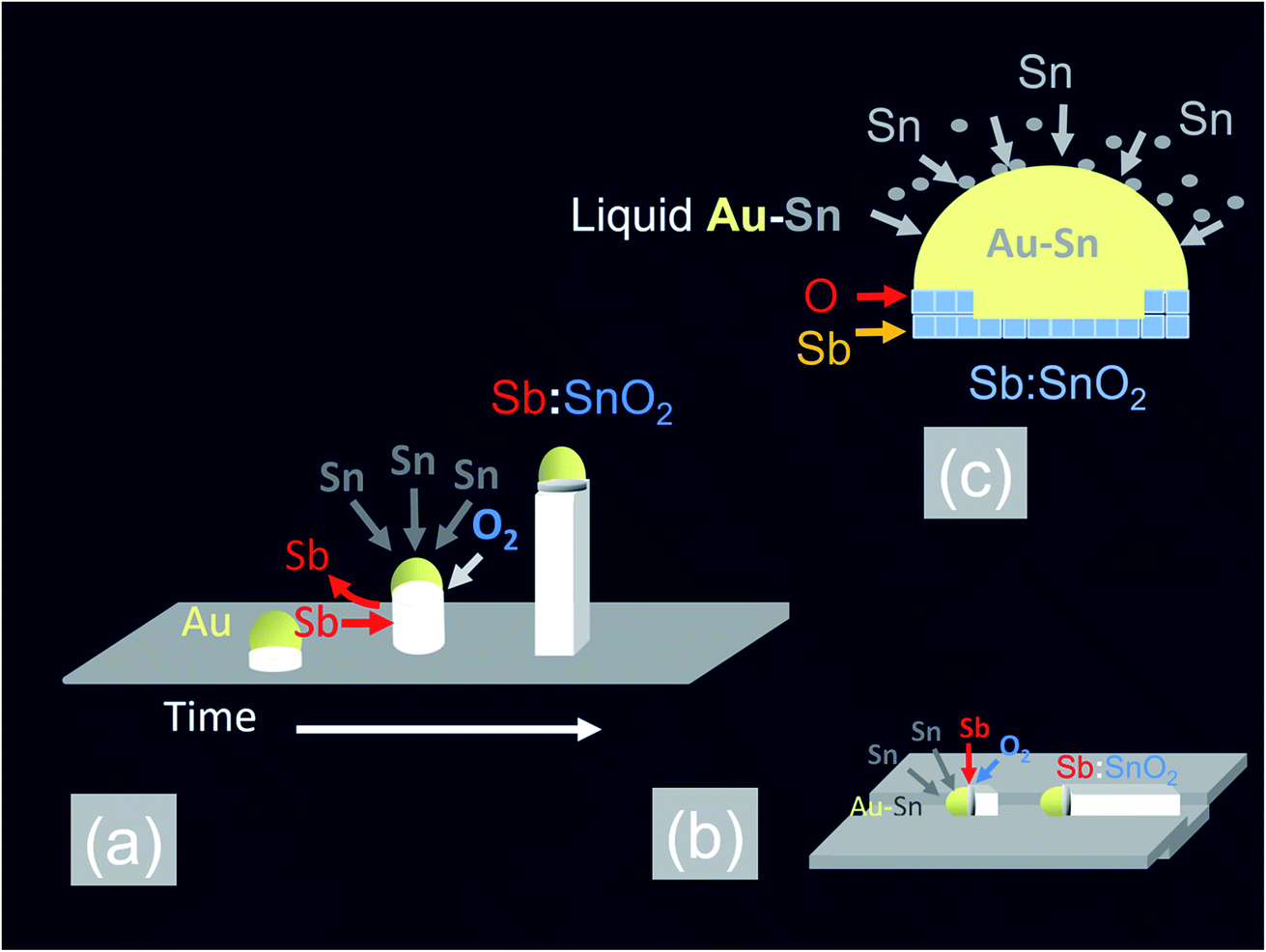 | ||
| Fig. 1 Schematic representation of the VLS growth mechanism of Sb:SnO2 NWs (a) bottom-up growth (b) lateral growth along a step or groove (c) Sb donor impurity incorporation mechanism. | ||
3.1 Growth of Sb:SnO2 NWs on m-, r- and a-Al2O3
We readily obtained ordered Sb:SnO2 NWs on all three surfaces i.e. m-, r- and a-Al2O3, as shown in Fig. 2, 3 and 4 respectively. The Sb:SnO2 NWs on m-Al2O3 are aligned along two mutually perpendicular directions as shown by the SEM images in Fig. 2(a and b), but are inclined with respect to the surface, similar to the SnO2 NWs obtained by Mathur et al.25 and Leonardy et al.27 In contrast, the Sb:SnO2 NWs on r-Al2O3 are all oriented along one direction as shown in Fig. 3(a)–(c). However, upon closer inspection we find that the Sb:SnO2 NWs on r-Al2O3 consist of two segments. The first segment is inclined at θ = 68° and the second segment is at an angle of θ = 89°, i.e. nearly perpendicular to the first, as shown in Fig. 3(f). This has also been observed by Jean et al.20 who obtained Sb:SnO2 NWs on 10 nm Au/Si (001) via the VLS mechanism at 1000 °C and 1 mbar using Sn/Sb = 50, 25 and 10 under Ar and trace amount of O2, but their Sb:SnO2 NWs were not aligned in any particular direction. The formation of the second segment can be prevented by reducing the growth time as will be described in more detail later. Similarly we find that the Sb:SnO2 NWs on a-Al2O3 shown in Fig. 4(a–c) consist of two segments, similar to those obtained on r-Al2O3.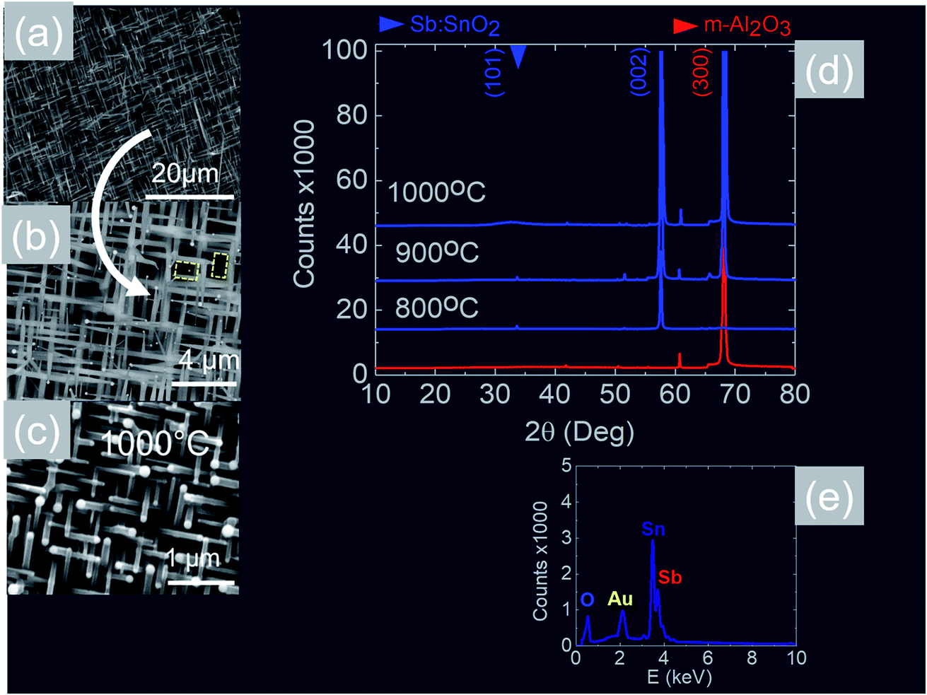 | ||
| Fig. 2 SEM images of the Sb:SnO2 NWs obtained at (a), (b) 800 °C and (c) 1000 °C on m-Al2O3 (d) XRD of m-Al2O3 (red) and Sb:SnO2 NWs (blue) grown on m-Al2O3 at 800 °C, 900 °C and 1000 °C (e) EDX of the Sb:SnO2 NWs. | ||
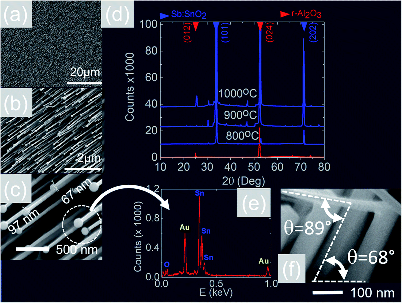 | ||
| Fig. 3 (a)–(c) SEM images of the Sb:SnO2 NWs obtained at 800 °C on r-Al2O3 (d) XRD of r-Al2O3 and Sb:SnO2 NWs grown at 800 °C , 900 °C and 1000 °C (e) EDX of an Au:Sn particle on the end of a Sb:SnO2 NW (f) side view showing that the first segment of the Sb:SnO2 NWs grows at θ = 68° and the second segment at θ = 89° with respect to the first. | ||
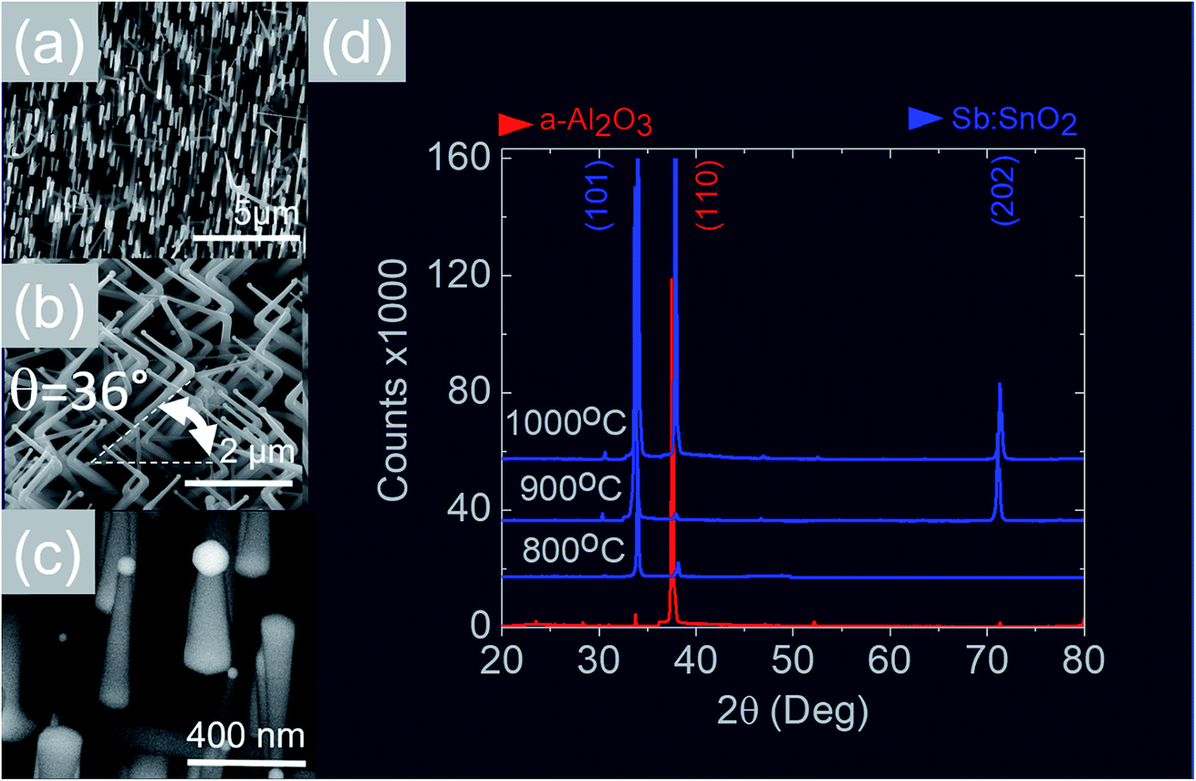 | ||
| Fig. 4 (a)–(c) SEM images of the Sb:SnO2 NWs obtained at 800 °C on a-Al2O3 (d) XRD of a-Al2O3 (red) and Sb:SnO2 NWs (blue) grown on a-Al2O3 at 800 °C, 900 °C and 1000 °C. | ||
In all cases, we obtained a uniform distribution and ordering of Sb:SnO2 NWs over the 10 mm × 10 m-, r- and a-Al2O3 in reproducible way, using Sn/Sb = 0.1 at 800 °C and 1 mbar as described above. Subsequently we varied the growth temperature between 700 °C to 1000 °C in order to find if any changes occur in the growth directions and ordering. The Sb:SnO2 NWs obtained at 900 °C on m-Al2O3 were very similar to those obtained at 800 °C, but we find that the Sb:SnO2 NWs obtained at 1000 °C are short, as shown in Fig. 2(c), due to the fact that the Sn and Sb are more or less completely transferred into the gas stream under the flow of Ar during the temperature ramp, before the onset of one dimensional growth. In fact, the depletion of Sb during the temperature ramp is more significant than Sn, due to the fact that Sn has a melting point of 232 °C and vapor pressure of 10−5 mbar, while Sb has a higher melting point of 630 °C, but a remarkably higher vapor pressure of 10−1 mbar at 1000 °C. This in turn implies an important doping limitation when trying to obtain high carrier densities and conductivity in Sb:SnO2 NWs using metallic Sn and Sb.34 Likewise, the Sb:SnO2 NWs obtained on m-Al2O3 at 700 °C were short, similar to those obtained at 1000 °C, due to the limited supply of Sn which has a lower vapor pressure at 700 °C, but they remained orthogonally oriented to each other. No changes occurred in the morphology and growth directions of the Sb:SnO2 NWs on r- and a-Al2O3 by varying the temperature between 700 °C and 1000 °C. In contrast, the epitaxial growth and ordering of the Sb:SnO2 NWs was critically dependent on the mass ratio of Sn/Sb. We obtained ordered Sb:SnO2 NWs on m-, r- and a-Al2O3 only for Sn/Sb = 0.15 ± 0.05. One dimensional growth was completely suppressed when Sn/Sb < 0.1, and the Sb:SnO2 NWs were not oriented in any particular direction for Sn/Sb > 0.2. Before elaborating further, it is important to mention that we did not obtain any Sb:SnO2 NWs at all without adding O2 to the flow of Ar during the growth step. In other words, the residual or background O2 after purging and the temperature ramp was not significant, and the growth of the Sb:SnO2 NWs occurred solely due to the oxygen supplied during the growth step.
Consequently the suppression of one dimensional growth for Sn/Sb < 0.1 is attributed to the total depletion and transfer of Sn into the gas stream during the temperature ramp, before the onset of growth, as it forms a liquid alloy with Sb. Note also that we did not obtain any SbO2, Sb2O3 or Sb2O5 NWs by using only Sb.
On the other hand the Sb:SnO2 NWs were not oriented in any particular direction for Sn/Sb > 0.2. From the above it is clear that an excess of Sb mixed with Sn provides flexible control over the Sn supplied to the Au particles which must be carefully tuned to a minimum for epitaxial growth and ordering to occur. This is further corroborated by the fact that we did not obtain ordered Sb:SnO2 NWs without mixing the Sb and Sn even when Sn/Sb ≈ 0.15 ± 0.05.
In addition to the above it is important to point out that the epitaxial growth and ordering of the Sb:SnO2 NWs also depends critically on the crystal quality of the m, r and a-Al2O3 surfaces. It has been shown that m-Al2O3 is thermodynamically unstable during high-temperature growth and nanostructured grooves composed of s- and r-facets develop along the [11![[2 with combining macron]](https://www.rsc.org/images/entities/char_0032_0304.gif) 0] direction.35 In contrast Wang et al.31 claimed that both the a- and r-plane of Al2O3 retain their surface structure at elevated temperatures. We annealed the m-, r- and a-Al2O3 at 1000 °C for 30 min under Ar and O2 without any Sn, Sb or Au and observed a drastic reduction in the strength of the XRD peaks of the m- and a-Al2O3 but the r-Al2O3 appeared to maintain its surface crystallinity. Subsequently we deposited 1 nm of Au over the pre-annealed m-, r- and a-Al2O3 and tried to grow epitaxial, ordered Sb:SnO2 NWs at 800 °C and 1 mbar using Sn/Sb = 0.1. As expected, we obtained ordered Sb:SnO2 only on r-Al2O3. It appears then, that the deposition of 1 nm Au over pristine m-, r-, and a-Al2O3 at room temperature, prevents in some way the deterioration of the surface crystal structure and allows the epitaxial growth of ordered Sb:SnO2 NWs at elevated temperatures between 700 °C to 1000 °C. In fact, the deposition of a 1 nm Au layer on the m-, r-, and a-Al2O3, which contain grooves or steps along specific crystallographic directions, leads to instabilities and ruptures of the Au at elevated temperatures as described by Hughes et al.36 These ruptures occur at high curvature sites, i.e., peaks and ridges, which act as retracting edges leading to a net flux of atoms away from the high positive curvature regions. For sufficiently thin layers, this process exposes the texture or steps of the underlying substrate, and a self-assembly of the Au particles will occur along specific crystallographic orientations.37 This in turn will instigate one dimensional epitaxial growth along specific lateral crystallographic directions via the VLS mechanism, as shown in Fig. 1(b). When Sn is added to the Au particles, it is expected to reduce the surface tension and contact angle θ with the underlying m-, r- and a-Al2O3 surface, as a consequence of the fact that Sn and Sb have surface tensions of ≈500 mN m−1 and 350 mN m−1 respectively, but the surface tension of Au is ≈1000 mN m−1. A large contact angle implies that the contact area is small, and vice versa, a smaller contact angle implies a larger contact area. Consequently, an excess of Sn is expected to lead to the formation of Au–Sn particles having a small contact angle and larger contact area with the underlying m, r and a-Al2O3 surface, in which case they might not be able to follow the variations in the surface topography which is necessary to obtain ordered Sb:SnO2 NWs. The formation of ordered Sb:SnO2 NWs is possible due to a reduction of the Sn by the excess of Sb during the temperature ramp, which in turn results into sufficiently small Au–Sn liquid particles that are able to follow steps or grooves on the surface during the growth step at elevated temperatures. Epitaxial growth, then, commences laterally, after which a transition to inclined growth occurs leading to the formation of the ordered networks of Sb:SnO2 NWs shown in Fig. 2, 3 and 4.
0] direction.35 In contrast Wang et al.31 claimed that both the a- and r-plane of Al2O3 retain their surface structure at elevated temperatures. We annealed the m-, r- and a-Al2O3 at 1000 °C for 30 min under Ar and O2 without any Sn, Sb or Au and observed a drastic reduction in the strength of the XRD peaks of the m- and a-Al2O3 but the r-Al2O3 appeared to maintain its surface crystallinity. Subsequently we deposited 1 nm of Au over the pre-annealed m-, r- and a-Al2O3 and tried to grow epitaxial, ordered Sb:SnO2 NWs at 800 °C and 1 mbar using Sn/Sb = 0.1. As expected, we obtained ordered Sb:SnO2 only on r-Al2O3. It appears then, that the deposition of 1 nm Au over pristine m-, r-, and a-Al2O3 at room temperature, prevents in some way the deterioration of the surface crystal structure and allows the epitaxial growth of ordered Sb:SnO2 NWs at elevated temperatures between 700 °C to 1000 °C. In fact, the deposition of a 1 nm Au layer on the m-, r-, and a-Al2O3, which contain grooves or steps along specific crystallographic directions, leads to instabilities and ruptures of the Au at elevated temperatures as described by Hughes et al.36 These ruptures occur at high curvature sites, i.e., peaks and ridges, which act as retracting edges leading to a net flux of atoms away from the high positive curvature regions. For sufficiently thin layers, this process exposes the texture or steps of the underlying substrate, and a self-assembly of the Au particles will occur along specific crystallographic orientations.37 This in turn will instigate one dimensional epitaxial growth along specific lateral crystallographic directions via the VLS mechanism, as shown in Fig. 1(b). When Sn is added to the Au particles, it is expected to reduce the surface tension and contact angle θ with the underlying m-, r- and a-Al2O3 surface, as a consequence of the fact that Sn and Sb have surface tensions of ≈500 mN m−1 and 350 mN m−1 respectively, but the surface tension of Au is ≈1000 mN m−1. A large contact angle implies that the contact area is small, and vice versa, a smaller contact angle implies a larger contact area. Consequently, an excess of Sn is expected to lead to the formation of Au–Sn particles having a small contact angle and larger contact area with the underlying m, r and a-Al2O3 surface, in which case they might not be able to follow the variations in the surface topography which is necessary to obtain ordered Sb:SnO2 NWs. The formation of ordered Sb:SnO2 NWs is possible due to a reduction of the Sn by the excess of Sb during the temperature ramp, which in turn results into sufficiently small Au–Sn liquid particles that are able to follow steps or grooves on the surface during the growth step at elevated temperatures. Epitaxial growth, then, commences laterally, after which a transition to inclined growth occurs leading to the formation of the ordered networks of Sb:SnO2 NWs shown in Fig. 2, 3 and 4.
All of the Sb:SnO2 NWs on m-, r- and a-Al2O3 exhibited clear and well resolved peaks in the XRD, as shown in Fig. 2(d), 3(d) and 4(d) respectively, corresponding to the tetragonal rutile crystal structure of SnO2. For comparison, we have included the XRD of the m-, r- and a-Al2O3 without the Sb:SnO2 NWs. More specifically, the Sb:SnO2 NWs on m-, r- and a-Al2O3 exhibit only one or two major peaks in their XRD, consistent with the fact that they grow along specific crystallographic directions. In contrast, we observed a multitude of major peaks from the Sb:SnO2 NWs on c-Al2O3, due to the fact that they do not grow in an epitaxial fashion along specific directions, see ESI.† We did not observe any peaks related to oxides of Sb such as Sb2O3 or Sb2O5 which have melting points of 656 °C and 380 °C respectively. In addition, we do not observe any peaks suggesting the formation of Sb2O4, i.e. SbO2 which is known to break down into Sb and O2 at a higher temperature of 930 °C. Nevertheless the Sb:SnO2 NWs contain Sb donor impurities as shown by the EDX spectrum in Fig. 2(e) and as confirmed previously by Raman spectroscopy.34 Small differences in the amount of metallic Sb, i.e. for Sn/Sb = 0.15 ± 0.05, did not change the crystal structure or orientation of the Sb:SnO2 NWs. We obtained exactly the same XRD spectra shown in Fig. 2, 3 and 4 for Sn/Sb = 0.1 and Sn/Sb = 0.15. However, it is important to point out that we did not detect any Sb in the Au particles on the ends of the Sb:SnO2 NWs, as shown by the EDX spectrum in Fig. 3(e). This is consistent with the fact that we did not find Sb in the Au after trying to grow Sb2O3, Sb2O5 or SbO2 NWs, using just Sb, and leads us to suggest that the Sb donor impurities are incorporated into the SnO2 NWs by surface diffusion, from their sides, as depicted in Fig. 1(c).
Now, the Sb:SnO2 NWs on m-Al2O3 exhibited one dominant peak in the XRD, as shown in Fig. 2(d), corresponding to the (002), i.e. a multiple of (001), crystallographic planes of tetragonal rutile SnO2. The two dimensional lattice of (001) SnO2 and the oxygen terminated surface of m-Al2O3 are shown in Fig. 5(a) and (b) respectively. These have a small lattice mismatch of 0.5% so the Sb:SnO2 NWs grow by a stacking of (001) planes on m-Al2O3 and the in-plane epitaxial relationship is SnO2 (001)‖m-Al2O3. The growth of the Sb:SnO2 NWs on m-Al2O3 is identical to that of SnO2 NWs obtained by Leonardy et al.27 on m-Al2O3 using SnO as opposed to Sn. For completeness, the tetragonal unit cell of SnO2 is shown in Fig. 5(c), from which one may observe that the (101) crystallographic plane of SnO2 is inclined at θ = 34° with respect to the (001). The Sb:SnO2 NWs have rectangular sections, as shown in Fig. 5(d), and grow along the [101] crystallographic direction as confirmed by the HRTEM image of Fig. 5(e). Hence the Sb:SnO2 NWs are inclined at θ = 34° with respect to the surface of m-Al2O3, and the fourth fold symmetry of the m-Al2O3 surface lattice gives rise to Sb:SnO2 NWs oriented along two mutually orthogonal directions and the formation of the mesh structure observed in Fig. 2(a)–(c). This has also been confirmed by Wang et al.31 who showed that un-doped SnO2 NWs also grow laterally along two perpendicular directions and cross each other on m-Al2O3.
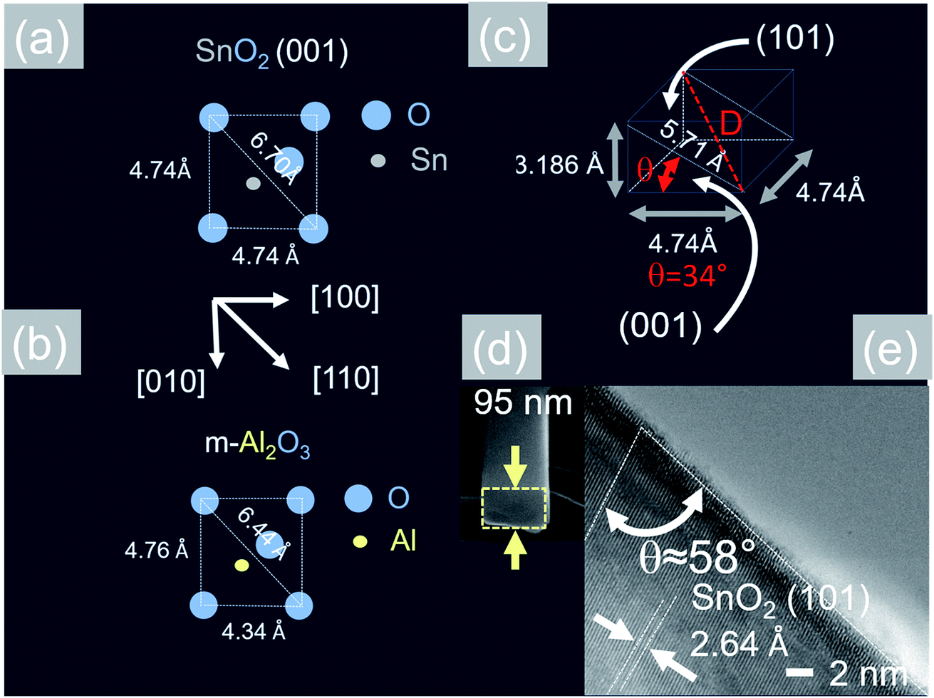 | ||
| Fig. 5 (a) Two dimensional lattice of the SnO2 (001) that is grown in an epitaxial way on (b) oxygen terminated m-Al2O3 (c) crystal structure of tetragonal rutile SnO2 (d) TEM and (e) HRTEM images of a Sb:SnO2 NW after removing it from the m-Al2O3. | ||
In contrast to the above we find that the Sb:SnO2 NWs on r-Al2O3 exhibited two dominant peaks in the XRD, as shown in Fig. 3(d), corresponding to the (101) and (202) crystallographic planes of tetragonal rutile SnO2. The two dimensional lattice of (101) SnO2 and the oxygen terminated surface of r-Al2O3 are shown in Fig. 6(a) and (b) respectively. These have a larger lattice mismatch of 11%, and the in-plane epitaxial relationship is SnO2 (101)‖r-Al2O3. The growth of the Sb:SnO2 NWs on r-Al2O3 is very similar to the un-doped SnO2 NWs of Kim et al.38 which were also inclined at θ = 68° on r-Al2O3. Lateral SnO2 NWs have also been obtained via the VLS mechanism by Kim et al.29 on r-Al2O3 using C and SnO2 as opposed to Sn but they did not observe the transition of growth from lateral to vertical SnO2 NWs.
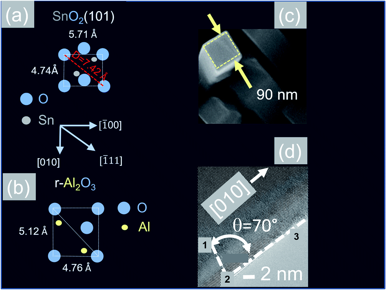 | ||
| Fig. 6 (a) Two dimensional surface lattice of SnO2 (101) which grows on (b) oxygen terminated surface of r-Al2O3 (c) TEM image of Sb:SnO2 NWs after removing from r-Al2O3 (d) HRTEM image of the Sb:SnO2 NWs showing the (010) lattice planes. | ||
3.2 Selective area location growth of Sb:SnO2 NWs on r-Al2O3
The VLS growth mechanism permits selective area location growth on m-, r- and a-Al2O3 as we did not obtain any Sb:SnO2 NWs without using Au. We obtained hexagonally ordered Sb:SnO2 NWs on r-Al2O3 by drop casting ∼10 μl of 9 μm diameter polystyrene spheres on r-Al2O3, followed by the deposition of a thin layer of ∼1 nm Au as shown in Fig. 7. Subsequently, the spheres were removed in isopropanol by ultrasonic vibration for 1 min, and the Sb:SnO2 NWs were grown on the patterned Au on r-Al2O3 at 800 °C. The Sb:SnO2 NWs on r-Al2O3 do not consist of two segments due to the reduced growth time. One may clearly observe that the Sb:SnO2 NWs grow on the r-Al2O3 in a hexagonal pattern suggesting that one may also obtain different geometries in order to tailor the absorption–transmission spectrum in novel devices such as NWSCs.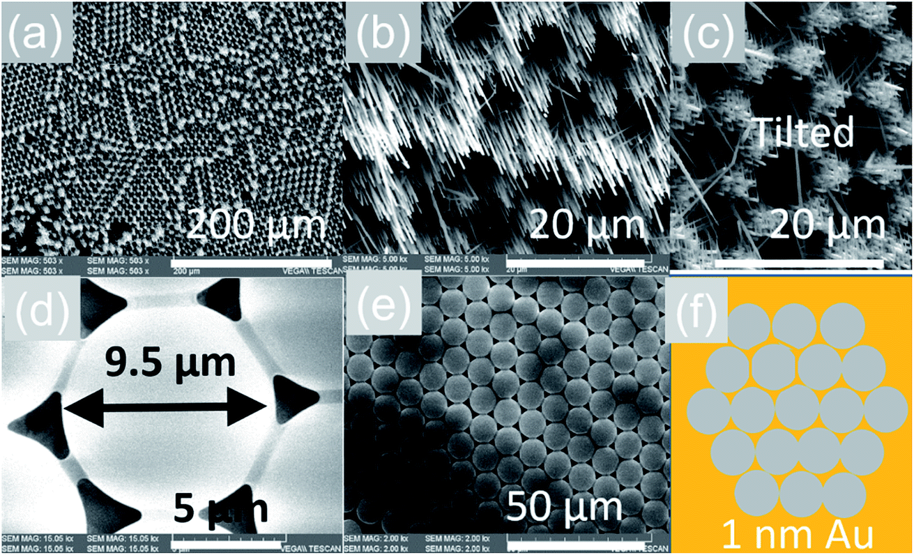 | ||
| Fig. 7 Selective area location growth of Sb:SnO2 NWs on r-Al2O3 (a) low magnification and (b) high magnification image (c) tilted view of the Sb:SnO2 NWs on r-Al2O3 showing that they do not consist two segments as shown in Fig. 3(f); (d) an individual sphere in contact with its six closest neighbors (e) domain of ordered spheres (f) schematic representation of the spheres on r-Al2O3 after the deposition of 1 nm Au in between the spheres. | ||
3.3 Electrical properties of Sb:SnO2 NWs on m-, r- and a-Al2O3
The carrier density of the Sb:SnO2 NWs grown on m-, r- and a-Al2O3 at 800 °C and 1 mbar with Sn/Sb = 0.1 was measured by the Hall effect. We obtained a carrier density of 8 × 1019 cm−3 which is significantly larger than that measured previously in un-doped SnO2 NWs, that was of the order of 1016 cm−3.33 The conductivity of the Sb:SnO2 NWs was found to be ≈3 × 10² (Ω cm)−1 giving a mobility of 20 cm2 V−1 s−1 which is lower compared to 70 cm2 V−1 s−1 in un-doped SnO2 NWs that was previously measured by THz conductivity spectroscopy.33 We did not observe a significant variation in the carrier density of the Sb:SnO2 NWs on m-, r- and a-Al2O3, or due to slight variations of Sn/Sb = 0.15 ± 0.05. We measured the Hall effect of the Sb:SnO2 NWs obtained with Sn/Sb = 0.15 and found a carrier density of 8.3 × 1019 cm−3 which is very close to that obtained with Sn/Sb = 0.1. However the carrier density in the Sb:SnO2 NWs obtained at 900 °C was smaller i.e. 6 × 1018 cm−3 while those obtained at 1000 °C had an even smaller carrier density of 4 × 1017 cm−3 and conductivity of ≈3 (Ω cm)−1. This is attributed to the transfer of the Sb into the gas stream during the temperature ramp, and before the onset of one dimensional growth, due to the high vapor pressure of Sb, which in turn limits the supply and incorporation of Sb impurities into the SnO2 NWs during the growth step. This trend is consistent with the findings of Klamchuen et al.,22 who found that the doping level in SnO2 NWs grown at 650 °C was twice that obtained at 750 °C, attributed to a suppression of impurity re-evaporation. They also observed that the doping level did not increase further upon reducing the growth temperature from 650 °C to 550 °C, which was explained by a suppression of the diffusion length of impurity ad-atoms on the surface of the SnO2 NWs, and the presence of a temperature activated energy barrier which is necessary for the incorporation of the Sb impurities into the host lattice of SnO2.We suggest that the incorporation of Sb impurities into the SnO2 NWs occurs through the sides of the SnO2 NWs by thermal diffusion, or, via the triple phase junction, as shown in Fig. 1(c), similar to the mechanism proposed by Klamchuen et al.22 This is also corroborated by the fact that we did not detect any Sb in the Au particles after attempting to grow SbO2, Sb2O3 or Sb2O5 NWs on r-Al2O3, by using only Sb, and also by the fact that we did not detect any Sb in the Au:Sn particles on the ends of the Sb:SnO2 NWs, as shown in Fig. 3(e). It is also consistent with the findings of McGinley et al.,39 who showed that the surface of SnO2 nanoparticles is terminated by an oxygen rich layer, but when doped n-type with 9% or 17% Sb, the impurity atoms are concentrated near the surface of the SnO2 nanoparticles with an oxidation state of five.
In order to obtain a more detailed understanding of the electronic properties of the Sb:SnO2 NWs we carried out electronic structure calculations from first principles using the CASTEP plain wave DFT code40,41 and the Heyd–Scuseria–Ernzerhof (HSE)42 exchange correlate-correlation energy functional. After relaxation of the cell, we obtained lattice constants of a = b = 4.82 Å and c = 3.23 Å which are in close agreement to reported values.42 DOS calculations were performed for the case of (a) the perfect SnO2 cell and (b) the Sb-doped SnO2 cell, shown in Fig. 8(a) and (b) respectively. The maximum of the valence band (VB) is set at zero energy level. It is evident from the partial density of states shown in Fig. 8(a) and (b) that the VB is dominated by O and the CB by Sn.60 The band gap was found to be 3.6 eV for the perfect structure but a slight reduction of the band gap down to 3.5 eV was observed with doping. This semi-empirical method yields a much more accurate band gap than calculations performed based on the Perdew–Burke–Ernzerhof (PBE) GGA functional which are not shown here. In addition we find that the incorporation of Sb into the SnO2 crystal does not produce any deep levels within the band gap which are in general detrimental to the operation of optoelectronic devices such as solar cells, light emitting diodes etc. In other words the Sb impurities are incorporated into the SnO2 lattice as substitutional donors and our calculations show that the Fermi level resides 0.46 eV above the CB edge for 12.5 at% Sb (≡4 × 1021 cm−3).
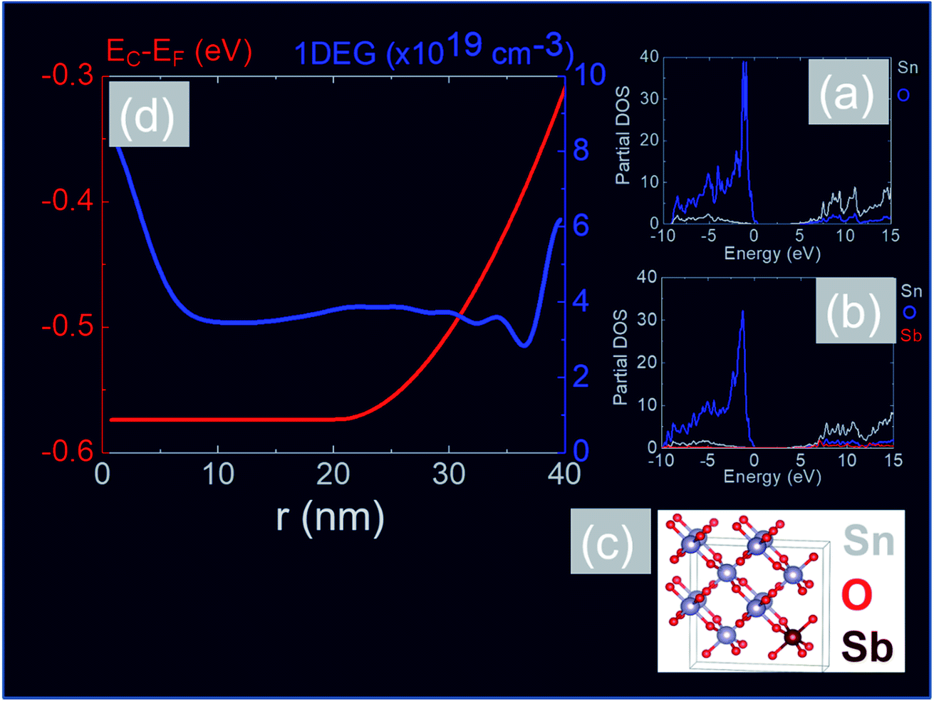 | ||
| Fig. 8 (a) DOS for un-doped SnO2 and (b) DOS for Sb:SnO2 with 12.5 at% (≡4 × 1021 cm−3) (c) structural model showing Sb substitutional donor impurity in SnO2 (d) SCPS CB potential profile (red) and 1DEG charge distribution (blue) versus distance along the radial direction of a Sb:SnO2 NWs with a diameter of 80 nm taking EC − EF = −0.3 eV at the surface and assuming a uniform distribution of ionized donor impurities ND+ = 1 × 1019 cm−3 between r = 20 and 40 nm. | ||
In addition, we calculated the conduction band (CB) potential profile, and one dimensional electron gas (1DEG) charge distribution, along the radial direction, via the self-consistent solution of the Poisson–Schrödinger (SCPS) equations, in the effective mass approximation, as described in detail elsewhere.43 The SCPS calculations were carried out by taking into account the effective mass and dielectric constant of SnO2 , i.e. (ref. 44 and 45) and εr = 13.5 (ref. 46 and 47) respectively. In order to obtain a carrier density of 8 × 1019 cm−3 as determined from the Hall effect we have taken the Fermi level to be energetically located ≈0.3 eV above the CB edge, at the surface of the Sb:SnO2 NWs. This is consistent with the electronic structure calculations of Mishra et al.,48 who showed that the Sb impurities in SnO2 form a band, which has an energetic overlap with the conduction band and a nearly free electron structure, i.e. behaves like a metallic band. It is also consistent with Li et al.,49 who calculated the electronic structure of Sb:SnO2 for 6.25% Sb, and found that the Fermi level moves into the CB upon the incorporation of Sb, and displays metallic character, but also with Farahani et al.,50 who showed that the Fermi level resides ≈0.33 eV above the CB edge at the surface of Sb:SnO2 epitaxial layers grown by molecular beam epitaxy on r-Al2O3.
The CB potential profile with respect to the Fermi level, i.e. EC − EF and 1DEG charge distribution, versus distance along the radial direction of the Sb:SnO2 NWs, is shown in Fig. 8(d), where we have taken the donor impurities to be confined between r = 20 and 40 nm. The CB edge potential profile is near flat band in the vicinity of the core and the 1DEG charge distribution has a maximum at the core and a local maximum at the surface. It should be noted that we obtain similar band profiles and charge distributions by taking a uniform distribution of Sb impurities throughout the Sb:SnO2 NWs. However the 1DEG in the vicinity of the core is expected to have a higher mobility when the density of donor impurities is larger at the surface than the core, as is the case in Fig. 9(d). In other words, the incorporation of Sb impurities into the SnO2 NWs via surface diffusion is not a drawback in the end. We estimate that the mobility in the Sb:SnO2 NWs with a maximum carrier density of the order of 1020 cm−3 is a few tens of cm2 V−1 s−1 (ref. 23 and 24) so the resistivity of the Sb:SnO2 NWs is of the order of 10−3 Ω cm which in turn is attractive for the deposition of metal contacts with low resistance and the fabrication of high performance devices.
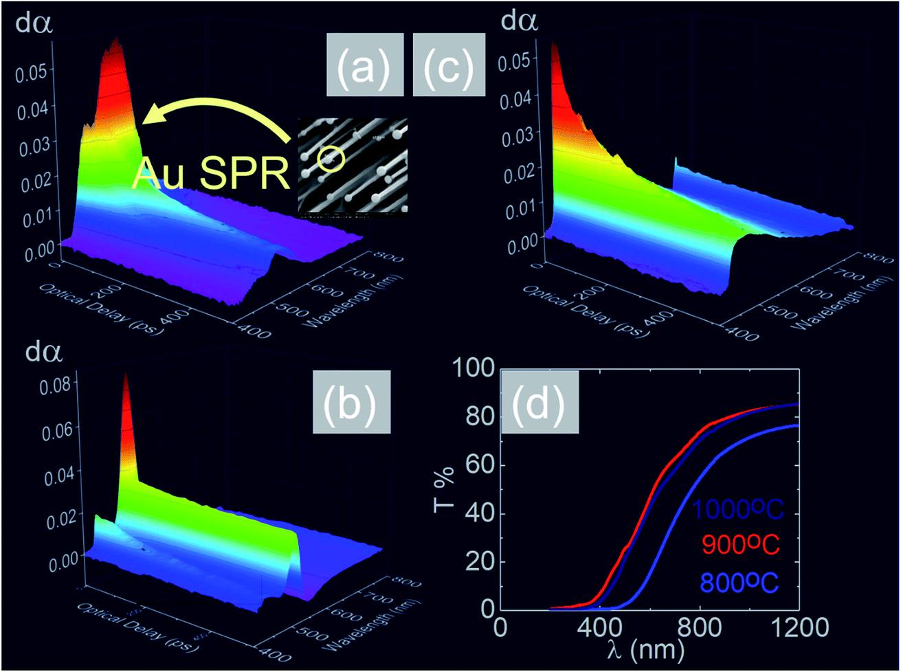 | ||
| Fig. 9 Ultrafast, differential transient absorption dα versus optical delay τ (ps) and probe wavelength λ (nm) through the Sb:SnO2 NWs grown on r-Al2O3 at (a) 800 °C, (b) 900 °C and (c) 1000 °C; (d) steady state transmission of light through the Sb:SnO2 NWs grown on r-Al2O3 at different temperatures. | ||
3.4 Optical properties of Sb:SnO2 NWs on m-, r- and a-Al2O3
In the past the transmission of light through Sb:SnO2 NWs14–24 has not been investigated as they were not ordered or oriented along any particular direction which in turn leads to a considerable suppression of transmission and transparency. In contrast a higher transmission of light is expected to occur through ordered MO NWs. We measured the steady state transmission through the Sb:SnO2 NWs that were grown at 800 °C on r-Al2O3 as shown in Fig. 9(d). The Sb:SnO2 NWs have an optical transmission of 80% above 800 nm but they absorb light in the visible between 400 nm to 800 nm. We do not observe any interference effects since the spacing between the Sb:SnO2 NWs is considerably smaller than the wavelength of light. In addition we find that the Sb:SnO2 NWs on r-Al2O3 obtained at 900 °C and 1000 °C have a higher transparency compared to those obtained at 800 °C due to their shorter lengths. In order to understand the origin of the absorption we have measured the transient absorption through the Sb:SnO2 NWs on an fs time scale as shown in Fig. 9(a)–(c). In all cases, we observe a strong peak in the time evolution of the differential absorption between 500 nm and 600 nm attributed to the surface plasmon resonance (SPR) of the Au–Sn particles, corresponding to sizes between 10 nm and 100 nm (ref. 51) and the existence of surface states lying energetically in the energy gap of SnO2.52 One may observe a slight blue shift of the peak from 900 °C to 1000 °C in Fig. 9(b) and (c), consistent with that observed in the steady state transmission, that might be related to the smaller size of the Au–Sn particles due to the depletion of Sn that occurs during the temperature ramp and/or the elimination of mid gap states at elevated temperatures. It is important to point out, that the transparency of the Sb:SnO2 NWs on r-Al2O3 may be increased further by selective area location growth as shown in Fig. 7 which leads to a higher transmission through the voids between the Sb:SnO2 NW.Finally it is worthwhile considering the PL obtained from the Sb:SnO2 NWs, grown on r-Al2O3 at 800 °C, as shown in Fig. 10(a), in which case we observe emission at λ = 600 nm (≡2.1 eV) and 300 K. Bulk SnO2 has a direct energy band gap of 3.7 eV but the even – parity symmetry of the conduction-band minimum and valence-band maximum states prohibits band – edge radiative transitions which has limited the use of SnO2 for the fabrication of light emitting diodes. The PL at 2.1 eV is attributed to radiative recombination between deep donor and acceptor like states residing energetically in the energy band gap of SnO2 that are related to oxygen vacancies. We observe a suppression of the maximum at λ = 600 nm and the emergence of emission at λ = 470 nm (≡2.6 eV) by decreasing the temperature from 300 K to 10 K due to radiative recombination via shallower levels as proposed by Luo et al.53 However an interesting aspect of the PL emission at 2.1 eV and 2.6 eV is that it has a lifetime of τ ≈ 0.2 ms as shown by the time resolved PL in Fig. 10(b). This is considerably higher than the lifetimes extracted from SnO2 rods and particles which are of the order of 100 ns (ref. 54) and comparable to Eu doped SnO2 nanocrystals.55 Hence, in principle, the Sb:SnO2 NWs described here may be processed into devices capable of light emission but also NWSCs.56,57
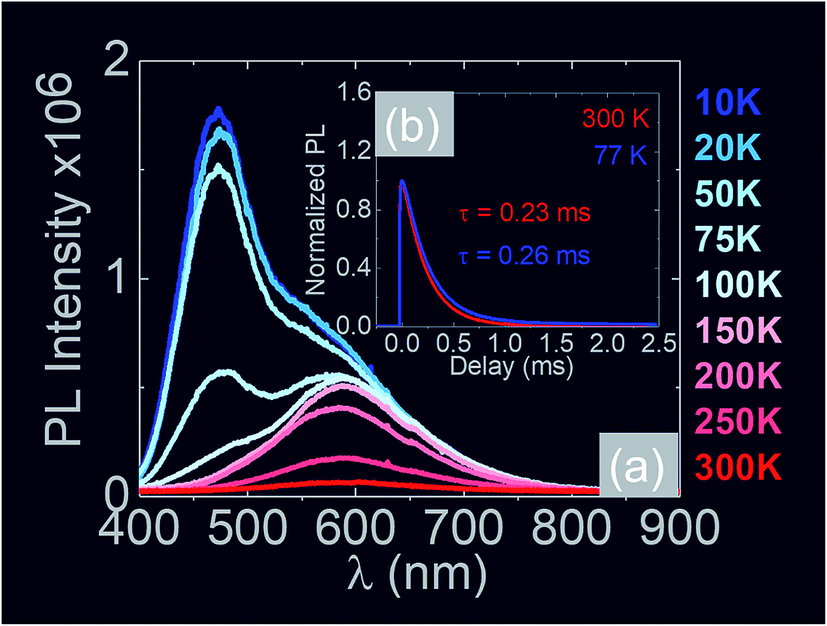 | ||
| Fig. 10 (a) Temperature dependence of the PL obtained from the Sb:SnO2 NWs grown on r-Al2O3 at 800 °C (b) time resolved PL taken at λ = 600 nm for 300 K and 77 K along with the corresponding lifetimes. | ||
To the best of our knowledge no one has previously used ordered networks of Sn:In2O3 or Sb:SnO2 NWs to make NWSCs despite the fact that Battaglia et al.58 has showed that periodic photonic nanostructures outperform their random counterparts in trapping light in solar cells. It is desirable then to use these highly conductive, ordered networks, of Sb:SnO2 NWs in order to improve the performance of all-solid state NWSCs. In addition the Sb:SnO2 NWs can be used in perovskite solar cells as an electron transport layer (ETL). According to Jiang et al.59 a traditional ETL such as TiO2, is not very efficient for charge extraction at the interface, especially in planar structures. In addition, the devices using TiO2 suffer from serious degradation under ultraviolet illumination. SnO2 shows a better band alignment with the perovskite absorption layer and higher electron mobility, which is helpful for electron extraction. Consequently the specific ordered networks of Sb:SnO2 NWs described here may serve as a scaffold on top of which one may deposit a perovskite absorber layer and a hole transport layer in order to create a p–n junction solar cell.
4 Conclusions
We have grown epitaxial, ordered Sb:SnO2 NWs via the VLS mechanism on m-, r- and a-Al2O3 between 700 °C and 1000 °C using metallic Sn containing an excess of Sb i.e. for Sn/Sb = 0.15 ± 0.05 under a flow of Ar and O2 at 1.5 ± 0.5 mbar. One dimensional growth was suppressed for Sn/Sb < 0.1 while the Sb:SnO2 NWs were not oriented along any particular direction for Sn/Sb > 0.2. Consequently highly conductive and directional Sb:SnO2 NWs may only be obtained in a narrow window of growth conditions. All of the Sb:SnO2 NWs have the tetragonal rutile crystal structure and square sections. The Sb:SnO2 NWs are oriented along two mutually perpendicular directions forming a rectangular mesh on m-Al2O3 with a maximum lattice mismatch of 0.1%. In contrast the Sb:SnO2 NWs on r-Al2O3 are all oriented in one direction but have a larger lattice mismatch of 10%. The morphology and growth directions of the Sb:SnO2 NWs on m-, r- and a-Al2O3 did not change by varying the growth temperature between 700 °C and 1000 °C but the carrier density changed from 8 × 1019 cm−3 to 4 × 1017 cm−3 due to the re-evaporation and limited incorporation of Sb donor impurities into the SnO2 NWs with increasing temperature. All of the Sb:SnO2 NWs had a high transmission of 80% above 800 nm and absorbed light between 400 nm to 800 nm primarily due to the SPR of the Au particles. The transmission may be improved significantly by selective area location growth which we have shown that is possible on r-Al2O3 by patterning the catalyst. In addition the Sb:SnO2 NWs on m-, r- and a-Al2O3 are capable of light emission with remarkably long lifetimes of 0.2 ms and are attractive for the realization of NWSCs.Conflicts of interest
There are no conflicts of interest to declare.References
- Q. Wan, E. N. Dattoli and W. Lu, Appl. Phys. Lett., 2007, 90, 222107 CrossRef.
- M. Zervos, C. Mihailescu, J. Giapintzakis, C. Luculescu, N. Florini, P. Komninou, J. Kioseoglou and A. Othonos, APL Mater., 2014, 2, 056104 CrossRef.
- S. N. Bai, H. H. Tsai and T. Y. Tseng, Thin Solid Films, 2007, 516, 155 CrossRef CAS.
- H. Duan, H. He, L. Sun, S. Song and Z. Ye, Nanoscale Res. Lett., 2013, 8(1), 493 CrossRef PubMed.
- C. O. Dwyer, M. Szachowicz, G. Visimberga, V. Lavayen, S. B. Newcomb and C. M. S. Torres, Nat. Nanotechnol., 2009, 4, 239 CrossRef PubMed.
- J. Gao, R. Chen, D. H. Li, L. Jiang, J. C. Ye, X. C. Ma, X. D. Chen, Q. H. Xiong, H. D. Sun and T. Wu, Nanotechnology, 2011, 22, 195706 CrossRef CAS PubMed.
- Q. Wan, E. N. Dattoli, W. Y. Fung, W. Guo, Y. Chen, X. Pan and W. Lu, Nano Lett., 2006, 6, 2909, DOI:10.1021/nl062213d.
- P. Nguyen, H. T. Ng, J. Kong, A. M. Cassell, R. Quinn, J. Li, J. Han, M. McNeil and M. Meyyappan, Nano Lett., 2003, 3, 925 CrossRef CAS.
- D. Tsokkou, A. Othonos and M. Zervos, Appl. Phys. Lett., 2012, 100, 133101 CrossRef.
- Q. Wan, E. Dattoli and W. Lu, Small, 2008, 4, 451 CrossRef CAS.
- Z. H. Luo, D. S. Tang, H. Kuo, Y. Fang, Y. Q. Chen, X. W. He, Y. H. Peng, H. J. Yuan and Y. Yang, Chin. Phys. B, 2010, 19, 026102 CrossRef.
- C. Amorim, C. Dalmaschio, E. Leite and A. Chiquito, J. Phys. D: Appl. Phys., 2014, 47, 045301 CrossRef.
- F. Ma, Y. Jiao, G. Gao, Y. Gu, A. Bilic, S. Sanvito and A. Du, ACS Appl. Mater. Interfaces, 2016, 8, 25667 CrossRef CAS PubMed.
- Q. Wan and T. H. Wang, Chem. Commun., 2005, 30, 3841 RSC.
- L. Li, J. Huang, T. Wang, H. Zhang, Y. Liu and J. Li, Biosens. Bioelectron., 2010, 25, 2436 CrossRef CAS.
- X. Rui-Jie and L. Hui-Xuan, Chin. Phys. B, 2012, 21, 088104 CrossRef.
- Q. Wan, J. Huang, Z. Xie, T. Wang, E. N. Dattoli and W. Lu, Appl. Phys. Lett., 2008, 92, 102101 CrossRef.
- J. Huang, A. Lu, B. Zhao and Q. Wan, Appl. Phys. Lett., 2007, 91, 073102 CrossRef.
- B. R. Sathe, M. Patil, P. S. Walke, J. P. Vivek, A. Lele, V. K. Pillai and I. S. Mulla, Sci. Adv. Mater., 2009, 1, 38 CrossRef CAS.
- S. T. Jean and Y. C. Her, J. Appl. Phys., 2009, 105, 024310 CrossRef.
- R. Kumar, K. Rao, K. Rajanna and A. Phani, Mater. Lett., 2013, 106, 164 CrossRef CAS.
- A. Klamchuen, T. Yanagida, K. Nagashima, S. Seki, K. Oka, M. Taniguchi and T. Kawai, Appl. Phys. Lett., 2009, 95, 053105 CrossRef.
- I. Costa, Y. Colmenares, P. Pizani, E. Leite and A. Chiquito, Chem. Phys. Lett., 2018, 695, 125 CrossRef CAS.
- I. Costa, E. Bernardo, B. Marangoni, E. Leite and A. Chiquito, J. Appl. Phys., 2016, 120, 225109 CrossRef.
- S. Mathur and S. Barth, Small, 2007, 3, 2070 CrossRef CAS PubMed.
- W. S. Kim, D. Kim, K. L. Choi, J. G. Park and S. H. Hong, Cryst. Growth Des., 2010, 10, 4747 Search PubMed.
- A. Leonardy, W. Z. Hung, D. S. Tsai, C. C. Chou and Y. S. Huang, Cryst. Growth Des., 2009, 9, 3958 CrossRef CAS.
- L. Mazeina, Y. N. Picard, J. D. Caldwell, E. R. Glaser and S. M. Prokes, J. Cryst. Growth, 2009, 311, 3158 CrossRef CAS.
- W. S. Kim, D. Kim and S. H. Hong, CrystEngComm, 2014, 16, 9340 RSC.
- Y. H. Choi, J. Na, J. S. Kim, M. K. Joo, G. T. Kim and P. S. Kang, J. Korean Phys. Soc., 2014, 65, 502 CrossRef CAS.
- X. Wang, N. Aroonyadet, Y. Zhang, M. Mecklenburg, X. Fang, H. Chen, E. Goo and C. Zhou, Nano Lett., 2014, 14, 3014 CrossRef CAS PubMed.
- E. P. Stuckert, R. H. Geiss, C. J. Miller and E. R. Fisher, ACS Appl. Mater. Interfaces, 2016, 8, 22345 CrossRef CAS PubMed.
- D. Tsokkou, A. Othonos and M. Zervos, Appl. Phys. Lett., 2012, 100, 133101 CrossRef.
- M. Zervos, A. Othonos, E. Tanasa and E. Vasile, J. Phys. Chem. C, 2018, 122, 22709 CrossRef CAS.
- D. Tsivion, M. Schvartzman, R. Popovitz-Biro and E. Joselevich, ACS Nano, 2012, 6, 6433 CrossRef CAS PubMed.
- R. A. Hughes, E. Menumerov and S. Neretina, Nanotechnology, 2017, 28, 282002 CrossRef PubMed.
- A. L. Giermann and C. V. Thompson, Appl. Phys. Lett., 2005, 86, 121903 CrossRef.
- W. S. Kim, D. H. Kim, Y. G. Jang and S. H. Hong, CrystEngComm, 2012, 14, 1545 RSC.
- C. McGinley, S. A. Moussalami, M. Riedler, M. Pflughoe, H. Borchert, M. Haase, A. R. B. Castro, H. Weller and T. Möller, Eur. Phys. J. D, 2001, 16, 225 CrossRef CAS.
- M. D. Segall, P. J. D Lindan, M. J. Probert, C. J. Pickard, P. J. Hasnip, S. J. Clark and M. C. Payne, J. Phys.: Condens. Matter, 2002, 14, 2717 CrossRef CAS.
- S. J. Clark, M. D. Segall, C. J. Pickard, P. J. Hasnip, M. J. Probert, K. Refson and M. C. Payne, Z. Kristallogr., 2005, 220, 567 CAS.
- W. Korner, D. F. Urban, D. M. Ramo, P. D. Bristowe and C. Elsasser, Phys. Rev. B: Condens. Matter Mater. Phys., 2014, 90, 195142 CrossRef.
- M. Zervos and L. F. Feiner, J. Appl. Phys., 2004, 95, 1 CrossRef.
- K. J. Button, C. G. Fonstad and W. Debrodt, Phys. Rev. B: Solid State, 1971, 4, 4539 CrossRef.
- Y. Mi, H. Odaka and S. Iwata, Jpn. J. Appl. Phys., Part 1, 1999, 38, 3453 CrossRef CAS.
- H. J. Daal, J. Appl. Phys., 1968, 39, 4467 CrossRef.
- M. Batzill and U. Diebold, Prog. Surf. Sci., 2005, 79, 47 CrossRef CAS.
- K. C. Mishra, K. H. Johnson and P. C. Schmidt, Phys. Rev. B: Condens. Matter Mater. Phys., 1995, 51, 13972 CrossRef CAS.
- Z. Q. Li, Y. L. Yin, X. D. Liu, L. Y. Li, H. Liu and Q. G. Song, J. Appl. Phys., 2009, 106, 083701 CrossRef.
- S. Farahani, T. Veal, J. Mudd, D. Scanlon, G. Watson, O. Bierwagen, M. White, J. Speck and C. McConville, Phys. Rev. B: Condens. Matter Mater. Phys., 2014, 90, 155413 CrossRef.
- S. Link and M. El-Sayed, J. Phys. Chem. B, 1999, 103, 4212 CrossRef CAS.
- A. Othonos, M. Zervos and D. Tsokkou, Nanoscale Res. Lett., 2009, 4, 828 CrossRef CAS PubMed.
- S. Luo, P. K. Chu, W. Liu, M. Zhang and C. Lin, Appl. Phys. Lett., 2006, 88, 183112 CrossRef.
- A. Kar, S. Kundu and A. Patra, J. Phys. Chem. C, 2011, 115, 118 CrossRef CAS.
- A. Kar and A. Patra, J. Phys. Chem. C, 2009, 113, 4375 CrossRef CAS.
- M. Zervos, E. Vasile, E. Vasile, E. Karageorgou and A. Othonos, J. Phys. Chem. C, 2016, 120, 11 CrossRef CAS.
- E. Karageorgou, M. Zervos and A. Othonos, APL Mater., 2014, 2, 116107 CrossRef.
- C. Battaglia, C. M. Hsu, K. Soderstrom, J. Escarre, F. J. Haug, M. Charriere, M. Boccard, M. Despeisse, D. T. L. Alexander, M. Cantoni, Y. Cui and C. Ballif, ACS Nano, 2012, 6, 2790 CrossRef CAS PubMed.
- Q. Jiang, X. Zhang and J. You, Small, 2018, 14, 1801154 CrossRef PubMed.
- J. Robertson, J. Phys. C: Solid State Phys., 1979, 12, 4767 CrossRef CAS.
Footnote |
| † Electronic supplementary information (ESI) available. See DOI: 10.1039/c9na00074g |
| This journal is © The Royal Society of Chemistry 2019 |