 Open Access Article
Creative Commons Attribution 3.0 Unported Licence
Multi-functional MnO2 nanomaterials for photo-activated applications by a plasma-assisted fabrication route†
Davide
Barreca
 *a,
Filippo
Gri
 b,
Alberto
Gasparotto
 b,
Giorgio
Carraro
 b,
Lorenzo
Bigiani
 b,
Thomas
Altantzis
 c,
Boštjan
Žener
 d,
Urška
Lavrenčič Štangar
 de,
Bruno
Alessi
 f,
Dilli Babu
Padmanaban
f,
Davide
Mariotti
f,
Dilli Babu
Padmanaban
f,
Davide
Mariotti
 f and
Chiara
Maccato
 *b
*b
aCNR-ICMATE and INSTM, Department of Chemical Sciences, Padova University, Via Marzolo 1, 35131 Padova, Italy. E-mail: davide.barreca@unipd.it
bDepartment of Chemical Sciences, Padova University and INSTM, Via Marzolo 1, 35131 Padova, Italy. E-mail: chiara.maccato@unipd.it
cEMAT, University of Antwerp, 2020 Antwerpen, Belgium
dFaculty of Chemistry and Chemical Technology, University of Ljubljana, 1000 Ljubljana, Slovenia
eLaboratory for Environmental and Life Sciences, University of Nova Gorica, 5000 Nova Gorica, Slovenia
fNanotechnology & Integrated Bio-Engineering Centre (NIBEC), Ulster University, BT37 0QB, UK
First published on 10th October 2018
Abstract
Supported MnO2-based nanomaterials were fabricated on fluorine-doped tin oxide substrates using plasma enhanced-chemical vapor deposition (PE-CVD) between 100 °C and 400 °C, starting from a fluorinated Mn(II) diamine diketonate precursor. Growth experiments yielded β-MnO2 with a hierarchical morphology tuneable from dendritic structures to quasi-1D nanosystems as a function of growth temperature, whose variation also enabled a concomitant tailoring of the system fluorine content, and of the optical absorption and band gap. Preliminary photocatalytic tests were aimed at the investigation of photoinduced hydrophilic (PH) and solid phase photocatalytic (PC) performances of the present nanomaterials, as well as at the photodegradation of Plasmocorinth B azo-dye aqueous solutions. The obtained findings highlighted an attractive system photoactivity even under visible light, finely tailored by fluorine content, morphological organization and optical properties of the prepared nanostructures. The results indicate that the synthesized MnO2 nanosystems have potential applications as advanced smart materials for anti-fogging/self-cleaning end uses and water purification.
1. Introduction
Photoactivated processes have been widely recognized as cost-effective and environmentally friendly routes for both renewable energy generation and purification/cleaning technologies.1–3 In particular, great attention has been devoted to the degradation of persistent pollutants in effluent wastewaters, such as dyes from textile, paper and pharmaceutical industries, into harmless products.4–6 In addition, increasing efforts have been focused on photoinduced anti-fogging and self-cleaning applications promoted by suitable functional systems, for which surface adsorption phenomena and hydrophobic/hydrophilic properties directly affect functional performances.7,8Among the possible candidate materials, MnO2 is an important transition metal oxide possessing various polymorphs, such as α-, β-, γ- and δ-MnO2,9–18 and has been the subject of several studies. In fact, thanks to the appealing variety of chemical and physical properties, MnO2 materials maintain their signature in many fields, such as Li-ion batteries, supercapacitors, gas sensors, adsorbents and heterogeneous catalysts.5,9,10,19–28 In addition, their band gap (EG ≈ 1.5–2.7 eV, depending on the crystal phase and preparation process)1,2,20,29 enables the utilization of the renewable and largely available solar energy for photocatalytic applications,5,13 differently from titania-based materials, whose absorption is limited to the UV spectral range.13,30 In fact, Mn(IV) and Ti(IV) oxides possess many similarities, including the presence of O defects and the basic structural unit, MO6 (with M = Mn or Ti), being the leitmotiv of their various polymorphs.31 Therefore, MnO2-based systems could be usefully exploited in curbing environmental pollution and promoting water purification and safety, thanks also to their low toxicity, moderate price and high activity.6,15,32–34 So far, MnO2 materials have been used for the photodegradation of organic dyes in wastewater.1,5,6,11,13,34 In a different way, reports on the reversible hydrophobic/hydrophilic switching and on solid phase photoactivated pollutant degradation have been devoted to TiO2![[thin space (1/6-em)]](https://www.rsc.org/images/entities/char_2009.gif) 4,35,36 and other oxide materials,7,8 but, to our knowledge, no MnO2-based systems have ever been investigated for such applications.
4,35,36 and other oxide materials,7,8 but, to our knowledge, no MnO2-based systems have ever been investigated for such applications.
As a general rule, the obtainment of pure crystallographic phases is highly desirable to control MnO2 functional properties, though being an open challenge due to the system structural and morphological complexity.14,19,21,30,37 In addition, MnO2 properties are directly influenced by their nano-organization (nanorods, nanoflowers, nanotubes, nanosheets, etc.9,11,13,22,38), which, in turn, can be tailored by the adopted synthetic method.12,16,33 As a consequence, efforts have been dedicated to the fabrication of low-dimensional MnO2 systems using various techniques,29,34,39,40 among which liquid-phase routes are by far the most used.6,9,11,14,16,32 However, several studies have been dedicated to powders,5,9,10,12,26,30,40 whereas supported MnO2 systems, though being undoubtedly preferable for various applications,7,36,41,42 are indeed much less investigated.2,20,21,43 In particular, although previous studies have been done on nanostructured β-MnO2 as an electrode, as well as catalytic and magnetic materials,16,17,22,37–39,43,44 the functional investigation of this polymorph, especially in supported forms and for photoactivated applications, deserves further efforts.6
Herein, we report the preparation of phase-pure supported β-MnO2 nanomaterials, whose applications in Vis-light photoactivated processes are scarce, by means of plasma-enhanced chemical vapor deposition (PE-CVD), exploiting the unique gas-phase and surface chemistry of cold plasmas.8,45 So far, only one work is available on the PE-CVD of MnOx thin films, but the control of phase composition has been proven to be difficult.41 In particular, our attention is devoted to the fabrication of F-doped MnO2 nanomaterials starting from a fluorinated Mn(II) precursor. As a matter of fact, fluorine doping has been demonstrated to favourably affect the structural, optical, electrical and catalytic properties of different oxides for various applications, such as gas sensing, Li-ion batteries and photocatalysis,46–51 but it has never been reported so far for MnO2-based materials. To this aim, one of the main novel characters of this work is the synthesis of nanostructured β-MnO2 with a fine control of F content and morphology as a function of the growth temperature. For the first time, the functional behaviour of the developed systems is investigated in relation to: (a) their photoinduced hydrophilicity (PH) and solid phase photocatalytic (PC) activity in methyl stearate degradation,7 in view of anti-fogging and self-cleaning applications; and (b) the photodegradation of aqueous solutions of the monoazo-dye Plasmocorinth B. The latter was chosen as a model compound thanks to its environmental stability and the absence of coloured degradation by-products, enabling us to follow its decomposition by means of ultraviolet-visible (UV-Vis) spectroscopy.36 The most attractive results in view of possible future implementations are presented and critically discussed as a function of material properties.
2. Experimental section
2.1 Synthesis
PE-CVD growth processes were performed using a two-electrode custom-built apparatus equipped with a radio frequency (RF) generator (ν = 13.56 MHz), adopting Mn(tfa)2·TMEDA (tfa = 1,1,1-trifluoro-2,4-pentanedionate; TMEDA = N,N,N′,N′-tetramethylethylenediamine) as a precursor.52 Fluorine-doped tin oxide (FTO)-coated glass substrates (Aldrich®; ≈7 Ω sq−1; FTO thickness ≈600 nm), subjected to an established pre-cleaning procedure,53 were mounted on the grounded electrode, whereas RF-power was delivered to the second electrode. Electronic grade Ar and O2 were used as plasma sources. The precursor was placed in an external glass vessel heated at 85 °C using an oil bath and transported toward the deposition zone by an Ar flow [rate = 60 standard cubic centimeters per minute (sccm)] through feeding lines maintained at 150 °C. Two additional independent gas-lines were used to introduce Ar (rate = 15 sccm) and O2 (rate = 5 sccm) directly into the reactor. For all depositions, the interelectrode distance, total pressure, RF-power and process duration were set at 6 cm, 1.0 mbar, 20 W and 60 min, respectively. The growth temperature was varied between 100 °C and 400 °C.2.2 Characterization
X-ray diffraction (XRD) patterns were collected at an incidence angle of 1.0° on a Bruker D8 Advance X-ray diffractometer, equipped with a Göbel mirror and a Cu Kα X-ray source (40 kV, 40 mA).X-ray photoelectron spectroscopy (XPS) analysis was performed using a Perkin-Elmer Φ 5600ci spectrometer and a standard Al Kα source (1486.6 eV). All binding energies (BEs; standard deviation = ±0.2 eV) were referenced to the adventitious C 1s component at 284.8 eV (Fig. S1†). After a Shirley-type background subtraction, atomic compositions were evaluated using Φ V5.4A sensitivity factors. When necessary, peak fitting was carried out using a least-squares procedure, using Gaussian–Lorentzian peak shapes. Ar+ sputtering was carried out at 4.0 kV (argon partial pressure = 5 × 10⁻⁸ mbar).
Field emission-scanning electron microscopy (FE-SEM) and energy dispersive X-ray spectroscopy (EDXS) measurements were carried out using a Zeiss SUPRA 40VP microscope, equipped with an Oxford INCA x-sight X-ray detector, at acceleration voltages between 10 kV and 20 kV. ImageJ® software (http://imagej.nih.gov/ij/) was used to estimate deposit thickness and aggregate size.
Atomic force microscopy (AFM) images were obtained using an NT-MDT SPM Solver P47H-PRO instrument operating in the tapping mode and in air. Root mean square (RMS) roughness values were calculated at a window size of 5 μm × 5 μm, after background subtraction and plane fitting.
Cross-sectional samples for transmission electron microscopy (TEM) observations were prepared using a focused ion beam system (FIB-SEM, FEI HELIOS NanoLab 650). During sample preparation, due to the high length of the rods and their low packing density, a carbon coating and a Pt protective layer (high contrast regions between the rods) were deposited to embed the structures and prevent them from collapsing. Low and high magnification high angle annular dark field-scanning TEM (HAADF-STEM) images, selected area electron diffraction (SAED) patterns and EDXS elemental maps were acquired using an aberration corrected cubed FEI Titan electron microscope operated at 300 kV, equipped with the ChemiSTEM system.54 Image acquisition was performed using probe convergence and detector collection inner semi-angles of 21 mrad and 55 mrad, respectively.
Optical spectra were recorded in the transmittance mode using a Varian Cary 50 spectrophotometer, using a bare FTO-coated glass substrate as a reference. In all cases, the substrate contribution was subtracted. The band gap (EG) of the samples was evaluated using the equation:3,46,47
| (αhν)n = A(hν − EG) | (1) |
Valence band XPS measurements were carried out in a Kratos Axis Ultra DLD X-ray photoelectron spectrometer at ≈10−9 mbar base pressure using an Al Kα (1486.6 eV) X-ray source operated at 15 kV and 10 mA, with an analyser pass energy of 20 eV. For each sample, three measurement spots were taken with a spot size of 400 μm2.
The absolute Fermi energy was determined by Kelvin probe (KP) measurements (KP Technologies APS04) with a 2 mm gold plated tip. A sputtered Au-on-Si reference was used for the calibration of the tip work function and samples were kept in the dark for 24 h before analysis. Values of Fermi energy were scanned over a 4 mm × 4 mm area and averaged to the final value.
2.3 Photocatalytic tests
PH properties were analysed by following the evolution of the H2O contact angle (WCA) vs. illumination time. After storage in the dark, samples were subjected to front side irradiation by three UV lamps (Actinic BL, Philips, 2 × 20 W and 1 × 40 W). For each irradiation time, a water droplet (volume = 4 μL) was deposited on the sample surface and the average WCA values were determined by three independent measurements using a Theta Lite (Biolin Scientific) instrument. For solid phase PC oxidation tests, samples were preliminarily irradiated with the above UV light source in order to start from a “clean” hydrophilic surface, subsequently dip-coated with a 0.2 M solution of methyl stearate in n-hexane (withdrawal speed = 10 cm min−1), and finally dried in air. This procedure resulted in the formation of a uniform fatty compound coating onto the MnO2 sample surface.7 The photoinduced methyl stearate degradation was investigated by measuring WCA values vs. irradiation time, using the above reported conditions, immediately after the application of the fatty compound layer. The reproducibility of the system activity was confirmed by three contamination/illumination cycles with WCA measurements.Liquid phase photocatalytic tests were performed using a custom built photoreactor by immersing two identical samples (total geometrical area ≈ 5 cm × 5 cm) in 50 mL of a Plasmocorinth B dye solution (initial concentration = 2.3 × 10⁻⁵ M), continuously purged with gaseous oxygen throughout the process. Irradiation was carried out by a set of six different lamps arranged radially around the reactor [Blacklight Blue, Philips, for UV (36 W m−2) illumination; Lumilux De Luxe Daylight, Osram, for Vis (73 W m−2) illumination]. To investigate the dye photodegradation process, UV-Vis absorption spectra on the working solution were recorded at regular time intervals (30 min) using an Agilent Cary 60 UV-Vis spectrophotometer. The photocatalytic activity was evaluated by monitoring the dye absorbance maximum (λmax = 527 nm) as a function of irradiation time.4,42,56 The residual dye content for each illumination time was calculated as:
| A/A0 × 100 = C/C0 × 100 | (2) |
3. Results and discussion
3.1 Materials characterization
The system structure was preliminarily analyzed using XRD (Fig. 1). The recorded patterns showed a limited number of broad and relatively weak diffraction peaks, as already observed for manganese oxide systems,32 suggesting that the obtained specimens were formed by small-sized crystalline domains with highly defective structures,13,16 as also confirmed by TEM data (see below). For a growth temperature of 100 °C, no appreciable signals were observed. In a different way, the sample grown at 200 °C presented a weak reflection at 2θ ≈ 37.3° related to the (101) planes of β-MnO2, the equilibrium phase of manganese dioxide at standard temperature and pressure13,44 (space group: tetragonal – P42/mnm, with lattice constants a = 4.39 and c = 2.87 Å).33,38,40 The absence of the (110) peak at 2θ ≈ 28.7°, the most intense one in the reference powder spectrum for this polymorph,57 suggested the possible occurrence of preferential orientation/texturing effects, although the modest diffracted intensity precluded more detailed observations. An increase of the growth temperature to 300 °C resulted in the appearance of the (110) β-MnO2 reflection. Finally, at 400 °C the peaks located at 2θ = 23.2° and 33.0° were attributable to (211) and (222) planes, respectively, of body-centred cubic Mn2O3, whose presence accounted also for the low intensity (400) peak, detected as a shoulder on the FTO signal at 2θ ≈ 38.2°.58 Nevertheless, a signature for the β-MnO2 presence was provided by the reflection at 2θ ≈ 37.3°, appearing as a shoulder on the most intense FTO signal. The co-presence of MnO2 and Mn2O3, already observed during the liquid-phase synthesis of MnO2 materials,19,31,37 could be attributed to a partial MnO2 thermal decomposition under these preparation conditions.25,59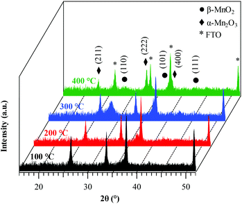 | ||
| Fig. 1 XRD patterns of the target manganese oxide samples fabricated at different growth temperatures. Reflections pertaining to β-MnO2, Mn2O3 and FTO substrates are marked for clarity. | ||
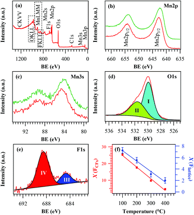
The surface chemical composition of the target systems was analysed using XPS, yielding qualitatively similar results irrespective of the adopted deposition temperature. Survey spectra (Fig. 2a) displayed the presence of C (see also Fig. S1†), O, Mn and F signals. For a growth temperature ≤300 °C, the Mn 2p peak shape and position (Fig. 2b; BE(Mn 2p3/2) = 642.7 eV; spin–orbit splitting = 11.5 eV) were in agreement with the presence of MnO2![[thin space (1/6-em)]](https://www.rsc.org/images/entities/char_2009.gif) 12,17,21,27,31,32 free from other manganese oxides in appreciable amounts, as also confirmed by the Mn 3s multiplet splitting separation (Fig. 2c; 4.7 eV).2,15,18,33,52 In a different way, at 400 °C the Mn 2p spectrum (BE(Mn 2p3/2) = 642.3 eV) and the Mn 3s band spacing (5.4 eV) were in line with the presence of Mn2O3.24,31,40,41 Nevertheless, the energy difference between the BE(Mn 2p3/2) maximum and the O 1s lowest BE component (112.2 eV) was intermediate between those of Mn2O3 and MnO2.10,17,21,25,33
12,17,21,27,31,32 free from other manganese oxides in appreciable amounts, as also confirmed by the Mn 3s multiplet splitting separation (Fig. 2c; 4.7 eV).2,15,18,33,52 In a different way, at 400 °C the Mn 2p spectrum (BE(Mn 2p3/2) = 642.3 eV) and the Mn 3s band spacing (5.4 eV) were in line with the presence of Mn2O3.24,31,40,41 Nevertheless, the energy difference between the BE(Mn 2p3/2) maximum and the O 1s lowest BE component (112.2 eV) was intermediate between those of Mn2O3 and MnO2.10,17,21,25,33
The surface O/Mn atomic ratio (≈1.7–1.5 upon going from 100 °C to 400 °C) was lower than the stoichiometric value for manganese dioxide. The O 1s peak (Fig. 2d) was decomposed by means of two components located at BE = 529.9 eV (I) and 531.6 eV (II). Whereas the former could be assigned to lattice oxygen in the Mn–O–Mn network,6,10,15,24,43 the latter (typically ≈30% of the total O content) was due to the concurrence of hydroxyl groups and atmospheric oxygen adsorbed onto surface defect sites.9,16,30,33,59 Non-stoichiometric O vacancy-rich β-MnO2 is indeed well documented23,37,60 and the presence of “active oxygen” as lattice defects or adsorbed species onto the surface has been reported to enhance its catalytic activity in various processes.15,24,33,37,38 This feature favourably impacts even on the system photocatalytic performances, as discussed in detail in section 3.2. Finally, the surface F 1s peak (Fig. 2e) was characterized by two components located at BE = 684.9 eV (III) and 688.5 eV (IV). The former, consistent with the presence of lattice F, revealed a successful fluorine incorporation into the oxide lattice due to the used fluorinated precursor in the plasma-assisted processes, leading to F-doped β-MnO2 systems. The second component, related to precursor-derived CFx groups (see also Fig. S1†),49–53 could be removed after Ar+ erosion for 5 min, indicating that its presence was limited to the specimen surface. The uniform in-depth F distribution was confirmed by EDXS analyses (Fig. S2†). As can be observed from Fig. 2f, in line with previous studies,48,50,53 both F components underwent a decrease upon increasing the growth temperature, highlighting the possibility of tailoring F doping in the target MnO2 systems by the sole variation of this parameter.
The nanosystem morphology, investigated by the combined use of FE-SEM and AFM analyses (Fig. 3), revealed a significant dependence on the adopted growth temperature. At 100 °C (Fig. 3a–c), the specimen was characterized by hierarchical dendritic structures (mean lateral dimension = 200 nm; overall deposit thickness = 330 nm) uniformly protruding from the FTO substrate, resulting from the assembly of low-sized lamellar aggregates (length and width = 75 nm and 20 nm, respectively). A similar morphology was obtained even for the sample grown at 200 °C (Fig. 3d–f), although the formation of bigger and denser nanostructures (mean dimension = 230 nm; length and width of the lamellar aggregates = 115 nm and 30 nm, respectively) gave rise to a tightly packed cross-sectional arrangement. In a different way, a net morphological evolution took place for the specimen obtained at 300 °C (Fig. 3g–i), that was characterized by pointed nanothorns (average length and diameter = 900 and 80 nm, respectively; mean aspect ratio = 11.2) protruding from a more compact underlayer ≈300 nm thick. At 400 °C (Fig. 3l–n), the increased thermal energy supply produced more elongated quasi-1D nanostructures (average length and diameter = 900 nm and 50 nm, resulting in an aspect ratio of 18.0), with a thinner underlayer (≈180 nm). The morphology of the 300 °C and 400 °C deposits likely arises from the initial formation on the substrate of a granular layer, subsequently self-catalysing the growth of anisotropic nanothorns in a process assisted by O deficiencies (see the above XPS data), resulting, in turn, from the material bombardment by O-related species.45,52 The surface topography was also probed using AFM, and images recorded on different sample areas enabled ascertaining surface homogeneity. The results, in line with FE-SEM data, confirmed the above discussed morphological evolution, highlighting the formation of highly rough materials. In particular, the calculated RMS roughness values, that can be used as an estimation of surface area,4,7,48 increased exponentially with growth temperature (Fig. S3†), i.e. with decreasing F concentration,47 leading to very high values at 400 °C. Thanks to their open and highly porous morphology, such nanostructures could be deemed to have potential advantages for photocatalytic applications, due to their reduced lateral size and high contact area with the reaction medium.1,3,34,36
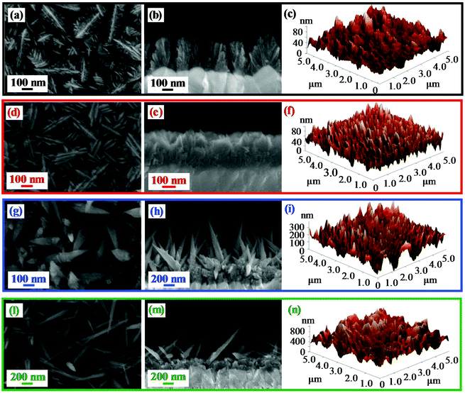 | ||
| Fig. 3 (From left to right) Representative plane-view, cross-sectional FE-SEM images and AFM micrographs of β-MnO2 nanomaterials obtained at different temperatures. | ||
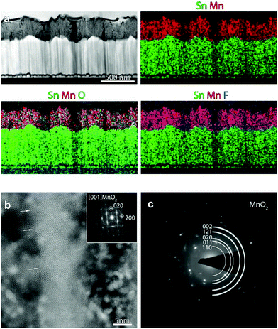
In order to investigate in detail the system structure at the nanoscale, HAADF-STEM and EDXS analyses were carried out on representative specimens fabricated at 200 °C (Fig. 4) and 300 °C (Fig. 5). An overview HAADF-STEM cross-sectional image of the sample grown at 200 °C, together with EDXS elemental maps for Sn, Mn, O and F, is shown in Fig. 4a, revealing the FTO//MnO2 stacking and a homogeneous spatial distribution of the analysed elements. The presence of hierarchical dendritic structures is in line with the results obtained using FE-SEM (compare with Fig. 3). Fig. 4b displays a high resolution HAADF-STEM (Z-contrast) micrograph, together with the fast Fourier transform (FFT) pattern, shown as an inset. The FFT corresponds to the [001] zone axis of the β-MnO2 polymorph, the sole crystalline phase detected in the present specimen, in agreement with XRD results (see above). Many stacking faults could be observed, as indicated by the white arrows in Fig. 4b. SAED analysis (Fig. 4c) highlighted the polycrystalline nature of the target system, as can be noted by the presence of discontinuous circles.
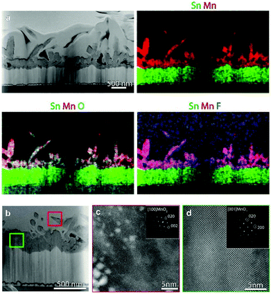
Fig. 5a shows an overview HAADF-STEM image of the specimen grown at 300 °C, along with EDXS elemental maps. The micrographs evidence the assembly of quasi-1D high aspect ratio nanothorns with pointed tips, growing from a relatively compact underlayer in contact with the FTO substrate, in accordance with FE-SEM observations. Fig. 5b shows a higher magnification HAADF-STEM image of a region of the sample, and Fig. 5c and d display representative high resolution HAADF-STEM images for the target nanothorns and the underlayer, collected in the regions marked in Fig. 5b by red and green squares, respectively. The corresponding FFT patterns (insets) reveal that both the nanothorn and underlayer structure correspond to the β-MnO2 polymorph, in agreement with XRD and XPS analyses.
The fabricated materials were also analysed using optical absorption spectroscopy (Fig. 6a). In general, the recorded spectra displayed a prominent radiation absorption in the Vis range, of great importance for photocatalytic applications activated by Vis light (see below). The spectra were also characterized by a broadened absorption tail towards the near-infrared (NIR) region, consistent with the presence of O vacancies (see the above XPS data) and resulting in the formation of sub-band gap states.46,53 From Tauc plots (Fig. 6b), it was possible to extrapolate EG values as 2.5 eV, 2.2 eV, 2.0 eV and 1.8 eV for growth temperatures of 100 °C, 200 °C, 300 °C and 400 °C, respectively. These values were blue-shifted with respect to literature data for MnO2 (typically close to 1.8 eV![[thin space (1/6-em)]](https://www.rsc.org/images/entities/char_2009.gif) 1,13,60,61), a phenomenon that could be ascribed to the occurrence of size effects29,46 and to a modified carrier concentration when oxygen vacancies are saturated by fluorine. This explanation also accounts for the progressive increase of band gap values at the lowest deposition temperatures, resulting in a higher F content (see above and Fig. 2f).47,50,53 For the specimen deposited at 400 °C, the obtained band gap (EG = 1.8 eV) was intermediate between those reported for MnO2 and Mn2O3,3,13,34 in line with the system composition (see above). Fig. 6b also shows that the sample fabricated at 200 °C possesses a higher absorption coefficient (α) with respect to the other ones, a phenomenon traced back to a concurrent favourable contribution of the system crystallinity and the relatively high lattice F content.49 This result is of great importance, since a superior light absorption efficiency positively affects the functional behaviour36 (see below).
1,13,60,61), a phenomenon that could be ascribed to the occurrence of size effects29,46 and to a modified carrier concentration when oxygen vacancies are saturated by fluorine. This explanation also accounts for the progressive increase of band gap values at the lowest deposition temperatures, resulting in a higher F content (see above and Fig. 2f).47,50,53 For the specimen deposited at 400 °C, the obtained band gap (EG = 1.8 eV) was intermediate between those reported for MnO2 and Mn2O3,3,13,34 in line with the system composition (see above). Fig. 6b also shows that the sample fabricated at 200 °C possesses a higher absorption coefficient (α) with respect to the other ones, a phenomenon traced back to a concurrent favourable contribution of the system crystallinity and the relatively high lattice F content.49 This result is of great importance, since a superior light absorption efficiency positively affects the functional behaviour36 (see below).
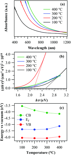 | ||
| Fig. 6 Optical absorption spectra (a) and Tauc plots (b) for manganese oxide samples grown at different temperatures. (c) Schematic band energy diagram of the same specimens. | ||
Fig. 6c displays a schematic band energy diagram reporting conduction band (CB), valence band (VB), and Fermi level (Ef) positions for the various samples. The energy band diagram of manganese oxides is very controversial in the literature, not only due to complications arising from the large number of possible polymorphs, but also because of the complex influence of oxygen-related defects, grain boundaries and, in the present case, also of fluorine doping.19,37,60,62,63 In this work, the energy diagram in Fig. 6c was sketched based on XPS, KP and optical absorption measurements (see above and Fig. S4†). While the target samples show a rather high conductivity, the results reveal a band structure typical of a semiconductor. Similar to our previous work on F-doped Fe2O3,53 the present data suggest that the increase of band gap values with fluorine content was not due to a Moss–Burstein effect (involving the partial filling of the CB and increase of n-type behaviour with fluorine concentration), but to a different phenomenon, as testified by the progressive increase of the system p-type behaviour at higher F loadings (i.e. lower deposition temperatures). In fact, oxygen vacancies yield occupied sub-band gap states above the VB edge, as suggested by optical absorption data (see above). Due to F incorporation into the material and the subsequent formation of Mn–F bonds (as confirmed by XPS), these states become partially empty and can accept electrons from the MnO2 valence band, generating holes in the latter. This phenomenon is likely to become predominant at higher F concentrations, thus explaining the enhanced p-type character of samples grown at lower temperatures.
3.2 Photoactivated properties
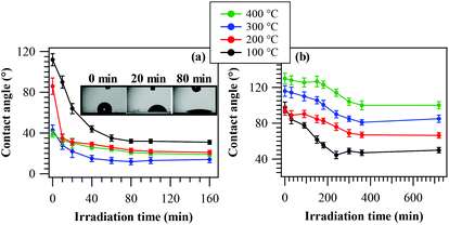
PH tests on the obtained systems were carried out by measuring the evolution of the water contact angle as a function of irradiation time (Fig. 7a). As can be observed, all samples presented a relatively fast variation of their initial state upon UV exposure, yielding appreciably hydrophilic surfaces for sufficiently long irradiation. The typical time within which the final hydrophilic state is reached (<1 h) is in line with previously reported data for other oxide-based materials obtained by CVD and PE-CVD routes.7,8 Nevertheless, the initial WCA value at the beginning of the process (in the absence of UV irradiation) results progressively lower for samples obtained at higher growth temperatures. This feature could be mainly traced back to the different fluorine contents of the target specimens, which, as already discussed, decreases upon increasing the temperature (see Fig. 2f). In fact, the presence of a higher CFx group content on the surface resulted in a more hydrophobic surface,64 as observed for the samples obtained at 100 °C and 200 °C (see also XPS data above). In addition, fluorine presence leads to a passivation of nanomaterial defects and, hence, to a reduced content of oxygen vacancies,48,50,53 the key active sites for water chemisorption, with the formation of new –OH groups.4,7,8,35 As a consequence, higher fluorine loadings result in an increased initial hydrophobicity. An additional concurrent contribution to the trend of the initial contact angles is provided by RMS roughness values, progressively increasing with the growth temperature (Fig. S3†).7,35As can be observed, the system behaviour became more hydrophilic upon irradiation, with a direct dependence on the deposition temperature. The Δ(WCA) value (difference between the initial and final contact angles) is in fact reduced from ≈80 to ≈20° upon going from 100 °C to 400 °C. The rationale for the above difference lies in the different fluorine contents of the target materials, since an increase in F content (at 100 °C) results in an increase of the Lewis acidity of metal centres, beneficially affecting the system activity.49 In addition, at the lowest temperatures, the higher F content is more effective in passivating material defects, thus reducing detrimental electron–hole recombination.53 In a different way, carrier recombination processes are favoured by lower band gap values, indeed corresponding to the less active samples fabricated at higher temperatures. Although for the latter cases an increased RMS roughness would imply a higher active area (see above), it appears that this phenomenon (Fig. S3†) cannot efficiently counterbalance the above effects. In addition, the formation of Mn2O3/MnO2 heterojunctions at 400 °C does not improve the separation of photogenerated charge carriers, due to the unfavourable band edge positions at the interface between these oxides (Fig. S5†). At the end of PH tests, samples were stored in the dark for 12 h and subsequent measurements of initial WCA values revealed the restoring of initial surface characteristics, highlighting the reversibility of the discussed behaviour.
In spite of the preliminary character of these studies, our data highlight that the target nanomaterials are active in photo-induced superhydrophilicity processes and that, in particular, the sample grown at 100 °C exhibited a superior activity with respect to a commercial Pilkington® Activ™ Glass, a reference standard for the target applications.7 These results are of particular interest due to the environmentally friendly character of MnO2 and capability of harvesting solar radiation, differently from TiO2 or ZnO, the most used platforms for such applications.
Solid phase PC performances of the target nanomaterials were examined in the photodecomposition of methyl stearate, a well-known model fatty compound, by monitoring WCA evolution vs. illumination time7 (see the Experimental section; Fig. 7b). As a general rule, the starting WCA values were all higher than 90°, in accordance with the presence of the hydrophobic methyl stearate overlayer. In addition, the initial WCA values progressively increased with the adopted growth temperature. This trend was traced back to the parallel enhancement of the system RMS roughness upon going from 100 °C to 400 °C (see above), a phenomenon which, in turn, increased the system hydrophobicity.7 In general, the material activity resulted directly dependent on the deposition temperature. In particular, the Δ(WCA) value decreased from ≈50° to ≈30° upon going from 100 °C to 400 °C, and even in the latter case the excursion was higher than that exhibited by the reference Pilkington® Activ™ Glass.7 The best performances of the 100 °C-deposited sample could be mainly related to its higher lattice F content (see above and Fig. 2f), exerting a beneficial influence on photocatalytic activity and conductivity and suppressing, in parallel, detrimental electron–hole recombination processes.46,49,51,53 In this case, a predominant contribution of RMS roughness could be ruled out since, as already noted, the corresponding values showed an opposite trend with respect to that shown in Fig. 7b.
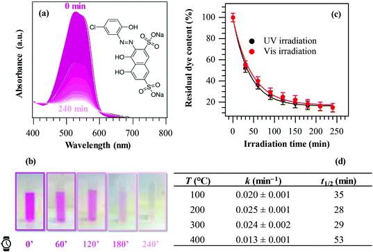
Finally, the liquid phase PC activity of the target specimens was tested in the degradation of Plasmocorinth B aqueous solutions as a function of illumination time. In all cases, control experiments revealed that no dye decomposition took place in the dark and/or in the absence of the target materials. Fig. 8a displays selected optical absorption spectra of the dye solution in the presence of a manganese dioxide specimen, showing a progressive absorbance decrease upon increasing UV irradiation time, and pointing out the effectiveness of these materials to quickly decompose the pollutant. The possible mechanism of the overall process is described in section S-1.5.† The solution fading due to dye degradation is visible also to the naked eye (Fig. 8b). Fig. 8c displays the relative Plasmocorinth B concentration vs. irradiation time in the presence of a representative MnO2 sample. Photocatalytic dye decomposition was carried out utilizing not only UV, but also Vis light. The obtained results (Fig. 8c) revealed a comparable sample activity in both cases (see also kinetic constants and half-life data in Table S1†), an interesting goal from an applicative point of view. In addition, differently from previous studies,42 cyclability tests (Fig. S6†) did not show any significant performance degradation, an issue of vital importance in view of practical applications.4,30,32,56
As a general rule, all specimens were active in the target process and the dye decomposition followed a pseudo-first-order reaction kinetics, as usually reported in similar cases.5,6,34 The values of apparent first-order rate constants and half-life are reported in Fig. 8d. Such results were better than those exhibited in Plasmocorinth B photocatalytic oxidation over supported TiO2 and M/TiO2 (M = Ag, Au) films,36,42,56 thus highlighting the potential of the present materials for use in photocatalytic dye degradation processes.
The obtained data suggest the following trend for the sample photocatalytic activity as a function of the material growth temperature: 400 °C < 100 °C < 300 °C ≈ 200 °C. This trend could be apparently surprising, since the specimen obtained at 400 °C was characterized by the highest RMS roughness (i.e., by a higher active area), and, at a first glance, it could have been expected to be the most active. This result could be explained considering that the system liquid phase photoactivity is affected not only by the actual roughness value, but also by other concurring factors: (i) the different absorption coefficients; (ii) the different lattice F contents; and (iii) the system optical band gaps. In particular, as already observed in relation to data shown in Fig. 7a, lower EG values, corresponding to the samples fabricated at higher temperatures, favour the recombination of photogenerated electrons and holes. In addition, the formation of Mn2O3/MnO2 heterojunctions, occurring for the 400 °C specimen, does not improve charge carrier separation (see also Fig. S5†), due to the unfavourable mutual band edge positions. As a result, taking into account the concomitant effect of the above issues, the most active specimen was the one obtained at a growth temperature of 200 °C.
4. Conclusions
This work has reported the PE-CVD fabrication of MnO2 nanosystems from Ar–O2 plasmas on FTO substrates. The use of a fluorinated Mn(II) molecular precursor enabled a homogeneous F doping of the target systems, with a content directly tuneable as a function of the adopted growth temperature (100–400 °C). Concomitantly, nanosystems with hierarchical morphologies spanning from dendritic structures to quasi-1D sharp nanothorns, with controllable surface roughness and optical properties, could be effectively obtained. The fabricated materials were composed of pure β-MnO2 at a deposition temperature of 100–300 °C, and by the co-presence of β-MnO2 and Mn2O3 at 400 °C. The validity of the proposed preparation route is further highlighted by the fact that, at variance with the preparation of MnO2 polymorphs involving templates and surfactants, it affords high purity products without any post-synthesis treatment, that could alter the desired structures.6 A thorough multi-technique approach enabled the investigation of the interplay between the preparation conditions and the resulting system characteristics. Preliminary photo-induced hydrophilicity/photocatalytic functional tests, both in the solid and in the liquid phase, highlighted the possibility of finely tailoring MnO2 nanomaterial performances, which resulted from a complex interplay between their nano-organization, F content and optical absorption. In addition, the use of Vis illumination instead of UV one did not result in an appreciable performance decrease, paving the way to the use of natural sunlight to activate the target processes. The obtained results, which, to the best of our knowledge, have no precedents to date on the target materials, open challenging perspectives for the development of multi-functional photocatalysts for self-cleaning and antifogging applications, as well as for wastewater treatment.Conflicts of interest
There are no conflicts to declare.Acknowledgements
Padova University DOR 2016–2018, P-DiSC #03BIRD2016-UNIPD projects, the ACTION post-doc fellowship, HERALD Cost Action MP1402 – 37831 and the EPSRC (award EP/R008841/1 and EP/M024938/1) are acknowledged for financial support. T. A. acknowledges a post-doctoral grant from the Research Foundation Flanders (FWO). Thanks are also due to Prof. Sara Bals (EMAT, University of Antwerp, Belgium), Prof. Romana Cerc Korošec and Dr Lev Matoh (University of Ljubljana, Slovenia), and to Prof. Elza Bontempi (Brescia University, Italy).Notes and references
- K. Saravanakumar, V. Muthuraj and S. Vadivel, RSC Adv., 2016, 6, 61357–61366 RSC.
- B. A. Pinaud, Z. B. Chen, D. N. Abram and T. F. Jaramillo, J. Phys. Chem. C, 2011, 115, 11830–11838 CrossRef CAS.
- F. Li, P. Wangyang, A. Zada, M. Humayun, B. Wang and Y. Qu, Mater. Res. Bull., 2016, 84, 99–104 CrossRef CAS.
- S. R. Patil, B. H. Hameed, A. S. Škapin and U. Lavrenčič Štangar, Chem. Eng. J., 2011, 174, 190–198 CrossRef CAS.
- S. Das, A. Samanta and S. Jana, ACS Sustainable Chem. Eng., 2017, 5, 9086–9094 CrossRef CAS.
- A. Baral, D. P. Das, M. Minakshi, M. K. Ghosh and D. K. Padhi, ChemistrySelect, 2016, 1, 4277–4285 CrossRef CAS.
- D. Barreca, A. Gasparotto, C. Maccato, E. Tondello, U. Lavrenčič Štangar and S. R. Patil, Surf. Coat. Technol., 2009, 203, 2041–2045 CrossRef CAS.
- D. Bekermann, A. Gasparotto, D. Barreca, C. Maccato, M. Rossi, R. Matassa, I. Cianchetta, S. Orlanducci, M. Kete and U. Lavrenčič Štangar, Cryst. Growth Des., 2012, 12, 5118–5124 CrossRef CAS.
- W. Tang, M. Yao, Y. Deng, X. Li, N. Han, X. Wu and Y. Chen, Chem. Eng. J., 2016, 306, 709–718 CrossRef CAS.
- F. Gao, X. Tang, H. Yi, C. Chu, N. Li, J. Li and S. Zhao, Chem. Eng. J., 2017, 322, 525–537 CrossRef CAS.
- S. A. Alzahrani, S. A. Al-Thabaiti, W. S. Al-Arjan, M. A. Malik and Z. Khan, J. Mol. Struct., 2017, 1137, 495–505 CrossRef CAS.
- J. Cao, Q. H. Mao, L. Shi and Y. T. Qian, J. Mater. Chem., 2011, 21, 16210–16215 RSC.
- Y. L. Chan, S. Y. Pung, S. Sreekantan and F. Y. Yeoh, J. Exp. Nanosci., 2016, 11, 603–618 CrossRef CAS.
- B. Tang, G. L. Wang, L. H. Zhuo and J. C. Ge, Nanotechnol., 2006, 17, 947–951 CrossRef CAS.
- R. E. John, A. Chandran, M. Thomas, J. Jose and K. C. George, Appl. Surf. Sci., 2016, 367, 43–51 CrossRef CAS.
- M. Sun, B. Lan, T. Lin, G. Cheng, F. Ye, L. Yu, X. L. Cheng and X. Y. Zheng, CrystEngComm, 2013, 15, 7010–7018 RSC.
- J. T. Sampanthar, J. Dou, G. G. Joo, E. Widjaja and L. Q. H. Eunice, Nanotechnol., 2007, 18, 025601 CrossRef.
- G. Cheng, S. Xie, B. Lan, X. Zheng, F. Ye, M. Sun, X. Lu and L. Yu, J. Mater. Chem. A, 2016, 4, 16462–16468 RSC.
- D. M. Robinson, Y. B. Go, M. Mui, G. Gardner, Z. J. Zhang, D. Mastrogiovanni, E. Garfunkel, J. Li, M. Greenblatt and G. C. Dismukes, J. Am. Chem. Soc., 2013, 135, 3494–3501 CrossRef CAS PubMed.
- S. Balamurugan, A. Rajalakshmi and D. Balamurugan, J. Alloys Compd., 2015, 650, 863–870 CrossRef CAS.
- B. S. Singu and K. R. Yoon, J. Alloys Compd., 2017, 695, 771–778 CrossRef CAS.
- A. Kumar, A. Sanger, A. Kumar, Y. Kumar and R. Chandra, Electrochim. Acta, 2016, 220, 712–720 CrossRef CAS.
- J. A. Dawson and I. Tanaka, ACS Appl. Mater. Interfaces, 2014, 6, 17776–17784 CrossRef CAS PubMed.
- J. B. Jia, P. Y. Zhang and L. Chen, Catal. Sci. Technol., 2016, 6, 5841–5847 RSC.
- F. Mattelaer, T. Bosserez, J. Ronge, J. A. Martens, J. Dendooven and C. Detavernier, RSC Adv., 2016, 6, 98337–98343 RSC.
- H.-W. Chang, Y.-R. Lu, J.-L. Chen, C.-L. Chen, J.-F. Lee, J.-M. Chen, Y.-C. Tsai, C.-M. Chang, P.-H. Yeh, W.-C. Chou, Y.-H. Liou and C.-L. Dong, Nanoscale, 2015, 7, 1725–1735 RSC.
- Z. Sun, S. Firdoz, E. Ying-Xuan Yap, L. Li and X. Lu, Nanoscale, 2013, 5, 4379–4387 RSC.
- J. Zhou, H. Zhao, X. Mu, J. Chen, P. Zhang, Y. Wang, Y. He, Z. Zhang, X. Pan and E. Xie, Nanoscale, 2015, 7, 14697–14706 RSC.
- G. A. M. Ali, M. M. Yusoff, E. R. Shaaban and K. F. Chong, Ceram. Int., 2017, 43, 8440–8448 CrossRef CAS.
- C. L. Yu, G. Li, L. F. Wei, Q. Z. Fan, Q. Shu and J. C. Yu, Catal. Today, 2014, 224, 154–162 CrossRef CAS.
- Z. Geng, Y. Wang, J. Liu, G. Li, L. Li, K. Huang, L. Yuan and S. Feng, ACS Appl. Mater. Interfaces, 2016, 8, 27825–27831 CrossRef CAS.
- S. Saha and A. Pal, Sep. Purif. Technol., 2014, 134, 26–36 CrossRef CAS.
- X. P. Li, J. Liu, Y. H. Zhao, H. J. Zhang, F. P. Du, C. Lin, T. J. Zhao and Y. H. Sun, ChemCatChem, 2015, 7, 1848–1856 CrossRef CAS.
- N. Kumar, A. Sen, K. Rajendran, R. Rameshbabu, J. Ragupathi, H. A. Therese and T. Maiyalagan, RSC Adv., 2017, 7, 25041–25053 RSC.
- Y. Yin, R. Huang, W. Zhang, M. Zhang and C. Wang, Chem. Eng. J., 2016, 289, 99–105 CrossRef CAS.
- U. Černigoj, U. Lavrenčič Štangar, P. Trebše, U. O. Krašovec and S. Gross, Thin Solid Films, 2006, 495, 327–332 CrossRef.
- L. Li, X. H. Feng, Y. Nie, S. G. Chen, F. Shi, K. Xiong, W. Ding, X. Q. Qi, J. S. Hu, Z. D. Wei, L. J. Wan and M. R. Xia, ACS Catal., 2015, 5, 4825–4832 CrossRef CAS.
- D. Y. Li, J. Yang, W. X. Tang, X. F. Wu, L. Q. Wei and Y. F. Chen, RSC Adv., 2014, 4, 26796–26803 RSC.
- X.-M. Liu, S.-Y. Fu and C.-J. Huang, Powder Technol., 2005, 154, 120–124 CrossRef CAS.
- J. F. Wang, L. J. Deng, G. Zhu, L. P. Kang, Z. B. Lei and Z. H. Liu, CrystEngComm, 2013, 15, 6682–6689 RSC.
- A. R. Merritt, R. Rajagopalan and J. D. Carter, Thin Solid Films, 2014, 556, 28–34 CrossRef CAS.
- L. Armelao, D. Barreca, G. Bottaro, A. Gasparotto, C. Maccato, E. Tondello, O. I. Lebedev, S. Turner, G. Van Tendeloo, C. Sada and U. Lavrenčič Štangar, ChemPhysChem, 2009, 10, 3249–3259 CrossRef CAS.
- X. J. Xing, Y. P. Yu, L. M. Xu, S. X. Wu and S. W. Li, J. Phys. Chem. C, 2008, 112, 15526–15531 CrossRef CAS.
- S. Islam, M. H. Alfaruqi, V. Mathew, J. Song, S. Kim, S. Kim, J. Jo, J. P. Baboo, D. T. Pham, D. Y. Putro, Y.-K. Sun and J. Kim, J. Mater. Chem. A, 2017, 5, 23299–23309 RSC.
- A. Gasparotto, D. Barreca, D. Bekermann, A. Devi, R. A. Fischer, C. Maccato and E. Tondello, J. Nanosci. Nanotechnol., 2011, 11, 8206–8213 CrossRef CAS.
- N. Haddad, Z. Ben Ayadi, H. Mahdhi and K. Djessas, J. Mater. Sci.: Mater. Electron., 2017, 28, 15457–15465 CrossRef CAS.
- S. Aydogu, M. B. Coban and G. Cabuk, Appl. Phys. A, 2017, 123, 409 CrossRef.
- G. Carraro, D. Barreca, D. Bekermann, T. Montini, A. Gasparotto, V. Gombac, C. Maccato and P. Fornasiero, J. Nanosci. Nanotechnol., 2013, 13, 4962–4968 CrossRef CAS.
- A. Gasparotto, D. Barreca, D. Bekermann, A. Devi, R. A. Fischer, P. Fornasiero, V. Gombac, O. I. Lebedev, C. Maccato, T. Montini, G. Van Tendeloo and E. Tondello, J. Am. Chem. Soc., 2011, 133, 19362–19365 CrossRef CAS.
- G. Carraro, A. Gasparotto, C. Maccato, E. Bontempi, O. I. Lebedev, C. Sada, S. Turner, G. Van Tendeloo and D. Barreca, RSC Adv., 2014, 4, 52140–52146 RSC.
- R. Jin, H. Liu, Y. Guan, J. Zhou and G. Li, CrystEngComm, 2015, 17, 7717–7722 RSC.
- D. Barreca, G. Carraro, E. Fois, A. Gasparotto, F. Gri, R. Seraglia, M. Wilken, A. Venzo, A. Devi, G. Tabacchi and C. Maccato, J. Phys. Chem. C, 2018, 122, 1367–1375 CrossRef CAS.
- D. Barreca, G. Carraro, A. Gasparotto, C. Maccato, C. Sada, A. P. Singh, S. Mathur, A. Mettenbörger, E. Bontempi and L. E. Depero, Int. J. Hydrogen Energy, 2013, 38, 14189–14199 CrossRef CAS.
- P. Schlossmacher, D. O. Klenov, B. Freitag and H. S. von Harrach, Microsc. Today, 2010, 18, 14–20 CrossRef CAS.
- S. Jana, S. Pande, A. K. Sinha, S. Sarkar, M. Pradhan, M. Basu, S. Saha and T. Pal, J. Phys. Chem. C, 2009, 113, 1386–1392 CrossRef CAS.
- L. Armelao, D. Barreca, G. Bottaro, A. Gasparotto, C. Maccato, C. Maragno, E. Tondello, U. Lavrenčič Stangar, M. Bergant and D. Mahne, Nanotechnol., 2007, 18, 375709 CrossRef.
- Pattern No. 024-0735, JCPDS (2000).
- Pattern No. 041-1442, JCPDS (2000).
- M. Liu, G. J. Zhang, Z. R. Shen, P. C. Sun, D. T. Ding and T. H. Chen, Solid State Sci., 2009, 11, 118–128 CrossRef CAS.
- J. Xu, J. B. Liu, B. Huang, S. N. Li and B. X. Liu, Acta Mater., 2017, 131, 88–97 CrossRef CAS.
- M. J. Young, A. M. Holder, S. M. George and C. B. Musgrave, Chem. Mater., 2015, 27, 1172–1180 CrossRef CAS.
- J. A. Dawson, H. Chen and I. Tanaka, ACS Appl. Mater. Interfaces, 2015, 7, 1726–1734 CrossRef CAS.
- Y. Meng, W. Song, H. Huang, Z. Ren, S. Y. Chen and S. L. Suib, J. Am. Chem. Soc., 2014, 136, 11452–11464 CrossRef CAS.
- S. Liu, J. Yu, B. Cheng and M. Jaroniec, Adv. Colloid Interface Sci., 2012, 173, 35–53 CrossRef CAS.
Footnote |
| † Electronic supplementary information (ESI) available: XPS, EDXS and AFM experimental data; KP results; details on photocatalytic tests. See DOI: 10.1039/c8nr06468g |
| This journal is © The Royal Society of Chemistry 2019 |

