Non-layered Ti2N synthesized by plasma process for the anodes of lithium-ion batteries†
Hsu-Sheng
Tsai‡
 *a,
Chih-Hao
Hsu‡
b,
Chong-Chi
Chi
b,
Yi-Chung
Wang
b,
Fan-Wei
Liu
b,
Shin-Yi
Tang
b,
Cho-Jen
Tsai
b,
Hao
Ouyang
b,
Yu-Lun
Chueh
 b and
Jenq-Horng
Liang
*c
aInstitute of Ion Beam Physics and Materials Research, Helmholtz-Zentrum Dresden-Rossendorf, Bautzner Landstraße 400, 01328 Dresden, Germany. E-mail: h.tsai@hzdr.de
bDepartment of Material Science and Engineering, National Tsing Hua Universitry, No. 101, Section 2, Kuang-Fu Road, Hsinchu, Taiwan 30013, Republic of China
cInstitute of Nuclear Engineering and Science, National Tsing Hua Universitry, No. 101, Section 2, Kuang-Fu Road, Hsinchu, Taiwan 30013, Republic of China. E-mail: jhliang@ess.nthu.edu.tw
First published on 15th November 2018
Abstract
Non-layered ε-Ti2N with a work function of ∼4.75 eV, synthesized by a rapid process assisted by N2 plasma immersion, is successfully applied as the anode material of lithium-ion batteries with good performance; it exhibits discharge capacity of ∼450 mA h g−1, which is close to the theoretical value, coulombic efficiencies of >85%, and capacity retentions (≥80%).
As the field of two-dimensional (2D) materials, mostly defined as layer-structured crystals with interlayered van der Waals force, was pioneered by graphene,1 other elemental analogs2 and binary transition metal dichalcogenides (TMDs)3 were extensively investigated during the last decade sequentially. Recently, a new family of 2D materials, so-called MXenes, acquired from MAX phases by selective chemical etching using HF aqueous solution, has been announced by Gogotsi et al.4 The MAX ceramics are composed of an early transition metal (M), an element of group IIIA or IVA (A), and carbon and/or nitrogen(X) with stoichiometric ratios of n + 1, 1, and n (n = 1, 2, or 3), respectively. MXenes are the remaining part of MAX crystals after the removal of A layers. In this review article,4 it is mentioned that the selective etching method can only be feasible for obtaining carbon- and carbonitride-based MXenes from Tin+1AlCn and Ti3AlCN, respectively, but not for obtaining nitride-based ones from Tin+1AlNn. The calculated cohesive energies of nitride-based MXenes are relatively lower, implying that the crystal structure is unstable. In addition, the formation energies of MXenes obtained from Tin+1AlNn are higher, indicating stronger bonding of Al atoms (A layers) in Tin+1AlNn. Hence, the real applications of MXenes are restricted to carbon- and carbonitride-based materials so far.
In 2017, the MXene phase of Ti2N obtained by the etching of KF-HCl mixed solution for the application of surface-enhanced Raman scattering (SERS) was claimed by Soundiraraju et al.5 However, the analytical results were not strong enough to identify that the material acquired by them is hexagonal Ti2N with the space group of P63/mmc. On the other hand, first-principles have been utilized to predict the phase stability of Ti2N under pressure.6 Surprisingly, hexagonal Ti2N with the space group of P63/mmc is the most unstable phase among the 16 crystal structures according to calculations.6 Moreover, it is not included in the Ti–N phase diagram under atmospheric pressure, whereas the Ti–C binary system contains the Ti2C phase with a trigonal lattice equivalent to the hexagonal one.7,8 Actually, Eibler has already theoretically investigated the electronic structures of ε- and δ′-Ti2N in 1993, which are the most stable phases of Ti2N.9 The report indicated that the metastable tetragonal δ′-Ti2N phase with long-range order defects can be formed by annealing TiNx (0.5 < x < 0.6) samples, which might be prepared by introducing N atoms into α-Ti under a particular process at 773 K. After aging, δ′-Ti2N can spontaneously transform into the stable ε-Ti2N phase with the anti-rutile structure, as shown in Fig. 1. ε-Ti2N can also be directly obtained by heating δ-TiN0.5 crystals at a temperature of ∼900 K.
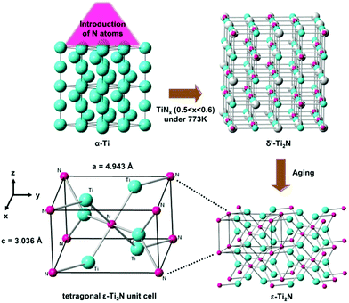 | ||
| Fig. 1 An illustration of phase transformation from α-Ti to ε-Ti2N under particular conditions. Cyan spheres: Ti atoms. Pink spheres: N atoms. Gray spheres: N vacancies. | ||
Although it may not be possible to use nitride-based MXenes for practical applications, computational studies were still conducted by some groups to evaluate their potential for real devices, especially ion batteries. The 2D hexagonal Ti2N monolayer and its terminated derivatives Ti2NT2 (T = O, F, and OH) as the anode materials of different ion batteries were theoretically studied by Wang et al.10 Particularly, the much higher Mg2+ capacity (∼3000 mA h g−1) of the hexagonal Ti2N monolayer due to the two-electron reaction and the unique adsorption behavior was highlighted in the article. Its Li+ capacity could probably reach 487 mA h g−1 under a low open-circuit voltage (OCV) due to the low energy barrier of 0.015 eV for Li+ diffusion.11 In this study, we stably synthesized a non-layered ε-Ti2N thin film assisted by N2 plasma treatment and experimentally demonstrated its potential to be used as an anode material of lithium-ion batteries (LIBs).
The Ti thin film with thickness of ∼20 nm was first deposited on a 2-inch sapphire wafer by a direct current (DC) sputtering system. The deposition time was 2 minutes, and the substrate was kept at room temperature. The working pressure and the DC power were 1 mTorr and 90 W, respectively. Then, the Ti thin film on sapphire was exposed to N2 plasma produced by a radio frequency (RF) (13.56 MHz) system with a power of 100 W under ∼10−1 Torr for 15–60 minutes. The plasma immersion was followed by an annealing process with a temperature of 800 °C under N2/H2 (6/1, v/v) ambiance for 30 minutes.
Kelvin probe force microscopy (KPFM) of the peak force mode in the atomic force microscope (AFM, Bruker, Dimension Icon) was employed to measure the work function of the as-synthesized titanium nitride for initial confirmation of the stoichiometric ratio. The surface composition was analyzed by an X-ray photoelectron spectrometer (XPS, Ulvac-PHI, Versaprobe II) to characterize the bonding configuration. The spherical-aberration corrected transmission electron microscope (TEM, JEOL, JEM-ARM200FTH) with 0.1 nm resolution of the lattice image and 200 kV accelerated voltage was utilized to monitor the crystal structure under nanoscale.
The ε-Ti2N thin film was synthesized on a 0.3 μm-Cu foil instead of sapphire for the following application of LIBs. It was examined by using the 2032 coin cells with metallic lithium as the counter electrode in an argon-filled glove box (MBraun Labmaster 130). The electrolyte used for the half cells was 1 M-LiPF6 in a 50![[thin space (1/6-em)]](https://www.rsc.org/images/entities/char_2009.gif) :
:![[thin space (1/6-em)]](https://www.rsc.org/images/entities/char_2009.gif) 50 (w/w) mixture of ethylene carbonate (EC) and diethyl carbonate (DEC). The cycle performance, rate capacity, and cyclic voltammetry (CV) were measured by the galvanostatic method within the voltage range between 0.01 and 1.5 V. The scanning rate was 0.1 mV s−1 for the CV measurement.
50 (w/w) mixture of ethylene carbonate (EC) and diethyl carbonate (DEC). The cycle performance, rate capacity, and cyclic voltammetry (CV) were measured by the galvanostatic method within the voltage range between 0.01 and 1.5 V. The scanning rate was 0.1 mV s−1 for the CV measurement.
The Kelvin probe force microscopy (KPFM) mappings of the samples after our processes with different plasma exposure times are shown in Fig. 2. Au was used as the reference to first measure the average difference of the work function (ϕd) between Au and the probe. The work function of Au (ϕAu) has been known to be 5.1 eV and hence, that of the probe (ϕp) could be obtained for deriving those of the as-synthesized materials (ESI†). As can be seen in Fig. 2, the values of their work functions are all within the range of 4.7–4.8 eV, implying that Ti2N is successfully synthesized by our method.12 Although the crystal structure of Ti2N, whose work function is theoretically predicted by Liu et al.,12 is hexagonal with the space group of P63/mmc, the work functions of materials with identical chemical formulas are not altered significantly with lattice structure unless the valence electron concentration is changed. Among all the conditions, the uniformity of Ti2N formed by the process with a plasma exposure time of 30 minutes is the best, as shown in Fig. 2. Therefore, the exposure time of plasma is fixed at 30 minutes in the process of synthesizing Ti2N for the following application of LIBs.
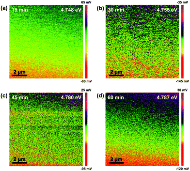 | ||
| Fig. 2 The KPFM images of the titanium nitride synthesized with N2 plasma exposure times of (a) 15, (b) 30, (c) 45, and (d) 60 minutes. | ||
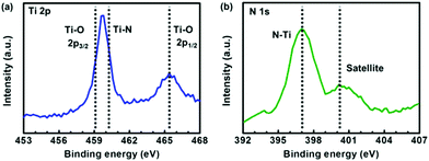
The Ti 2p and N 1s X-ray photoelectron spectroscopy (XPS) spectra of Ti2N synthesized by the process with N2 plasma treatment for 30 minutes were surveyed to realize the chemical bonding configuration. The Ti–O peak splitting into 2p3/2 (∼459.1 eV) and 2p1/2 (∼465.2 eV) bands is associated with inevitable oxygen contamination under atmosphere, as shown in Fig. 3a.13,14 The Ti–N peak located at ∼460.2 eV is partially overlapped by the Ti–O 2p3/2 peak, indicating that the compound of titanium and nitrogen is formed.13,14 In Fig. 3b, the N–Ti peak can be clearly observed at the position of ∼397.0 eV, and the satellite peak emerging at ∼400.1 eV is ascribed to an abrupt change in the effective charge as a core electron is removed due to photoionization. It is worth noting that the discrepancy between our XPS results and those reported in ref. 5 is not significant and within the uncertainty range, indicating that the crystal structure of Ti2N might not be accurately recognized only by XPS analysis. As a result, further structure identification of materials is necessary to confirm the lattice type of Ti2N obtained by our synthesis.
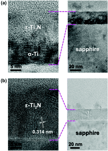
The substantial crystal structure of Ti2N synthesized with the assistance of N2 plasma immersion was identified by transmission electron microscopy (TEM) observation. Fig. 4a shows the cross-sectional TEM image of the sample manufactured by our process with a plasma exposure time of 15 minutes. It is apparent that there is a bilayer structure on the sapphire substrate. Under high magnification, the α-Ti layer covered by ε-Ti2N can be clearly observed, suggesting that the plasma exposure time is too short to fill the whole α-Ti thin film with sufficient nitrogen ions via diffusion. Imaginably, the amount of nitrogen element tends to be enough for the entire formation of ε-Ti2N from α-Ti as the plasma exposure time is increased. The polycrystalline ε-Ti2N thin film on sapphire is completely transformed from α-Ti after N2 plasma treatment for 30 minutes followed by annealing, as shown in the TEM image of Fig. 4b. The distance of ∼0.314 nm labeled in Fig. 4b corresponds to the lattice constant of 3.036 Å (Fig. 1) with a reasonable error range of <5%, indicating that it is the interplanar spacing of (001). Undoubtedly, α-Ti should entirely transform into ε-Ti2N after the process with longer plasma exposure time (Fig. S1, ESI†). Nevertheless, thin film uniformity can become worse due to excess physical bombardment, which is manifested by the results of KPFM.
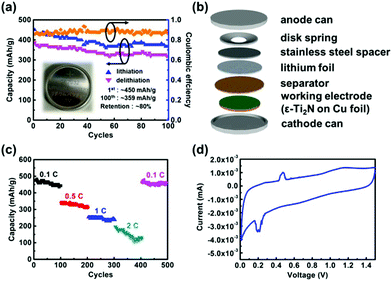
After the material analysis was accomplished, ε-Ti2N thin films were synthesized on Cu foil for fabrication of half cells to evaluate the feasibility for use as the anode materials of LIBs. The discharge–charge (lithiation–delithiation) capacities of the ε-Ti2N thin film are exhibited in Fig. 5a with an inset of the photo of a coin cell, in which the components and their stacking sequence are illustrated in Fig. 5b. The discharge capacity of ∼450 mA h g−1, which is comparable with the theoretical value reported in ref. 11, can be achieved, and the charge capacity can reach ∼387 mA h g−1 in the first cycle such that the initial coulombic efficiency is around 86%. The retentions of the discharge and charge capacities are ∼80 and ∼82%, respectively, even if the 100th cycle is approached, revealing good performance of the cell. The capacities can be maintained with the number of cycles since the crystal structure of ε-Ti2N might not change significantly during the lithiation–delithiation procedure. Consequently, the ε-Ti2N material possesses quite high potential to be used as the anode material for the application of LIBs.
We further measured the performance of Ti2N electrode under different C-rates (0.1, 0.5, 1, 2, and 0.1C) for 500 cycles and the period of each current density was 100 cycles to observe the cycle performance for battery life. The 0.1C-rate is used for the first 100 cycles, which delivers a capacity of 450 mA h g−1, as shown in Fig. 5c. The capacity gradually decreases with increasing C-rate, which is related to diffusion dynamics. The values of the capacities at the 200th, 300th, and 400th cycles are ∼315, ∼240, and ∼120 mA h g−1, respectively. It is noted that the capacity clearly decreases and the coulombic efficiency remains only ∼50% as the 2C-rate is reached (301–400 cycles), implying that the rapid loss of capacity is due to structural damage caused by volume expansion. This phenomenon on anode materials is a common issue and should be overcome for the practical use of LIBs. When the current density is returned to 0.1C-rate, the capacity of ∼450 mA h g−1, which is nearly the same as that of the first 100 cycles, is obtained, and the coulombic efficiency remains above 85%. It is suggested that ε-Ti2N can retain its original electrochemical behavior after undergoing a series of cycles with different C-rates. As a result, it is a potential candidate to be used as an anode material of batteries.
Cyclic voltammetry (CV) can be utilized to observe the behavior of the electrochemical reaction between lithium ions and ε-Ti2N. Fig. 5d shows the oxidation and reduction curves of ε-Ti2N during the first cycle. A quite weak reduction peak first emerging at ∼0.25 V under the reduction current might represent the formation of solid electrolyte interphase (SEI). As the voltage keeps decreasing, an overlapped reduction peak at ∼0.22 V possibly originating from the formation of Li5TiN3 and/or Li2TiN2 can be observed, indicating the occurrence of an electrochemical reaction between lithium ions and ε-Ti2N.15 At last, the reduction peak at ∼0.02 V might result from the formation of Li3N.15 This is the main reaction between lithium ions and ε-Ti2N. On the other hand, there is an oxidation peak at ∼0.5 V, which might be induced by the extraction of lithium ions from Li3N under the oxidation current.15 According to the CV curve, the polarization effect of ε-Ti2N is not clear during the discharge–charge process. Therefore, it is suitable for the applications of LIBs.
Conclusions
In conclusion, in this study, we developed a rapid process assisted by N2 plasma exposure to synthesize a tetragonal ε-Ti2N thin film, which is actually the most stable phase of Ti2N rather than the hexagonal one; also, we demonstrated the good capacity retentions (≥80%) of LIBs fabricated by using it as the anode. According to the results of material analysis, ε-Ti2N, having work function between 4.7 and 4.8 eV, is formed via the reaction between α-Ti thin film and nitrogen ions introduced by plasma immersion under annealing. The discharge and charge capacities of LIBs in the first cycle are ∼450 and ∼387 mA h g−1, respectively. Furthermore, the initial coulombic efficiency is higher than 85% and then, it gradually increases with the number of cycles to ∼88.9% until the 100th cycle. Eventually, it is worth noting that a potential candidate of the anode material of LIBs, ε-Ti2N, was stably synthesized by a low-cost process.Conflicts of interest
There are no conflicts to declare.Notes and references
- K. S. Novoselov, A. K. Geim, S. V. Morozov, D. Jiang, Y. Zhang, S. V. Dubonos, I. V. Grigorieva and A. A. Firsov, Science, 2004, 306, 666 CrossRef CAS PubMed.
- H. S. Tsai and J. H. Liang, ChemNanoMat, 2017, 3, 604 CrossRef CAS.
- S. Z. Butler, S. M. Hollen, L. Cao, Y. Cui, J. A. Gupta, H. R. Gutiérrez, T. F. Heinz, S. S. Hong, J. Huang, A. F. Ismach, E. Johnston-Halperin, M. Kuno, V. V. Plashnitsa, R. D. Robinson, R. S. Ruoff, S. Salahuddin, J. Shan, L. Shi, M. G. Spencer, M. Terrones, W. Windl and J. E. Goldberger, ACS Nano, 2013, 7, 2898 CrossRef CAS PubMed.
- M. Naguib, V. N. Mochalin, M. W. Barsoum and Y. Gogotsi, Adv. Mater., 2014, 26, 992 CrossRef CAS PubMed.
- B. Soundiraraju and B. K. George, ACS Nano, 2017, 11, 8892 CrossRef CAS PubMed.
- V. I. Ivashchenko, P. E. A. Turchi, V. I. Shevchenko and E. I. Olifan, Phys. Rev. B: Condens. Matter Mater. Phys., 2012, 86, 064109 CrossRef.
- H. A. Wriedt and J. L. Murray, Bull. Alloy Phase Diagrams, 1987, 8, 378 CrossRef CAS.
- K. J. Cai, Y. Zheng, P. Shen and S. Y. Chen, CrystEngComm, 2014, 16, 5466 RSC.
- R. Eibler, J. Phys.: Condens. Matter, 1993, 5, 5261 CrossRef CAS.
- D. Wang, Y. Gao, Y. Liu, D. Jin, Y. Gogotsi, X. Meng, F. Du, G. Chen and Y. Wei, J. Phys. Chem. C, 2017, 121, 13025 CrossRef CAS.
- H. Pan, J. Mater. Chem. A, 2015, 3, 21486 RSC.
- Y. Liu, H. Xiao and W. A. Goddard, J. Am. Chem. Soc., 2016, 138, 15853 CrossRef CAS PubMed.
- J. C. Pivin, F. Pons, J. Takadoum, H. M. Pollock and G. Farges, J. Mater. Sci., 1987, 22, 1087 CrossRef CAS.
- E. Galvanettoa, F. P. Gallianoa, F. Borgiolia, U. Bardib and A. Lavacchi, Thin Solid Films, 2001, 384, 223 CrossRef.
- Y. Zhu, X. He and Y. Mo, Adv. Sci., 2017, 4, 1600517 CrossRef PubMed.
Footnotes |
| † Electronic supplementary information (ESI) available. See DOI: 10.1039/c8qi01105b |
| ‡ These authors contributed equally to this work. |
| This journal is © the Partner Organisations 2019 |

