Enhanced intramolecular charge transfer of unfused electron acceptors for efficient organic solar cells†
Ran
Qin‡
 a,
Weitao
Yang‡
a,
Shuixing
Li
a,
Tsz-Ki
Lau
b,
Zhipeng
Yu
a,
Zhang
Liu
a,
Minmin
Shi
a,
Weitao
Yang‡
a,
Shuixing
Li
a,
Tsz-Ki
Lau
b,
Zhipeng
Yu
a,
Zhang
Liu
a,
Minmin
Shi
 a,
Xinhui
Lu
 *b,
Chang-Zhi
Li
 *a and
Hongzheng
Chen
 *a
*a
aMOE Key Laboratory of Macromolecular Synthesis and Functionalization, State Key Laboratory of Silicon Materials, Department of Polymer Science and Engineering, Zhejiang University, Hangzhou 310027, P. R. China. E-mail: hzchen@zju.edu.cn; czli@zju.edu.cn
bDepartment of Physics, Chinese University of Hong Kong, New Territories, P. R. China. E-mail: xhlu@phy.cuhk.edu.hk
First published on 18th January 2019
Abstract
It is promising, yet challenging, to employ molecules of slight synthetic complexity to construct efficient and low-cost organic solar cells (OSCs). Herein, two unfused acceptors, DF-TCIC and HF-TCIC, were developed for OSC applications, in which the 3,4-difluorothiophene core connected through a cyclopentadithiophene (CPDT) bridge to 1,1-dicyanomethylene-3-indanone derivatives (IC for DF-TCIC and DFIC for HF-TCIC, respectively). As mediated by intramolecular non-covalent interactions, these unfused acceptors exhibited a nearly planar structure, and a strong charge transfer effect. HF-TCIC-based OSCs showed a high short-circuit current density (Jsc) of 20.04 mA cm−2 and a power conversion efficiency (PCE) of 9.86%, thereby outperforming DF-TCIC-based devices (Jsc of 16.39 mA cm−2 and PCE of 8.23%). This work suggests that unfused acceptors of slight synthetic complexity are promising for OSC applications.
Introduction
Organic solar cells (OSCs) have drawn the widespread attention of researchers due to their lightweight and flexible features stemming from organic and polymeric materials. In recent years, fast progress on OSC development based on material innovation has been made. For instance, fused-ring electron acceptors (FREAs)1–8 show advantages of adjustable optoelectronic properties to pair with various donors,9–15 resulting in performance improvement16–22 and record power conversion efficiencies (PCEs) of more than 14% and 17% for single-junction23 and tandem OSCs,24 respectively. Among three parameters (i.e., open circuit voltage, Voc, short circuit current density, Jsc and fill factor, FF) to determine device PCE values, the improvement of Jsc arises from the enhanced photon unitization of OSCs on the overall available solar spectra.25–27 At present, the major high-performance FREAs in single-junction OSCs have their absorption onsets at ∼800 nm, with the best device Jsc values only slightly over 20 mA cm−2.23,28 However, assuming complete photon-to-electron conversion of 280–900 nm of the solar spectrum, the highest current density can be 29.8 mA cm−2,29 wherein high performance can be expected without losing too much device voltage. Moreover, Jsc of OSCs can further correlate with the absorption coefficient and absorption range of active components, as well as their charge mobilities, which are determined by the structural factors of organic semiconductors.Conversely, with the PCE of OSCs approaching practical thresholds, consideration of new molecules that are not synthetically complex should also be valuable30 because the number of synthetic and purification steps for organic semiconductors is linked directly to the material costs of OSCs. In this regard, although exhibiting high efficiencies in OSCs, some acceptors need multiple steps of synthesis, which can hinder commercial perspectives. Bearing this in mind, we investigated new molecular design strategies for electron acceptors of simple structure and few synthetic complexities. Our research team has recently developed a series of small-molecule acceptors possessing an unfused central core.31–34 With the assistance of non-covalent interaction, such acceptors allow maintenance of a nearly planar backbone while exhibiting the advantages of easy synthesis from commercial materials.35–39 However, one drawback is that the unfused acceptor DF-PCIC showed a moderate Jsc of 15.66 mA cm−2 for an absorption onset of 781 nm.31 To improve the Jsc of such OSCs, we sought to extend the absorption range of this type of unfused molecule by enhancing the ICT effect between electron-withdrawing and electron-donating moieties.40–44 Besides, investigation of the structure–property correlation of such unfused non-fullerene acceptors would be interesting for accessing simple and effective active molecules for practical OSCs.45,46
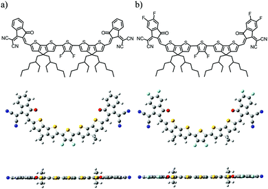
Herein, we designed and synthesized two new electron acceptors, DF-TCIC and HF-TCIC, wherein the 3,4-difluorothiophene core connected, through a cyclopenta[2,1-b:3,4-b′]dithiophene (CPDT) bridge, to the end groups of 1,1-dicyanomethylene-3-indanone derivatives (IC for DF-TCIC and DFIC for HF-TCIC, respectively). As shown in Fig. 1, both acceptors adopted a planar molecular geometry with the assistance of non-covalent interaction. The DFIC group with strong-electron withdrawing capability facilitated HF-TCIC with an enhanced ICT effect and more ordered arrangement in films compared with those of DF-TCIC with an IC group. In addition, HF-TCIC exhibited increased electron mobility in devices over that of DF-TCIC. Therefore, HF-TCIC-based inverted devices with PBDB-T polymers showed the best efficiency of 9.86% with an increased Jsc of 20.04 mA cm−2, whereas the Jsc and PCE of DF-TCIC-based devices was 16.39 mA cm−2 and 8.23%, respectively. An improvement of >20% in the Jsc compensated for the slightly decreased Voc, resulting in an overall improvement of efficiency for HF-TCIC-based devices. This work indicated that the design of simple and unfused acceptors would also be promising for realizing efficient OSCs.
Results and discussion
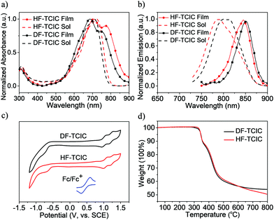
The detailed synthetic procedures of DF-TCIC and HF-TCIC are described in the ESI.† The raw materials, 4,4-bis(2-ethylhexyl)-4H-cyclopenta[2,1-b:3,4-b′]dithiophene (CPDT) and 3,4-difluoro-2,5-bis-trimethylstannanylthiophene, are available commercially. The chemical structures of DF-TCIC and HF-TCIC were confirmed by 1H nuclear magnetic resonance (NMR), 13C NMR, 19F NMR and matrix-assisted laser desorption/ionization time of flight (MALDI-TOF) mass spectroscopy. To investigate the molecular geometry of two new acceptors, a density functional theory (DFT) calculation was carried out (Fig. 1 and Fig. S1, ESI†). Both acceptors possessed a nearly planar structure. The dihedral angles between CPDT and 3,4-difluorothiophene were only 0.02° for DF-TCIC and 0.01° for HF-TCIC, which could be explained by the F–H non-covalent interaction between 3,4-difluorothiophene and CPDT units.UV-vis spectroscopy (Table 1, Fig. 2a and Fig. S2a, ESI†) was employed to study the optical properties of the two molecules. For DF-TCIC, one absorption peak appeared at 711 nm in chloroform solution, and the absorption spectrum was broadened at film state with two peaks at 686 nm and 746 nm, respectively. These features could be ascribed to the enhanced molecular aggregation from solution to film state. With regard to HF-TCIC, due to the stronger electron-withdrawing ability of fluorine atoms, its ICT effect was enhanced and, accordingly, the absorption onset in both solution and film showed a red-shift over those of DF-TCIC. One main peak appeared at 724 nm for HF-TCIC solution and two peaks could be found at 706 nm and 772 nm for film. In addition, compared with DF-TCIC, HF-TCIC exhibited stronger shoulder peaks, indicating intensified intermolecular stacking in the film state. From the absorption onsets at 850 nm for DF-TCIC and 861 nm for HF-TCIC, the optical bandgaps were calculated to be 1.46 eV (DF-TCIC) and 1.44 eV (HF-TCIC). In addition, the photoluminescence (PL) emission spectra of DF-TCIC and HF-TCIC in chloroform solution and films were obtained (Fig. 2b and Fig. S2b, ESI†). In the film state, the PL emission peaks of DF-TCIC and HF-TCIC were at 846 nm and 851 nm, respectively. The corresponding Stokes shift between the maximum absorption and emission peaks of DF-TCIC was 0.34 eV, whereas it was 0.30 eV for HF-TCIC. The smaller Stokes shift indicated a decreased molecular reorganization energy of HF-TCIC in film compared with that of DF-TCIC. The electrochemical properties of the two molecules was characterized by cyclic voltammetry (CV) measurements and their energy levels are shown in Fig. 2c. The equation ELUMO/HOMO = −e(Ered/ox + 4.36) (eV) was used to calculate the lowest unoccupied molecular orbital (LUMO) and highest occupied molecular orbital (HOMO) levels because in our research team the redox potential of Fc/Fc+ was measured to be 0.44 V (the energy level of Fc/Fc+ as 4.80 eV below a vacuum). Then, the onset reduction potential (Ered) and onset oxidation potential (Eox) were found to be −0.60/1.01 V for DF-TCIC, and −0.53/1.07 V for HF-TCIC. Thus, the LUMO/HOMO values were −3.76/−5.37 eV for DF-TCIC, and −3.83/−5.43 eV for HF-TCIC, respectively. Due to the introduction of two more fluorine atoms onto end groups, HF-TCIC exhibited slightly deeper energy levels than those of DF-TCIC. Both acceptors possessed matched energy levels with the polymer donor PBDB-T.
Thermogravimetric analysis (TGA) and differential scanning calorimetry (DSC) were used to investigate the thermal properties of DF-TCIC and HF-TCIC. From Fig. 2d, we can see that the two molecules had a similar thermal decomposition temperature (Td, 5% weight loss) at 345 °C (DF-TCIC) and 344 °C (HF-TCIC) under nitrogen. The DSC curves (Fig. S3, ESI†) revealed that for HF-TCIC, during heating and cooling at 10 °C min−1, obvious melting and crystallization peaks did not appear. With regard to DF-TCIC, only one small melting peak was observed at 253 °C.
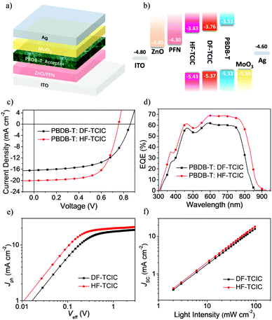
To study the photovoltaic performance of the two molecules in OSCs, we employed the wide-bandgap polymer, PBDB-T, as an electron donor to pair with these acceptors in an inverted-device architecture:indium tin oxide (ITO)/ZnO/poly[9,9-bis(3′-(N,N-dimethylamino)propyl)-2,7-fluorene)-alt-2,7-(9,9-ioctylfluorene] (PFN)/PBDB-T:acceptor/MoO3/Ag. The device structure and energy-level diagram are shown in Fig. 3a and b, respectively. With an optimal weight ratio of donor![[thin space (1/6-em)]](https://www.rsc.org/images/entities/char_2009.gif) :
:![[thin space (1/6-em)]](https://www.rsc.org/images/entities/char_2009.gif) acceptor at 1
acceptor at 1![[thin space (1/6-em)]](https://www.rsc.org/images/entities/char_2009.gif) :
:![[thin space (1/6-em)]](https://www.rsc.org/images/entities/char_2009.gif) 1.2, DF-TCIC and HF-TCIC exhibited the best efficiencies upon addition of 0.5% 1-chloronaphthalene (CN) and appropriate thermal annealing of blend film (140 °C for DF-TCIC blends and 120 °C for HF-TCIC blends). The data and J–V curves of the devices are summarized in Table 2 and Fig. 3c, respectively. HF-TCIC-based OSCs showed an increased Jsc and FF over those of DF-TCIC based devices. A device based on a DF-TCIC acceptor achieved a PCE of 8.23%, a Voc of 0.86 V, a Jsc of 16.39 mA cm−2 and a FF of 0.58. Due to the broad absorption range of HF-TCIC, the Jsc of a HF-TCIC-based device was improved to 20.04 mA cm−2. In addition, the FF was increased to 0.65. As a result, an improved PCE of 9.86% was obtained. The external quantum efficiency (EQE) spectra are presented in Fig. 3d, and reveal that HF-TCIC-based devices possessed a broader and stronger response than DF-TCIC-based devices. These data are consistent with the higher Jsc of HF-TCIC-based devices. The integral current densities (Jcal.) calculated from the EQE curves were also in good agreement with the Jsc.
1.2, DF-TCIC and HF-TCIC exhibited the best efficiencies upon addition of 0.5% 1-chloronaphthalene (CN) and appropriate thermal annealing of blend film (140 °C for DF-TCIC blends and 120 °C for HF-TCIC blends). The data and J–V curves of the devices are summarized in Table 2 and Fig. 3c, respectively. HF-TCIC-based OSCs showed an increased Jsc and FF over those of DF-TCIC based devices. A device based on a DF-TCIC acceptor achieved a PCE of 8.23%, a Voc of 0.86 V, a Jsc of 16.39 mA cm−2 and a FF of 0.58. Due to the broad absorption range of HF-TCIC, the Jsc of a HF-TCIC-based device was improved to 20.04 mA cm−2. In addition, the FF was increased to 0.65. As a result, an improved PCE of 9.86% was obtained. The external quantum efficiency (EQE) spectra are presented in Fig. 3d, and reveal that HF-TCIC-based devices possessed a broader and stronger response than DF-TCIC-based devices. These data are consistent with the higher Jsc of HF-TCIC-based devices. The integral current densities (Jcal.) calculated from the EQE curves were also in good agreement with the Jsc.
![[thin space (1/6-em)]](https://www.rsc.org/images/entities/char_2009.gif) :
:![[thin space (1/6-em)]](https://www.rsc.org/images/entities/char_2009.gif) DF-TCIC (1
DF-TCIC (1![[thin space (1/6-em)]](https://www.rsc.org/images/entities/char_2009.gif) :
:![[thin space (1/6-em)]](https://www.rsc.org/images/entities/char_2009.gif) 1.2, 0.5% CN, 140 °C) and PBDB-T
1.2, 0.5% CN, 140 °C) and PBDB-T![[thin space (1/6-em)]](https://www.rsc.org/images/entities/char_2009.gif) :
:![[thin space (1/6-em)]](https://www.rsc.org/images/entities/char_2009.gif) HF-TCIC (1
HF-TCIC (1![[thin space (1/6-em)]](https://www.rsc.org/images/entities/char_2009.gif) :
:![[thin space (1/6-em)]](https://www.rsc.org/images/entities/char_2009.gif) 1.2, 0.5% CN, 120 °C) in an inverted structure under illumination of AM 1.5 G at 100 mW cm−2
1.2, 0.5% CN, 120 °C) in an inverted structure under illumination of AM 1.5 G at 100 mW cm−2
| Active layer | V oc (V) | J sc (mA cm−2) | FF | PCEmax (%) | PCEavg (%) |
|---|---|---|---|---|---|
| PBDB-T:DF-TCIC | 0.86 | 16.39 (15.33) | 0.58 | 8.23 | 7.95 |
| PBDB-T:HF-TCIC | 0.76 | 20.04 (18.46) | 0.65 | 9.86 | 9.40 |
To investigate exciton dissociation and charge collection within the devices, a plot of photocurrent (Jph = JL − JD, where JL and JD represent the current density under illumination and darkness, respectively) versus the applied effective voltage (Veff = V0 − Va, where V0 is the voltage at which Jph = 0 and Va is the applied voltage) were measured for DF-TCIC- and HF-TCIC-based devices (Fig. 3e). With increasing Veff, the Jph increased gradually and became saturated when the Veff reached ∼2.3 V (i.e., the charge recombination was at a minimum at a high voltage). The equation Pdiss = Jph/Jsat, where Pdiss is the exciton dissociation probability and Jsat is the saturation photocurrent density, can be used to evaluate the exciton dissociation ability of different devices.47 The Pdiss of HF-TCIC was 94.3%, whereas the Pdiss of DF-TCIC was 93%, which indicated a higher exciton dissociation and charge collection efficiency for the HF-TCIC-based device.
To study the charge-recombination behaviours of devices, the function of Jsc and light density (Plight) is shown in Fig. 3f. The power-law equation Jsc ∝ Pαlight could be applied to describe the relationship between them (where the exponent α represents the extent of bimolecular recombination).47,48 The closer the value of α is to 1, the lower is the probability of bimolecular recombination. The α of the HF-TCIC-based device was 0.98, and was higher than the α for DF-TCIC (0.97). The lower bimolecular recombination usually means more carriers are collected by electrodes instead of recombining, which helps to boost the PCE of devices.
The exciton dissociation and charge transfer were investigated further by PL quenching experiments (Fig. 4a and b). When excited at 600 nm, both emissions of the blend films were quenched effectively, whereas the quenching efficiency of PBDB-T:HF-TCIC (98.0%) was slightly higher than that of PBDB-T:DF-TCIC (96.8%) at 650–900 nm. This result indicated effective charge transfer from PBDB-T to acceptors. When excited at 750 nm, although PL quenching for acceptors was not as effective compared with that of PBDB-T excited at 600 nm, it showed that PBDB-T:HF-TCIC possessed higher quenching efficiency. These data indicated more effective exciton dissociation and charge transfer in a PBDB-T:HF-TCIC film than those of a PBDB-T:DF-TCIC film.
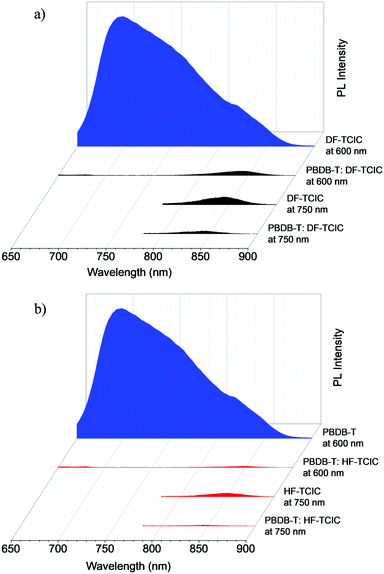 | ||
Fig. 4 PL spectra of a donor PBDB-T film, neat DF-TCIC film, and a blend film of PBDB-T![[thin space (1/6-em)]](https://www.rsc.org/images/entities/char_2009.gif) : :![[thin space (1/6-em)]](https://www.rsc.org/images/entities/char_2009.gif) DF-TCIC (1 DF-TCIC (1![[thin space (1/6-em)]](https://www.rsc.org/images/entities/char_2009.gif) : :![[thin space (1/6-em)]](https://www.rsc.org/images/entities/char_2009.gif) 1.2, 0.5% CN) at (a) 140 °C and (b) 120 °C. 1.2, 0.5% CN) at (a) 140 °C and (b) 120 °C. | ||
The charge-transport properties of devices were also studied by the space charge limited current (SCLC) method (Fig. S4, ESI†). The hole and electron mobility (μh and μe) of blend films were measured. The μh for PBDB-T:DF-TCIC blend films was 8.91 × 10⁻⁵ cm2 V−1 s−1 and the μe was 7.12 × 10⁻⁶ cm2 V−1 s−1. The HF-TCIC-based blend exhibited a μh of 8.33 × 10⁻⁵ cm2 V−1 s−1 and μe of 1.53 × 10⁻⁵ cm2 V−1 s−1, which was about twofold that of μe for DF-TCIC-based blends. Hence, the PBDB-T:HF-TCIC blends possessed a more balanced ratio of μh and μe, which helped to improve the FF for PBDB-T:HF-TCIC blend-based solar cells. Meanwhile, the increase of μe was also an important factor for the improved Jsc, which could be ascribed to enhanced crystallization and π−π stacking due to the introduction of F atoms.
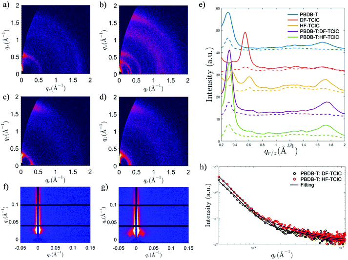
Detailed molecular stacking properties were studied by grazing-incidence wide-angle X-ray scattering (GIWAXS) (Fig. 5 and Fig. S5, ESI†).49 For the DF-TCIC neat film, a strong lamellar peak was located at qz ≈ 0.550 Å−1 along the out-of-plane direction, indicating an “edge-on” orientation of the π-plane in the neat film. Interestingly, the neat HF-TCIC film exhibited a strong π–π stacking peak at qz ≈ 1.72 Å−1, which indicated a preferential “face-on” orientation of molecules. It also showed diffraction peaks at qr ≈ 0.345 Å−1 and 0.615 Å−1, respectively. An extra peak at qr ≈ 0.260 Å−1 might have originated from backbone ordering due to end-group π–π stacking.49 The peaks mentioned above indicated a higher order of molecular arrangement for HF-TCIC.50 For the blend morphology, as shown in Fig. 5e, the two-dimensional GIWAXS patterns of both blends exhibited similar lamellar peaks at qz ≈ 0.315 Å−1. Moreover, π–π stacking was observed at qr ≈ 1.74 Å−1 along the out-of-plane direction, and corresponded to a stacking distance of 3.61 Å, which was similar to that of the pure PBDB-T film. In addition, the π–π stacking peaks of blend films were stronger than those of the pure PBDB-T film. Grazing-incidence small angle X-ray scattering (GISAXS) data were also collected to investigate the domain properties of blend films (Fig. 5f–h and Table S1, ESI†). We adopted the Debye–Anderson–Brumberger (DAB) model and a fractal-like network model to account for the scattering contribution from intermixing amorphous phases and acceptor domains, respectively, by fitting.51 The domain sizes of PBDB-T:DF-TCIC and PBDB-T:HF-TCIC were 9.8 nm and 10.0 nm, respectively. Meanwhile, both blend films showed moderate intermixing phase sizes.
The surface morphologies of blend films were investigated by atomic force microscopy (AFM). The root-mean-square (RMS) surface roughness of PBDB-T:HF-TCIC and PBDB-T:DF-TCIC blend films were 1.66 nm and 3.90 nm, respectively. As shown in Fig. 6, the PBDB-T:HF-TCIC blend film had a less rough and more homogeneous surface. However, a rougher surface and stronger aggregation were observed for the PBDB-T:DF-TCIC blend film.
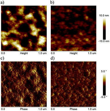 | ||
| Fig. 6 AFM height and phase images of the optimized blend films based on (a) and (c) PBDB-T:DF-TCIC and (b) and (d) PBDB-T:HF-TCIC. | ||
Experimental
Materials
All reagents and solvents, unless specified otherwise, were purchased from J&K Scientific, Suna Tech, Derthon, and Energy Chemical Ltd, and were used without further purification. PBDB-T and PFN-Br were purchased from Solarmer Materials Inc. The detailed synthetic routes are shown in the ESI.†Instrumentation
1H NMR, 13C NMR and 19F NMR spectra were obtained on a Bruker Advance III 400 (400 MHz) NMR system. MALDI-TOF MS spectra were measured on a Walters Maldi Q-TOF Premier machine. UV-vis absorption spectra were recorded on a Shimadzu UV-2450 spectrophotometer. TGA was carried out on a WCT-2 thermal balance under nitrogen protection at a heating rate of 10 °C min−1. DSC was undertaken on a Perkin-Elmer Pyris 1 differential scanning calorimeter. CV curves were created on a CHI600A electrochemical workstation, with a Pt disk, Pt plate, and standard calomel electrode as the working electrode, counter electrode, and reference electrode, respectively, in a 0.1 mol L−1 tetrabutylammoniumhexafluorophosphate (Bu4NPF6) CH2Cl2 solution. Film morphologies were characterized by a VeecoMultiMode AFM system in tapping mode using an etched silicon cantilever at a nominal load of ∼2 nN, and the scanning rate for a 10 μm × 10 μm image size was 1.5 Hz.Fabrication and characterization of devices
OSCs were fabricated on ITO glass substrates with the inverted structure of ITO/ZnO/PFN/active layer/MoO3/Ag. The ITO/glass substrates the ITO/glass substrates were cleaned by sonication using detergent, deionized water, acetone, and isopropanol sequentially for 15 min before fabrication. The pre-cleaned ITO substrates were then treated in an ultraviolet generator for 20 min, followed by deposition of a ZnO thin film by spin-coating precursor solution onto the substrates at 3500 rpm for 60 s and then annealing at 200 °C for 30 min. The ZnO precursor was prepared by dissolving 1 g of zinc acetate dehydrate and 0.3 g of ethanolamine in 10 mL of 2-methoxyethanol. Then, the substrates were transferred into a glovebox, and 0.5 mg mL−1 of ethanol solution of PFN was spin-coated on the ZnO at 3000 rpm for 30 s to form an ultrathin PFN layer. The PBDB-T:HF-TCIC (DF-TCIC) active layer was then spin-coated from 15 mg mL−1 solution (PBDB-T![[thin space (1/6-em)]](https://www.rsc.org/images/entities/char_2009.gif) :
:![[thin space (1/6-em)]](https://www.rsc.org/images/entities/char_2009.gif) HF-TCIC = 1
HF-TCIC = 1![[thin space (1/6-em)]](https://www.rsc.org/images/entities/char_2009.gif) :
:![[thin space (1/6-em)]](https://www.rsc.org/images/entities/char_2009.gif) 1.2 and PBDB-T
1.2 and PBDB-T![[thin space (1/6-em)]](https://www.rsc.org/images/entities/char_2009.gif) :
:![[thin space (1/6-em)]](https://www.rsc.org/images/entities/char_2009.gif) DF-TCIC = 1
DF-TCIC = 1![[thin space (1/6-em)]](https://www.rsc.org/images/entities/char_2009.gif) :
:![[thin space (1/6-em)]](https://www.rsc.org/images/entities/char_2009.gif) 1.2 by wt, dissolved in chloroform with 0.5 vol% 1-chloronaphthalene) at 3500 rpm for 60 s. Subsequently, the devices were annealed at 140 °C (PBDB-T:DF-TCIC) and 120 °C (PBDB-T:HF-TCIC) for 10 min. Finally, a layer of MoO3 (8 nm) and the Ag (100 nm) electrode were deposited by thermal evaporation under a background pressure of ∼5 × 10⁻⁴ Pa.
1.2 by wt, dissolved in chloroform with 0.5 vol% 1-chloronaphthalene) at 3500 rpm for 60 s. Subsequently, the devices were annealed at 140 °C (PBDB-T:DF-TCIC) and 120 °C (PBDB-T:HF-TCIC) for 10 min. Finally, a layer of MoO3 (8 nm) and the Ag (100 nm) electrode were deposited by thermal evaporation under a background pressure of ∼5 × 10⁻⁴ Pa.
The current density–voltage (J–V) curves of the devices were measured in the glovebox with Keithley 2400 measurement source units under 1 sun, AM 1.5 G spectra from a solar simulator (Enlitech), and the light intensity was calibrated with a standard silicon photovoltaic reference cell. EQE spectra were obtained using a Solar Cell Spectral Response Measurement System (QE-R3011; Enlitech).
The charge carrier mobilities of the PBDB-T:DF-TCIC and PBDB-T:HF-TCIC films were measured using the SCLC method. Hole-only devices were fabricated in a structure of ITO/PEDOT:PSS/active layer/MoO3/Ag. Electron-only devices were fabricated in a structure of ITO/ZnO/PFN-Br/active layer/PFN-Br/Ag. Device characteristics were extracted by modelling the dark current under forward bias using the SCLC expression described by the Mott–Gurney law:
GIWAXS and GISAXS measurements
GIWAXS and GISAXS measurements were carried out with a Xeuss 2.0 SAXS/WAXS laboratory beamline using a Cu X-ray source (8.05 keV, 1.54 Å) and a Pilatus3R 300 K detector. The incidence angle was 0.2°.Conclusions
Two new non-fullerene acceptors with unfused central cores were developed by connecting a 3,4-difluorothiophene core, through a CPDT bridge, to IC and DFIC end groups, respectively. With the mediation of non-covalent interactions, these unfused structures exhibited a nearly planar configuration. The stronger ICT effect of HF-TCIC resulted in red-shifted absorption and a narrower bandgap, over those of DF-TCIC. HF-TCIC-based photovoltaic devices showed an improved Jsc of 20.04 mA cm−2 and PCE of 9.86%, compared with DF-TCIC-based devices (Jsc of 16.39 mA cm−2 and PCE of 8.23%). We investigated the structure–property correlations of non-fullerene acceptors with an unfused central core, which suggests that the design of simple and unfused molecular structures allowed improvement in the photovoltaic performances of OSCs.Conflicts of interest
There are no conflicts to declare.Acknowledgements
This research was funded by the National Natural Science Foundation of China (21734008, 21722404, and 21674093), the International Science and Technology Cooperation Program of China (2016YFE0102900), the Ministry of Science and Technology (2017YF0206600) and the Zhejiang Province Science and Technology Plan (2018C01047), and the China Postdoctoral Science Foundation Funded Project (512300-X91706). C.-Z. Li acknowledges the support of the Zhejiang Natural Science Fund for Distinguished Young Scholars (LR17E030001) and the Fundamental Research Funds for the Central Universities. X. L. acknowledges the Research Grant Council of Hong Kong (General Research Fund No. 14314216).References
- Y. Lin, J. Wang, Z.-G. Zhang, H. Bai, Y. Li, D. Zhu and X. Zhan, Adv. Mater., 2015, 27, 1170–1174 CrossRef CAS PubMed.
- J. Hou, O. Inganas, R. H. Friend and F. Gao, Nat. Mater., 2018, 17, 119–128 CrossRef CAS PubMed.
- X. Shi, L. Zuo, S. Jo, K. Gao, F. Lin, F. Liu and A. K.-Y. Jen, Chem. Mater., 2017, 29, 8369–8376 CrossRef CAS.
- T. Li, H. Zhang, Z. Xiao, J. J. Rech, H. Niu, W. You and L. Ding, Mater. Chem. Front., 2018, 2, 700–703 RSC.
- C. Huang, X. Liao, K. Gao, L. Zuo, F. Lin, X. Shi, C.-Z. Li, H. Liu, X. Li, F. Liu, Y. Chen, H. Chen and A. K. Y. Jen, Chem. Mater., 2018, 30, 5429–5434 CrossRef CAS.
- S. Li, Z. Zhang, M. Shi, C.-Z. Li and H. Chen, Phys. Chem. Chem. Phys., 2017, 19, 3440–3458 RSC.
- C. Yan, S. Barlow, Z. Wang, H. Yan, A. K.-Y. Jen, S. R. Marder and X. Zhan, Nat. Rev. Mater., 2018, 3, 18003 CrossRef CAS.
- S. Li, W. Liu, C. Z. Li, M. Shi and H. Chen, Small, 2017, 13, 1701120 CrossRef PubMed.
- W. Liu, J. Zhang, Z. Zhou, D. Zhang, Y. Zhang, S. Xu and X. Zhu, Adv. Mater., 2018, 30, e1800403 CrossRef PubMed.
- C. Sun, F. Pan, H. Bin, J. Zhang, L. Xue, B. Qiu, Z. Wei, Z. G. Zhang and Y. Li, Nat. Commun., 2018, 9, 743 CrossRef PubMed.
- L. Yang, S. Zhang, C. He, J. Zhang, Y. Yang, J. Zhu, Y. Cui, W. Zhao, H. Zhang, Y. Zhang, Z. Wei and J. Hou, Chem. Mater., 2018, 30, 2129–2134 CrossRef CAS.
- D. Liu, J. Wang, C. Gu, Y. Li, X. Bao and R. Yang, Adv. Mater., 2018, 30, 1705870 CrossRef PubMed.
- L. Xue, Y. Yang, J. Xu, C. Zhang, H. Bin, Z. Zhang, B. Qiu, X. Li, C. Sun, L. Gao, J. Yao, X. Chen, Y. Yang, M. Xiao and Y. Li, Adv. Mater., 2017, 29, 1703344 CrossRef PubMed.
- Y. Lin, F. Zhao, S. K. K. Prasad, J. D. Chen, W. Cai, Q. Zhang, K. Chen, Y. Wu, W. Ma, F. Gao, J. X. Tang, C. Wang, W. You, J. M. Hodgkiss and X. Zhan, Adv. Mater., 2018, 30, e1706363 CrossRef PubMed.
- J. Guo, H. Bin, W. Wang, B. Chen, J. Guo, R. Sun, Z.-G. Zhang, X. Jiao, Y. Li and J. Min, J. Mater. Chem. A, 2018, 6, 15675–15683 RSC.
- B. Kan, H. Feng, X. Wan, F. Liu, X. Ke, Y. Wang, Y. Wang, H. Zhang, C. Li, J. Hou and Y. Chen, J. Am. Chem. Soc., 2017, 139, 4929–4934 CrossRef CAS PubMed.
- H. Yao, L. Ye, J. Hou, B. Jang, G. Han, Y. Cui, G. M. Su, C. Wang, B. Gao, R. Yu, H. Zhang, Y. Yi, H. Y. Woo, H. Ade and J. Hou, Adv. Mater., 2017, 29, 1700254 CrossRef PubMed.
- S. Xu, Z. Zhou, W. Liu, Z. Zhang, F. Liu, H. Yan and X. Zhu, Adv. Mater., 2017, 29, 1704510 CrossRef PubMed.
- S. Li, L. Ye, W. Zhao, X. Liu, J. Zhu, H. Ade and J. Hou, Adv. Mater., 2017, 29, 1704051 CrossRef PubMed.
- J. Sun, X. Ma, Z. Zhang, J. Yu, J. Zhou, X. Yin, L. Yang, R. Geng, R. Zhu, F. Zhang and W. Tang, Adv. Mater., 2018, 30, e1707150 CrossRef PubMed.
- Y. Lin, F. Zhao, Q. He, L. Huo, Y. Wu, T. C. Parker, W. Ma, Y. Sun, C. Wang, D. Zhu, A. J. Heeger, S. R. Marder and X. Zhan, J. Am. Chem. Soc., 2016, 138, 4955–4961 CrossRef CAS PubMed.
- W. Liu, S. Li, J. Huang, S. Yang, J. Chen, L. Zuo, M. Shi, X. Zhan, C.-Z. Li and H. Chen, Adv. Mater., 2016, 28, 9729–9734 CrossRef CAS PubMed.
- S. Zhang, Y. Qin, J. Zhu and J. Hou, Adv. Mater., 2018, 30, e1800868 CrossRef PubMed.
- L. Meng, Y. Zhang, X. Wan, C. Li, X. Zhang, Y. Wang, X. Ke, Z. Xiao, L. Ding, R. Xia, H.-L. Yip, Y. Cao and Y. Chen, Science, 2018, 361, 1094–1098 CrossRef CAS PubMed.
- J. Miao, J. Wang, B. Meng, J. Liu and L. Wang, Mater. Chem. Front., 2018, 2, 2333–2339 RSC.
- H. Yao, Y. Cui, R. Yu, B. Gao, H. Zhang and J. Hou, Angew. Chem., Int. Ed., 2017, 56, 3045–3049 CrossRef CAS PubMed.
- Y. Lin, Z.-G. Zhang, H. Bai, J. Wang, Y. Yao, Y. Li, D. Zhu and X. Zhan, Energy Environ. Sci., 2015, 8, 610–616 RSC.
- D. Liu, B. Kan, X. Ke, N. Zheng, Z. Xie, D. Lu and Y. Liu, Adv. Energy Mater., 2018, 8, 1801618 CrossRef.
- E. Bundgaard and F. C. Krebs, Sol. Energy Mater. Sol. Cells, 2007, 91, 954–985 CrossRef CAS.
- J. Roncali, P. Leriche and P. Blanchard, Adv. Mater., 2014, 26, 3821–3838 CrossRef CAS PubMed.
- S. Li, L. Zhan, F. Liu, J. Ren, M. Shi, C.-Z. Li, T. P. Russell and H. Chen, Adv. Mater., 2018, 30, 1705208 CrossRef PubMed.
- S. Li, L. Zhan, W. Zhao, S. Zhang, B. Ali, Z. Fu, T.-K. Lau, X. Lu, M. Shi, C.-Z. Li, J. Hou and H. Chen, J. Mater. Chem. A, 2018, 6, 12132–12141 RSC.
- L. Zhan, S. Li, H. Zhang, F. Gao, T.-K. Lau, X. Lu, D. Sun, P. Wang, M. Shi, C.-Z. Li and H. Chen, Adv. Sci., 2018, 5, 1800755 CrossRef PubMed.
- Z. Zhang, S. Zhang, Z. Liu, Z. Zhang, Y. Li, C.-Z. Li and H. Chen, Acta Phys. – Chim. Sin., 2019, 35, 394–400 Search PubMed.
- Y. Li, X. Liu, F.-P. Wu, Y. Zhou, Z.-Q. Jiang, B. Song, Y. Xia, Z.-G. Zhang, F. Gao, O. Inganas, Y. Li and L.-S. Liao, J. Mater. Chem. A, 2016, 4, 5890–5897 RSC.
- K. Kawashima, T. Fukuhara, Y. Suda, Y. Suzuki, T. Koganezawa, H. Yoshida, H. Ohkita, I. Osaka and K. Takimiya, J. Am. Chem. Soc., 2016, 138, 10265–10275 CrossRef CAS PubMed.
- Y. Liu, Z. Zhang, S. Feng, M. Li, L. Wu, R. Hou, X. Xu, X. Chen and Z. Bo, J. Am. Chem. Soc., 2017, 139, 3356–3359 CrossRef CAS PubMed.
- N. Wang, L. Zhan, S. Li, M. Shi, T.-K. Lau, X. Lu, R. Shikler, C.-Z. Li and H. Chen, Mater. Chem. Front., 2018, 2, 2006–2012 RSC.
- W. Li, L. Ye, S. Li, H. Yao, H. Ade and J. Hou, Adv. Mater., 2018, 30, e1707170 CrossRef PubMed.
- W. Zhao, S. Li, H. Yao, S. Zhang, Y. Zhang, B. Yang and J. Hou, J. Am. Chem. Soc., 2017, 139, 7148–7151 CrossRef CAS PubMed.
- Y. Cui, C. Yang, H. Yao, J. Zhu, Y. Wang, G. Jia, F. Gao and J. Hou, Adv. Mater., 2017, 29, 1703080 CrossRef.
- T. Li, S. Dai, Z. Ke, L. Yang, J. Wang, C. Yan, W. Ma and X. Zhan, Adv. Mater., 2018, 30, 1705969 CrossRef PubMed.
- J. Wang, W. Wang, X. Wang, Y. Wu, Q. Zhang, C. Yan, W. Ma, W. You and X. Zhan, Adv. Mater., 2017, 29, 1702125 CrossRef PubMed.
- N. Liang, W. Jiang, J. Hou and Z. Wang, Mater. Chem. Front., 2017, 1, 1291–1303 RSC.
- P. Ye, Y. Chen, J. Wu, X. Wu, Y. Xu, Z. Li, S. Hong, M. Sun, A. Peng and H. Huang, Mater. Chem. Front., 2019, 3, 64–69 RSC.
- Q. Liu, Z. Xiao, T. Li, S. Yang, W. You, M. Wang and L. Ding, Mater. Chem. Front., 2018, 2, 1563–1567 RSC.
- D. Xie, T. Liu, W. Gao, C. Zhong, L. Huo, Z. Luo, K. Wu, W. Xiong, F. Liu, Y. Sun and C. Yang, Sol. RRL, 2017, 1, 1700044 CrossRef.
- B. Jia, S. Dai, Z. Ke, C. Yan, W. Ma and X. Zhan, Chem. Mater., 2017, 30, 239–245 CrossRef.
- J. Mai, Y. Xiao, G. Zhou, J. Wang, J. Zhu, N. Zhao, X. Zhan and X. Lu, Adv. Mater., 2018, 30, 1802888 CrossRef PubMed.
- W. Gao, M. Zhang, T. Liu, R. Ming, Q. An, K. Wu, D. Xie, Z. Luo, C. Zhong, F. Liu, F. Zhang, H. Yan and C. Yang, Adv. Mater., 2018, 30, e1800052 CrossRef PubMed.
- J. Mai, T.-K. Lau, J. Li, S.-H. Peng, C.-S. Hsu, U.-S. Jeng, J. Zeng, N. Zhao, X. Xiao and X. Lu, Chem. Mater., 2016, 28, 6186–6195 CrossRef CAS.
Footnotes |
| † Electronic supplementary information (ESI) available: Synthesis routes, molecular structures, PL emission and UV-vis absorption spectra, DSC curves, SCLC curves, GIWAXS and GISAXS data, and 1H NMR, 13C NMR and 19F NMR spectra (PDF). See DOI: 10.1039/c8qm00609a |
| ‡ These authors contributed equally. |
| This journal is © the Partner Organisations 2019 |

