
 Open Access Article
 This Open Access Article is licensed under a Creative Commons Attribution-Non Commercial 3.0 Unported Licence
Low temperature atomic layer deposition of zirconium oxide for inkjet printed transistor applications†
Mohi Uddin Jewela,
MD Shamim Mahmuda,
Mahmuda Akter Monneb,
Alex Zakhidovbc and
Maggie Yihong Chen *ab
*ab
aIngram School of Engineering, Texas State University, San Marcos, Texas 78666, USA. E-mail: maggie.chen@txstate.edu
bMaterials Science, Engineering, and Commercialization, Texas State University, San Marcos, Texas 78666, USA
cDepartment of Physics, Texas State University, San Marcos, Texas 78666, USA
First published on 15th January 2019
Abstract
We report the growth of zirconium oxide (ZrO2) as a high-k gate dielectric for an inkjet-printed transistor using a low-temperature atomic layer deposition (ALD) from tetrakis(dimethylamido)zirconium (TDMAZr) and water precursors. All the samples are deposited at low-temperature ranges of 150–250 °C. The films are very uniform with RMS roughness less than 4% with respect to their thickness. The atomic force microscopy (AFM) shows a significant change in surface morphology from tapered posts to undulating mountain-like structures with several hundreds of ALD cycles. The results from X-ray diffraction (XRD) analysis exhibit an amorphous to the crystalline structure with temperature variation, which is independent of the thickness of the films. All our samples are hydrophilic as contact angles are less than 90°. The capacitance–voltage (C–V) and conductance–voltage (Gp/ω–V) characteristics of ZrO2 dielectrics for silicon metal–oxide–semiconductor (MOS) capacitors are studied for different temperatures. For the n-type substrate MOS capacitors, the dielectric constants are estimated to be 7.5–11. Due to the low deposition temperature, a hydrophilic surface, and high k value, the ALD-ZrO2 dielectric can be compatible for printed transistors. The processes of fabrication and characterization of inkjet-printed graphene transistors is demonstrated using the ZrO2 dielectric. The possible solvents, surfactant, and the dielectric induced modifications in graphene flakes are demonstrated by Raman spectra. The graphene flakes spread uniformly on the ZrO2 surface. The functional inkjet-printed graphene transistor characteristics are demonstrated to illustrate the field effect behavior with the ALD-ZrO2 dielectric.
1 Introduction
Inkjet printing has emerged as a popular technology for printed electronics.1 It has many advantages, such as low material wastage, the ability of large area fabrication, a limited number of process steps, low cost, and compatibility with many substrates.2,3 Inkjet printed technology for device fabrication is still in its infancy, although significant developments have been reported in printing transistors, memory devices, solar cells, organic light emitting diodes (OLEDs), and sensors.4–8 Printed transistors require thin, uniform, and stable gate dielectrics for robust control of the drain current at low temperature. However, the coffee ring effect on printed patterns causes more flakes aggregation in the perimeter than the center of the defined region.9 Consequently, a thick dielectric layer and a high gate voltage are required to introduce field effect behaviors in printed top and back-gated transistors.4,10,11 The solution-processed dielectrics are easy to use for printed transistors as they can be deposited at low-temperatures on flexible substrates.12 Yet, the application of solution-processed dielectrics are limited due to their instability under electrical stress, low film density after evaporation, and adsorption of contaminants from ambient.13The atomic layer deposition (ALD) being a highly smooth, conformal, uniform growth process, could be a promising method of dielectric deposition for inkjet printed transistors.14 ALD grown materials are used as a buffer layer in flexible transistors, high-k dielectrics, encapsulation layer, for thin film coating, and composite materials.15–19 For the bottom-gate coplanar graphene transistors, a surface with contact angle 70–90° is desirable for better adhesion between graphene and underlying dielectric.20 Zirconium oxide (ZrO2) as a high-k dielectric material can be suitable for inkjet printed transistors for its relatively hydrophobic properties.21 Previously, inkjet printed carbon nanotube transistor was demonstrated using solution-processed ZrO2 dielectric.20 However, thermally annealed, solution-processible ZrO2 had high leakage current, and required UV-curing for proper functioning.22,23 The chemical vapor deposition of ZrO2 from zirconium tetra-tert-butoxide requires very high temperatures (380–825 °C).24 Even pulse laser deposition of ZrO2 requires high deposition temperatures (400–600 °C) or high-temperature treatment to promote crystallinity.25,26 The ZrO2 deposited from metal amide precursors can be a potential high-k dielectric for printed and flexible electronics because of their low ALD temperature window (250–350 °C) which many flexible substrates can sustain.27–29 The ALD-ZrO2 from TDMAZr precursor was successfully deposited on graphene and nitrogen doped carbon nanotube (NCNT) nanoflakes to study the nanocomposite materials.30,31 The encapsulation layer properties for OLEDs, and dielectric properties on the gallium nitride (GaN) substrate using ZrO2 from TDMAZr precursor was studied before, but the details of growth kinetics on silicon (Si) are still lacking.32–34 All these depositions were limited to 100 cycles and did not include dielectric properties.27,33,34 Our study investigates the growth kinetics, orientation, growth saturation, and dielectric properties of ZrO2 using atomic layer deposition (ALD) from TDMAZr and water precursors. The trend of our contact angle on the ZrO2 surface with temperature was opposite to the trend shown in ref. 33. We validated and discussed our observations in context of surface roughness and surface chemistry in details. Furthermore, we demonstrated the step-by-step method of fabricating and characterizing printed graphene transistor using ZrO2 dielectric.
2 Experimental section
2.1 ZrO2 growth process
The ZrO2 was deposited using a plasma-enhanced atomic layer deposition (PEALD) reactor (Arradiance Gemstar-6 XT-P) on heavily n-doped silicon (100) substrate after hydrofluoric acid (HF) precleaning followed by nitrogen (N2) dry for one minute. The substrates were put into the chamber immediately. Purge times were greater than five seconds to avoid non-self-limiting or CVD like growth or multilayer physisorption.27 To find out the conditions of growth saturation, the pulse and purge times were kept constant. TDMAZr was held at 80 °C to provide sufficient Zr precursor vapors in the reactor. Manifold heaters were heated at 115 °C to avoid precursor condensations. Argon was used as the carrier gas and the ALD reactor was kept at 45 mTorr pressure. One ALD cycle was completed with the following steps: (a) a 400 ms dose of TDMAZr, (b) a 20 s purge of excess TDMAZr and byproducts using 100 sccm argon flow, (c) a 50 ms dose of H2O, and (d) a 20 s argon purge of excess water and byproducts. The depositions were carried out at 150, 200, and 250 °C up to 400 cycles. The ZrO2 films were characterized using ellipsometer (Wollam M2000), atomic force microscopy (Bruker dimension ICON AFM), X-ray diffraction (Rigaku SmartLab X-ray diffractometer), CV analyzer (Keithley 590), and tensiometer (Falcon, First Ten Angstroms, Inc., Portsmouth, VA) respectively. The following half-reactions were proposed inside the ALD reactor with TDMAZr and water precursors27| ‖2(OH) + Zr(NMe2)4 (g) → ‖(O2Zr(NMe2)2) (s) + 2H(NMe2) (g) | (1) |
| ‖(O2Zr(NMe2)2) (s) + 2H2O → ‖(–O2Zr(OH)2) + 2H(NMe2) (g) | (2) |
2.2 Results and discussion
The thickness of ZrO2 films was measured using an ellipsometer. The thickness of ZrO2 films changes linearly up to 400 cycles at different temperatures, unless it is diverged at 250 °C as shown in Fig. 1a. At the ALD temperature window (250 °C for TDMAZr precursor), this aberration is expected and observed between 300–400 cycles. Only 2.05 nm was grown over 100 cycles in that region. We further deposited ZrO2 up to 600 cycles (not shown) at 250 °C and the maximum thickness was 24.71 nm. We conclude that the growth is initially linear with the number of cycles and gets saturated after 300 cycles at the ALD temperature window. The growth per cycle (GPC) is a crucial parameter to predict the film growth at different temperatures. The GPC for ZrO2 was 0.133, 0.107, and 0.084 nm at 150, 200, and 250 °C respectively. The GPC decreases linearly with an increase of the deposition temperatures. The GPC was 0.64 times lower at 250 °C compared to GPC at 150 °C. This decline of GPC is caused by the increasing desorption of –OH groups with higher temperatures. The dehydroxylation for ALD-ZrO2 can be described as follows:35| OH–Zr + OH–Zr → Zr–O–Zr + H2O | (3) |
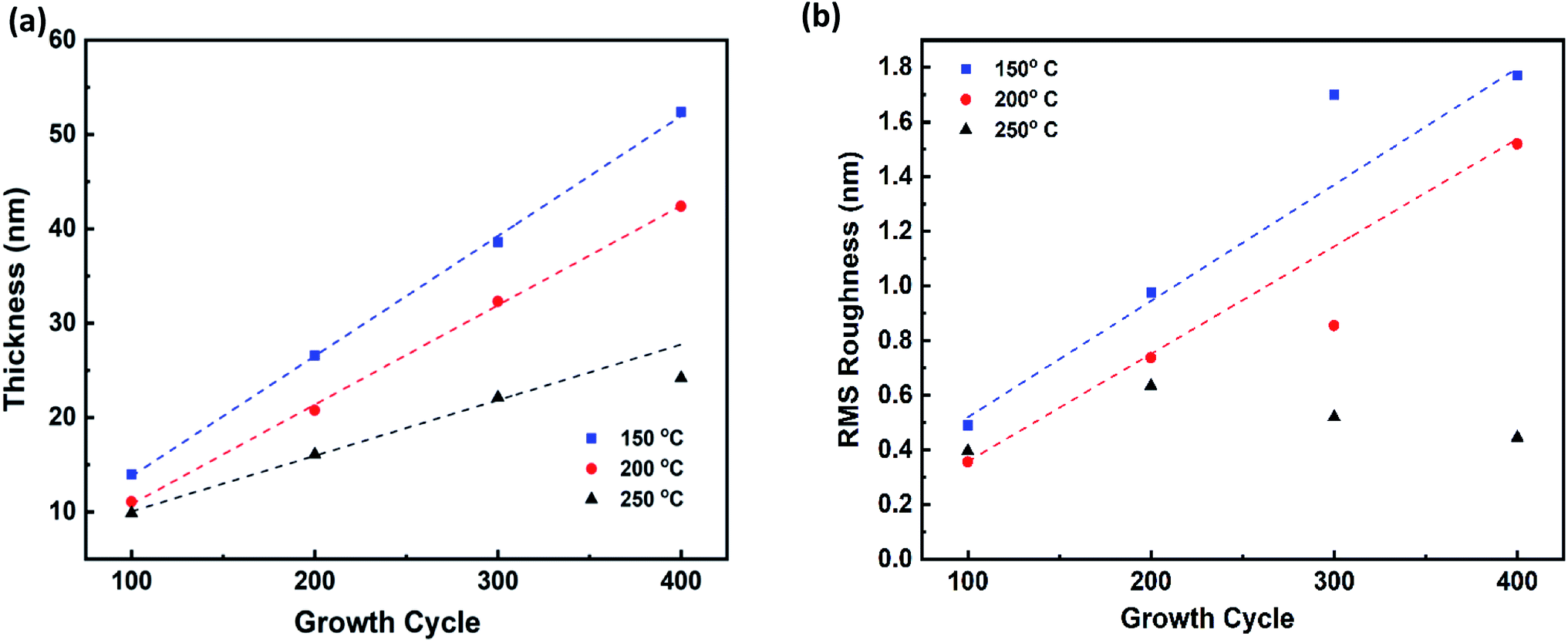 | ||
| Fig. 1 (a) Ellipsometer thickness of ZrO2 at different temperatures and number of cycles, (b) RMS roughness of ZrO2 from AFM measurements. | ||
As the film thickness and GPC have linear relations with the number of cycles and temperatures, the deposition rate is highly tunable in atomic scale. The hydrofluoric acid (HF) pretreatment of substrate induces a hydrophobic –H terminated surface on silicon.36 In our case, it is reasonable to believe an atomic layer starts growing from the very first cycle, and the large number of –OH nucleation sites on the silicon surface are created during the first water pulse of the ALD process. At all the deposition temperatures, ALD-ZrO2 followed a similar growth process i.e. layer-by-layer growth mode. At 250 °C, the absence of –OH sites are responsible for growth saturation which will be explained in later section.
For device applications, surface irregularity can influence adhesion and transport properties.37 The surface topology of the films was studied using atomic force microscopy (AFM). The RMS surface roughness curves in Fig. 1b, show linear trends at 150 and 200 °C. However, at first, the roughness rises slightly and then reduces with the number of cycles at 250 °C. This discrepancy in roughness is the result of static adatoms and the presence of residual Zr precursor ligands due to incomplete reaction at low temperatures. At 250 °C, the adatoms are more mobile and the Zr and O ions occupy the positions with the lowest free energy of the crystal.33 The surfaces are highly smooth as the roughness is less than 4% of the corresponding film thickness. The 3D surface topography of ZrO2 films at 150 °C is shown in Fig. 2 using an AFM scanned area of 500 × 500 nm2. Fig. 2a and b appear like tapered posts. The facets of the crystallites are more visible in Fig. 2c. The surface of Fig. 2d looks like hillocks with multiple valleys between them. These peaks are responsible for the highest surface roughness (1.77 nm) among all the samples, and a clear indication of precursor agglomeration at low temperature as the thermal energy during film growth was not enough to remove the zirconium precursor ligands completely.
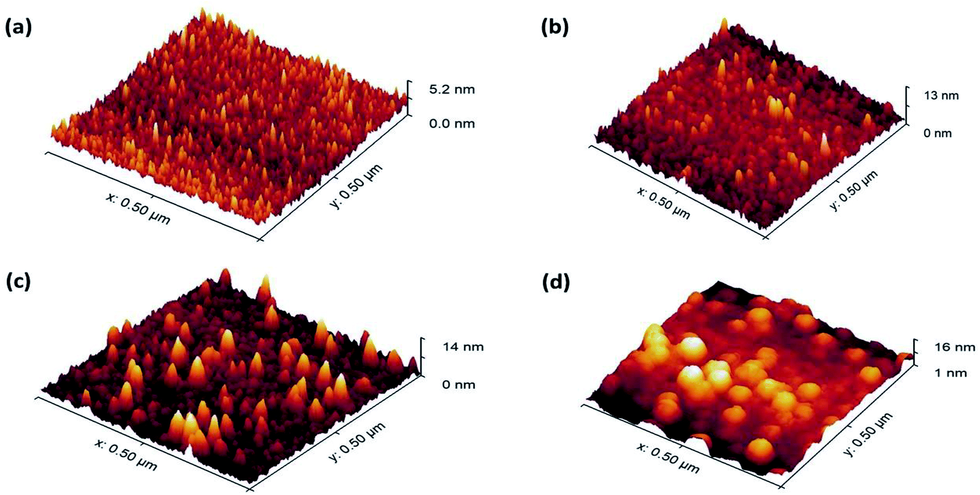 | ||
| Fig. 2 AFM surface images at 150 °C for growth cycles- (a) 100, (b) 200, (c) 300, (d) 400. | ||
The film thickness is a crucial factor in determining the crystal structure and phase of ZrO2.38 For 150 and 200 °C, the thickness of the films was deliberately kept high to study the role of thickness on crystallinity. The X-ray diffraction (XRD) measurements were performed in ALD-ZrO2 films of thickness 63, 46.4, and 22.3 nm for temperatures 150, 200, and 250 °C respectively. Fig. 3a shows the XRD spectra at various temperatures. At a low temperature (150 °C), the structure is amorphous as no noticeable peak is found in the XRD pattern. As the temperature increases, a sharp peak starts appearing in the angular position (2θ) of 33°. The intensity of the peak increases at higher temperatures. At 200 °C, a mixture of amorphous and crystalline states is present in the thin film. Nonetheless, a sharp peak at 250 °C in XRD pattern reveals the crystalline state of the deposited ZrO2. The peaks of XRD patterns can be indexed as (200) plane with cubic phase structure. Along with deposition, the crystallinity of ZrO2 is highly tunable from amorphous to crystalline phase with temperature alteration. Instead of the film thickness, the temperature is the crucial factor for crystallinity of ALD-ZrO2. The temperature influences the surface mobility of adatoms, reaction mechanism, and the number of nucleation sites. High temperatures promote the dehydroxylation, desorption, surface adatoms mobility and ordering of the structures with minimum surface energy which in turn reduce surface roughness. These phenomena lead to the crystalline structure of solids. With specific temperature provided, less surface roughness indicates more crystalline structure. Fig. S2 in the ESI† shows the variations of 2D surface topology with temperatures. The energy-dispersive spectra (EDS) confirms the presence of Zr, O, Si, and reveals no chemical contamination on the films (see ESI Fig. S3†).
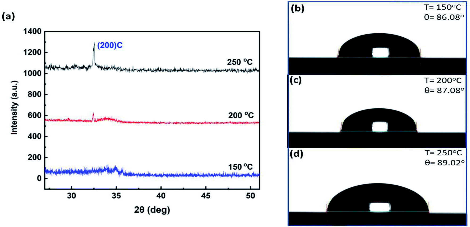 | ||
| Fig. 3 (a) XRD patterns of ZrO2 at different temperatures. Measured contact angles on ZrO2 for 400 cycles at: (b) 150 °C, (c) 200 °C, (d) 250 °C. | ||
A hydrophilic surface is expected to print an ink using an inkjet printer. To determine the hydrophilicity of our samples, we performed contact angle tests using water droplets as shown in Fig. 3b–d. As the contact angles are less than 90°, the surfaces are hydrophilic in general. As the temperature increased, the films showed more hydrophobic characteristics. Therefore, selection of proper deposition technique for ZrO2 is critical because hydrophobic ZrO2 by magnetron sputtering process was reported elsewhere.21 Our observations i.e. increase of contact angle with temperature, are quite opposite to the study of ref. 33 where a significant decrease of contact angles with temperature elevation was reported. Our claim can be refuted from the surface roughness, and dehydroxylation phenomena at higher temperatures. Water easily spreads on a hydroxylated surface. The –OH groups promote the hydrogen bonds with water, thus reducing the contact angle. Higher temperature leads to more dehydroxylation which reduces –OH nucleation sites on the deposition surface. Consequently, the deficiency of –OH sites increases the contact angles. Due to dehydroxylation at 250 °C, there is a scarcity of –OH bonds and the surface is nearly hydrophobic. This also strengthens the claim that the absence of –OH groups are responsible for the growth saturation in 300–400 cycles at 250 °C. The desorption effect is dependent on the deposition temperature as well as the time for which the processes were carried out. At 250 °C, the –OH nucleation sites were created during the water pulses of the ALD process. It is also true that a few –OH groups can stick to the growth surface at 250 °C. This high temperature increases the surface adatoms mobility and reorganizes the Zr–O structures based on the minimum surface energy. There should be less defect on the crystalline ALD-ZrO2 with reduced number of –OH sites available for nucleation. As the process at 250 °C was carried out for 300–400 cycles (almost 5 hours), the –OH groups get released (desorbed) from the surface. For longer process time, the absence of –OH nucleation sites are responsible for the growth saturation.
The roughness of a surface can be related to the contact angle by Wenzel's theory,39 cos(θA) = r![[thin space (1/6-em)]](https://www.rsc.org/images/entities/char_2009.gif) cos(θC), where θA is the apparent contact angle on a rough surface, θC is the contact angle on a smooth surface, r is the roughness factor which is the ratio of the real surface area to the projected surface area. According to Wenzel's relation, surface roughness makes the hydrophilic surface more hydrophilic, and the hydrophobic surface more hydrophobic. The roughness, real and projected surface area, and roughness factors are extracted from AFM measurements as shown in Table 1. As roughness factors are less than 1.5, Wenzel's relation is reasonable to apply in our case.40 As our samples are hydrophilic, roughness makes them more hydrophilic following Wenzel's statement. For 400 cycles, the roughness increases with temperature lowering, which enhances the real surface area and surface energy. Therefore, the surface turns more hydrophilic. Table 1 summarizes the relation between temperature, roughness, roughness factor, and contact angles.
cos(θC), where θA is the apparent contact angle on a rough surface, θC is the contact angle on a smooth surface, r is the roughness factor which is the ratio of the real surface area to the projected surface area. According to Wenzel's relation, surface roughness makes the hydrophilic surface more hydrophilic, and the hydrophobic surface more hydrophobic. The roughness, real and projected surface area, and roughness factors are extracted from AFM measurements as shown in Table 1. As roughness factors are less than 1.5, Wenzel's relation is reasonable to apply in our case.40 As our samples are hydrophilic, roughness makes them more hydrophilic following Wenzel's statement. For 400 cycles, the roughness increases with temperature lowering, which enhances the real surface area and surface energy. Therefore, the surface turns more hydrophilic. Table 1 summarizes the relation between temperature, roughness, roughness factor, and contact angles.
| Temperature (°C) | Roughness, Rq (nm) | Real surface area (nm2) | Projected surface area (nm2) | Roughness factor, r | θA (deg) | θC (deg) |
|---|---|---|---|---|---|---|
| 250 | 0.446 | 252012 |
250000 |
1.008 | 89.02 | 89.03 |
| 200 | 1.52 | 255146 |
250000 |
1.020 | 87.08 | 87.13 |
| 150 | 1.77 | 256834 |
250000 |
1.027 | 86.63 | 86.72 |
The dielectric properties of ZrO2 are studied by capacitance–voltage and parallel conductance–voltage characteristics at 100 kHz. The ALD-ZrO2 films were deposited on n-type Si wafers with the resistivity of 0.01–0.02 Ω cm. To evaluate the influence of the temperature on dielectric constant and interface traps, the oxide thicknesses were kept nearly identical such as 23.14, 21.17, and 22.3 nm for temperatures of 150, 200, and 250 °C respectively. The normalized C–V curves shown in Fig. 4a were obtained using a mercury probe. The capacitor area was 7.4 × 10⁻⁴ cm2. The C–V curves have distinguishable accumulation, depletion, and inversion regions. Dielectric constants (k) estimated from the electrical measurements are 7.5 (150 °C), 10.85 (200 °C), and 11 (250 °C) respectively. Due to crystallinity at higher temperatures, the dielectric constants improved about 1.46 times. Our observation of k value is lower, but consistent with the expected value of k for ZrO2 i.e. 10–25.41 For the device structures, the k-values were consistent with our reported dielectric constants. Ellipsometry is very sensitive to interfacial oxide, and we did not observe any signature of SiOX growth in our ellipsometry data. All our mean-square-error (MSE) values were less than 5. The breakdown field of the ALD-ZrO2 was ∼1 MV cm−1. We also examined the hysteresis behavior of the ALD-ZrO2 dielectric in Fig. S4 (see ESI†). The CV curves show a small hysteresis. Low hysteresis means there exists a good quality of ALD-ZrO2 dielectric/Si semiconductor interface. This low hysteresis is either due to the charge trapping in the ZrO2 or defect in the channel layer. Interestingly, the optical band gap calculated from the ellipsometer was fixed approximately at 4.82 eV for all our samples irrespective of the deposition temperatures, number of cycles, and crystal structure.
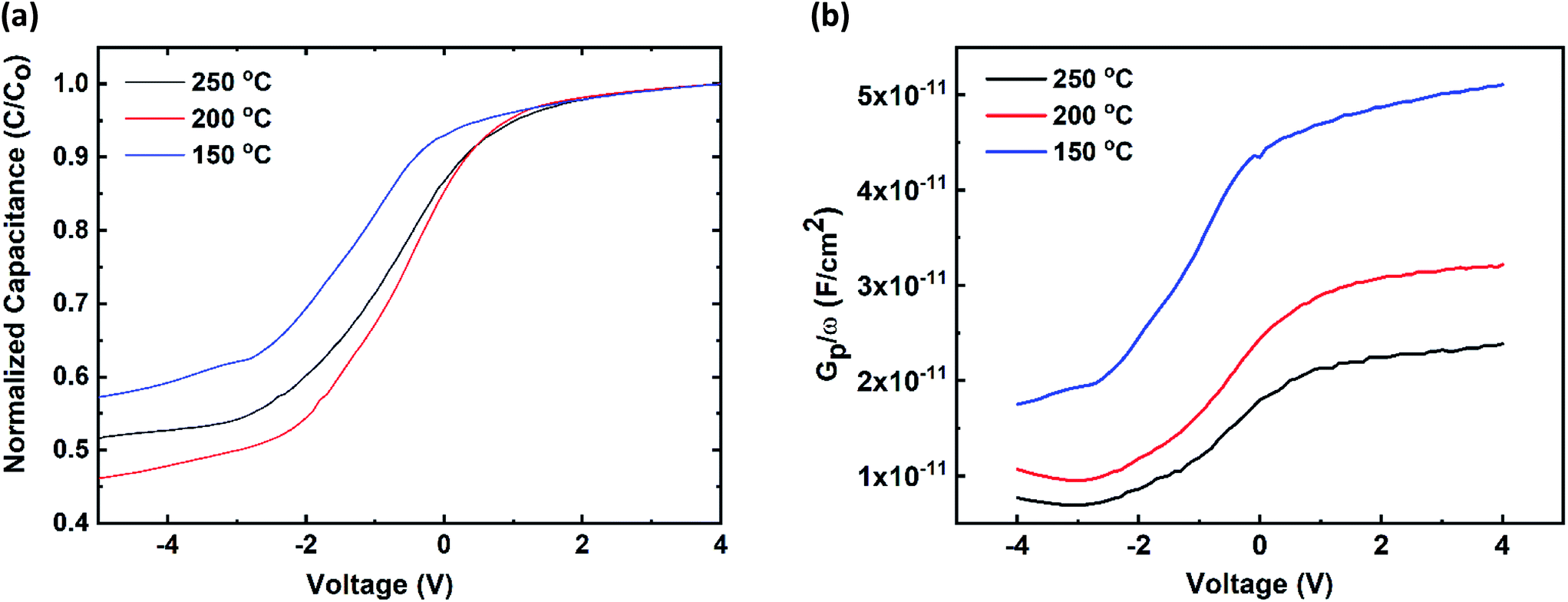 | ||
| Fig. 4 (a) Capacitance–voltage behaviors of Hg/ZrO2/Si-n (100) MOS capacitor, (b) Gp/ω curves at different voltages. | ||
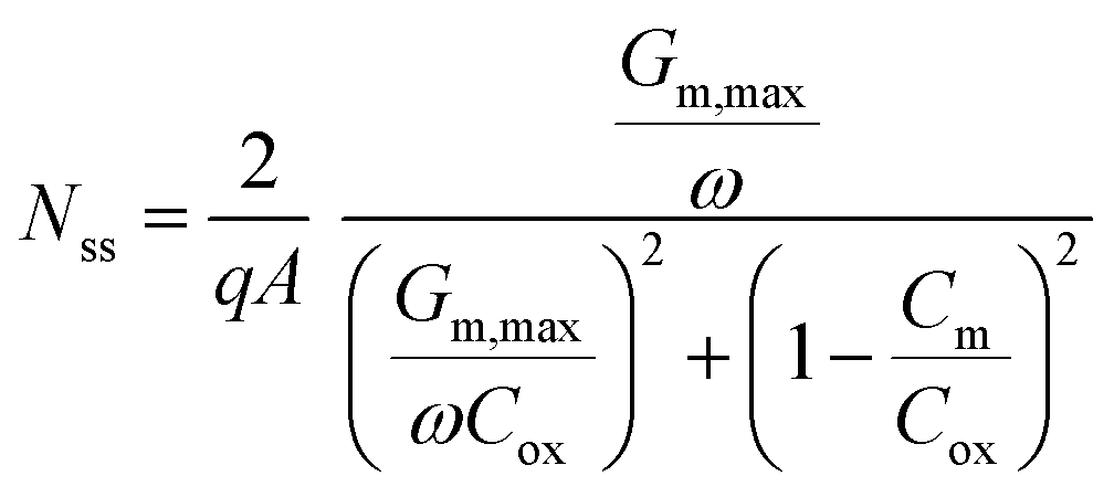
The conductance–voltage (Gp/ω−V) characteristics of MOS capacitors are shown in Fig. 4b. Conductance curves can be utilized to calculate the interface state density using the Hill-Coleman method as following:42
 | (4) |
2.3 Device fabrication
The details of graphene ink preparation, optical absorption spectrum, and Raman spectra are discussed in the ESI (Fig. S5†). The reliability of a gate dielectric depends on its ability to modulate the drain current and provide low gate leakage. Fig. 5a and b show the schematic and microscopic image of the bottom gate coplanar transistor structure with ALD-ZrO2 dielectric and inkjet printed graphene. The heavily doped n-type Si (100) wafer was used as the back-gate as well as the substrate. A ZrO2 dielectric layer of 46.4 nm thick was deposited at 200 °C. The source (S) and drain (D) electrodes were printed using silver nanoparticle ink (Novacentrix, Metalon® JS-B40G) followed by a thermal curing at 150 °C for 30 min. The printed silver developed a well-defined pattern on ZrO2 which was confirmed from the microscopic and SEM images. The silver adhered to the ZrO2 surface quite well as depicted in Fig. 5b. The width of the source and drain electrodes was 258.33 μm and the channel length was 113.33 μm. Multiple printing passes (12 times) of the graphene ink were performed to create a percolation cluster between source and drain terminals. For 12 printing passes, the average thickness of the printed graphene layers was approximately 53 nm. This satisfies the percolation threshold of printed graphene thickness of 25 nm for back-gated device.11 The graphene ink was prepared using terpineol and cyclohexanone solvents which are polar solvents. Using polar solvents, it is difficult to print a regular pattern on a hydrophobic surface. In a hydrophobic surface, they either form small droplets in the defined region, or the pattern collapses during curing. Despite the nearly hydrophobic behavior of the surfaces, we printed and cured graphene on the ZrO2 surface successfully. Fig. 5c shows the SEM image of the graphene percolating network. The projected area has good coverage with crumpling graphene flakes.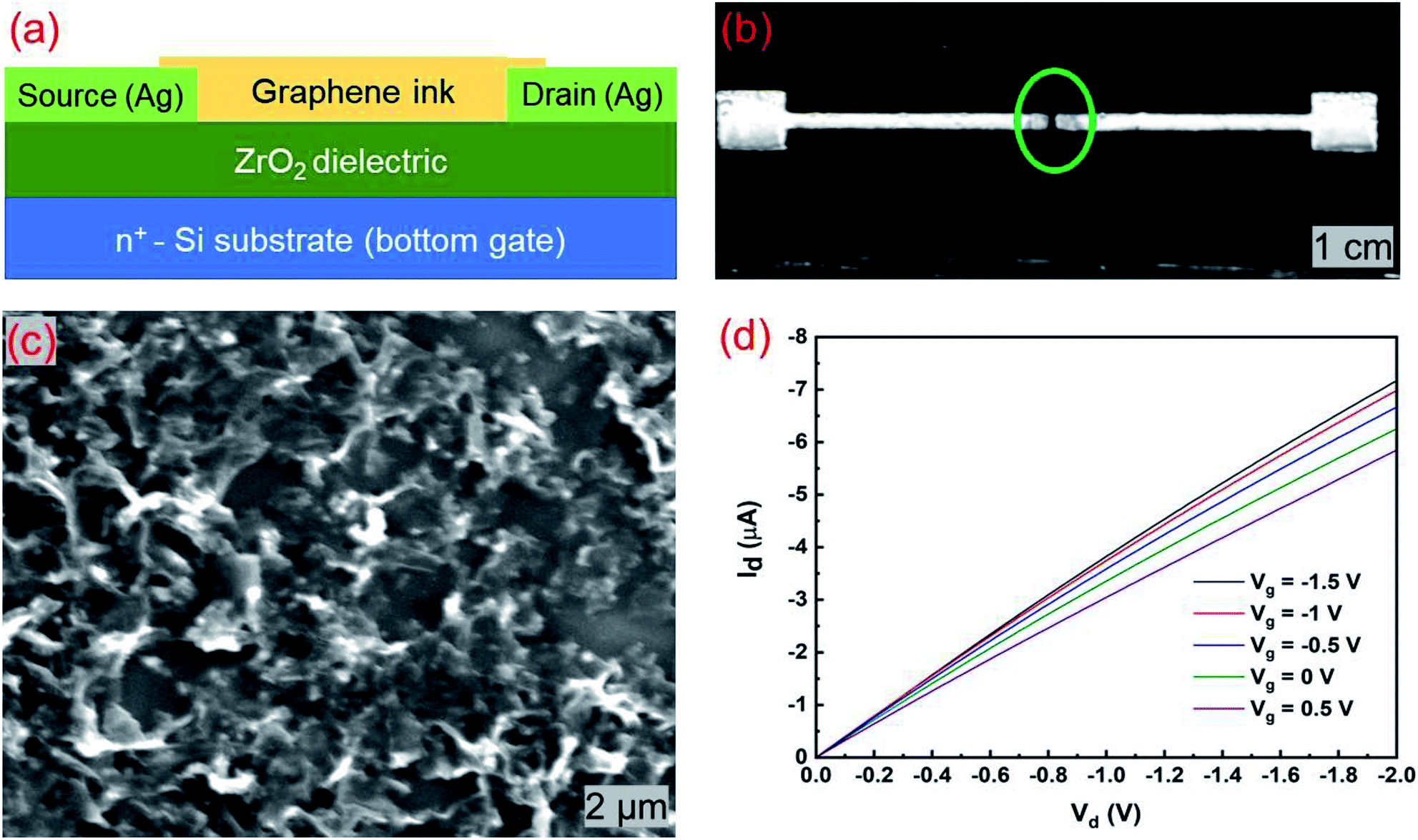 | ||
| Fig. 5 (a) Schematic of bottom-gate coplanar transistor, (b) microscopic image of printed graphene transistor, (c) SEM image of printed graphene, and (d) output characteristics of an inkjet-printed graphene transistor. | ||
Fig. 5d depicts the output (Id versus Vd) characteristics of the printed graphene transistor for several values of Vg. The gate voltage was changed from 0.5 to −1.5 V with a decrement of −0.5 V. The drain voltage also varied from 0 to −2 V for each value of Vg. The drain characteristics are linear. The trace of Id–Vd goes higher as the gate bias changes from positive to more negative. As Id increases with negative Vg, the transistor is of p-type. At Vd = −2 V, the drain current changes from −5.85 to −7.17 μA for a Vg variation of 2 V. This implies that the field-effect behavior due to the application of voltage on a thin ZrO2 layer is distinguishable from the output characteristics.
Transfer characteristics of printed graphene transistor is shown in Fig. S6 (see ESI†). Transfer characteristics were measured at the drain bias of −1, −1.5, and −2 V respectively. The gate–source leakage current (Isg) was very small (less than 20 nA). The drain current Id increases as the gate voltage goes from positive to negative. The charge neutrality (Dirac) point was outside of our measurement range. The unintentional doping may obscure the Dirac point in our measurement range. However, the gate modulation is well pronounced in the transfer characteristics at different drain biases. At Vd = −2 V, a current ON/OFF ratio of 1.46 is obtained from Fig. S6 in the ESI.† It is well-known that graphene does not have a band gap (zero band gap) and its transistor never turns off. So, it is unlikely to get a perfect off state and ON/OFF switching behavior from a graphene transistor. Small ON/OFF ratio and non-saturation are problems with all inkjet printed graphene transistors, due to the absence of bandgap in graphene. The effective mobility μ can be derived from the slope of the transfer characteristics using μ = (L × gm/W × Cox × Vd), where L (113.33 μm) and W (258.33 μm) are channel length and width, Cox is the gate capacitance (≈200 nF cm−2), and gm = dId/dVg is the transconductance (0.887 μS). The estimated device mobility is ≈1 cm2 V−1 s−1. For our graphene transistor, the current ON/OFF ratio and mobility is lower than the printed graphene transistor reported in ref. 11 but higher than the one reported in ref. 10. However, our results are still comparable to other inkjet printed graphene transistors.46 Therefore, the ALD grown thin oxide layers are suitable for low-voltage inkjet printed transistors.
3 Conclusion
A comprehensive study on growth kinetics and dielectric properties of the ALD-ZrO2 is conducted from TDMAZr precursor. Low-temperature growth of ZrO2 was achieved along with low roughness and high dielectric constant for different growth conditions. Linear relations of thickness and roughness were observed with growth cycles at different temperatures. The ALD temperature window for Zr(NMe2)4 precursor was determined from the growth saturation for 400 cycles at 250 °C. The crystallinity, the cubic phase, and the orientation in the (200) direction were observed at higher temperatures from the XRD patterns. The interface traps are due the defects in the ZrO2 films. In general, all our oxide surfaces were hydrophilic as the contact angles were less than 90°. The trend of contact angle change with temperature change is contrary to the previous report, and therefore opens a new venue for research in this direction. Graphene thin films of given patterns were deposited through inkjet printing on ZrO2 successfully. No significant differences of inkjet printed graphene on ZrO2 were noticed from Raman spectra. Finally, the printing of graphene transistors was realized using the bottom-gate coplanar structure with ZrO2 gate dielectric. A printed graphene transistor with a current on–off ratio of 1.46 at Vd = −2 V was achieved.Conflicts of interest
The authors declare no conflict of interest.Acknowledgements
This work was supported by Northrop Grumman Grant no. 2206730 and the National Science Foundation under MRI Grant No. 1625778. This work was also supported by the MSEC PhD program and Thesis Support Fellowship at Texas State University, San Marcos. We thank Dr Ravi Droopad, Dr Casey Smith, and Dr Dmitry Lyashenko for provided training and useful discussions.References
- M. Singh, H. M. Haverinen, P. Dhagat and G. E. Jabbour, Adv. Mater., 2010, 22, 673–685 CrossRef CAS PubMed.
- J. Chang, X. Zhang, T. Ge and J. Zhou, Org. Electron., 2014, 15, 701–710 CrossRef CAS.
- S. Chung, S. O. Kim, S. K. Kwon, C. Lee and Y. Hong, IEEE Electron Device Lett., 2011, 32, 1134–1136 CAS.
- P. M. Grubb, H. Subbaraman, S. Park, D. Akinwande and R. T. Chen, Sci. Rep., 2017, 7, 1202 CrossRef PubMed.
- B. Huber, P. Popp, M. Kaiser, A. Ruediger and C. Schindler, Appl. Phys. Lett., 2017, 110, 143503 CrossRef.
- T. M. Eggenhuisen, Y. Galagan, a. F. K. V. Biezemans, T. M. W. L. Slaats, W. P. Voorthuijzen, S. Kommeren, S. Shanmugam, J. P. Teunissen, A. Hadipour, W. J. H. Verhees, S. C. Veenstra, M. J. J. Coenen, J. Gilot, R. Andriessen and W. a. Groen, J. Mater. Chem. A, 2015, 3, 7255–7262 RSC.
- L. Zhou, L. Yang, M. Yu, Y. Jiang, C. F. Liu, W. Y. Lai and W. Huang, ACS Appl. Mater. Interfaces, 2017, 9, 40533–40540 CrossRef CAS PubMed.
- A. Moya, E. Sowade, F. J. del Campo, K. Y. Mitra, E. Ramon, R. Villa, R. R. Baumann and G. Gabriel, Org. Electron., 2016, 39, 168–176 CrossRef CAS.
- D. Soltman and V. Subramanian, Langmuir, 2008, 24, 2224–2231 CrossRef CAS PubMed.
- J. Li, F. Ye, S. Vaziri, M. Muhammed, M. C. Lemme and M. Östling, Adv. Mater., 2013, 25, 3985–3992 CrossRef CAS PubMed.
- F. Torrisi, T. Hasan, W. Wu, Z. Sun, A. Lombardo, T. S. Kulmala, G. W. Hsieh, S. Jung, F. Bonaccorso, P. J. Paul, D. Chu and A. C. Ferrari, ACS Nano, 2012, 6, 2992–3006 CrossRef CAS PubMed.
- W. Xu, H. Li, J. Bin Xu and L. Wang, ACS Appl. Mater. Interfaces, 2018, 10, 25878–25901 CrossRef CAS PubMed.
- M. A. Dominguez, O. Obregon and J. A. Luna-Lopez, J. Alloys Compd., 2016, 688, 893–896 CrossRef CAS.
- J. Leppäniemi, K. Eiroma, H. Majumdar and A. Alastalo, ACS Appl. Mater. Interfaces, 2017, 9, 8774–8782 CrossRef PubMed.
- J. Sheng, H. J. Jeong, K. L. Han, T. H. Hong and J. S. Park, J. Inf. Disp., 2017, 39, 1 Search PubMed.
- R. Zazpe, M. Knaut, H. Sopha, L. Hromadko, M. Albert, J. Prikryl, V. Gärtnerová, J. W. Bartha and J. M. Macak, Langmuir, 2016, 32, 10551–10558 CrossRef CAS PubMed.
- X. Meng, Y. Zhong, Y. Sun, M. N. Banis, R. Li and X. Sun, Carbon, 2011, 49, 1133–1144 CrossRef CAS.
- P. D. Ye, G. D. Wilk, J. Kwo, B. Yang, H. J. L. Gossmann, M. Frei, S. N. G. Chu, J. P. Mannaerts, M. Sergent, M. Hong, K. K. Ng and J. Bude, IEEE Electron Device Lett., 2003, 24, 209–211 CAS.
- Y. Q. Yang, Y. Duan, P. Chen, F. B. Sun, Y. H. Duan, X. Wang and D. Yang, J. Phys. Chem. C, 2013, 117, 20308–20312 CrossRef CAS.
- D. W. Park, S. Mikael, T. H. Chang, S. Gong and Z. Ma, Appl. Phys. Lett., 2015, 106, 102106 CrossRef.
- U. S. Patel, K. H. Patel, K. V. Chauhan, A. K. Chawla and S. K. Rawal, Proc. Technol., 2016, 23, 336–343 CrossRef.
- B. Kim, S. Jang, P. L. Prabhumirashi, M. L. Geier, M. C. Hersam and A. Dodabalapur, Appl. Phys. Lett., 2013, 103, 082119 CrossRef.
- Y. M. Park, A. Desai, A. Salleo and L. Jimison, Chem. Mater., 2013, 25, 2571–2579 CrossRef CAS.
- D. J. Burleson, J. T. Roberts, W. L. Gladfelter, S. A. Campbelland and R. C. Smith, Chem. Mater., 2002, 14, 1269–1276 CrossRef CAS.
- A. O. Dikovska, G. Atanasova, G. Avdeev and V. Strijkova, J. Phys.: Conf. Ser., 2016, 012024 CrossRef.
- M. F. Al-Kuhaili and S. M. a. Durrani, J. Alloys Compd., 2011, 509, 9536–9541 CrossRef CAS.
- D. M. Hausmann, E. Kim, J. Becker and R. G. Gordon, Chem. Mater., 2002, 14, 4350–4358 CrossRef CAS.
- Dupont Kapton data sheet (http://www.dupont.com/content/dam/dupont/products-and-services/membranes-and-films/polyimde-films/documents/DEC-Kapton-summary-of-properties.pdf).
- D. Y. Kim, S. Lee, Z.-H. Lin, K. H. Choi, S. G. Doo, H. Chang, J.-Y. Leem, Z. L. Wang and S.-O. Kim, Nano Energy, 2014, 9, 101–111 CrossRef CAS.
- J. Liu, X. Meng, Y. Hu, D. Geng, M. N. Banis, M. Cai, R. Li and X. Sun, Carbon, 2013, 52, 74–82 CrossRef CAS.
- J. Liu, X. Meng, M. N. Banis, M. Cai, R. Li and X. Sun, J. Phys. Chem. C, 2012, 116, 14656–14664 CrossRef CAS.
- Z. Chen, H. Wang, P. Xiong, P. Chen, H. Li, Y. Liu and Y. Duan, J. Phys. Chem. C, 2017, 121, 4714–4719 CrossRef CAS.
- Y. Duan, F. Sun, Y. Yang, P. Chen, D. Yang, Y. Duan and X. Wang, ACS Appl. Mater. Interfaces, 2014, 6, 3799–3804 CrossRef CAS PubMed.
- Y. C. Byun, J. G. Lee, X. Meng, J. S. Lee, A. T. Lucero, S. J. Kim, C. D. Young, M. J. Kim and J. Kim, Appl. Phys. Lett., 2017, 111, 082905 CrossRef.
- M. Cassir, F. Goubin, C. Bernay, P. Vernoux and D. Lincot, Appl. Surf. Sci., 2002, 193, 120–128 CrossRef CAS.
- J. Damlencourt, O. Renault, F. Martin, M. Semeria, T. Billon and F. Bedu, Appl. Phys. Lett., 2005, 86, 141913 CrossRef.
- M. Li, T. Marszalek, K. Müllen and W. Pisula, ACS Appl. Mater. Interfaces, 2016, 8, 16200–16206 CrossRef CAS PubMed.
- S. Sayan, N. V. Nguyen, J. Ehrstein, T. Emge, E. Garfunkel, M. Croft, X. Zhao, D. Vanderbilt, I. Levin and E. Gusev, et al., Appl. Phys. Lett., 2005, 86, 152902 CrossRef.
- R. N. Wenzel, Ind. Eng. Chem., 1936, 28, 988–994 CrossRef CAS.
- Y. Tamai and K. Aratani, J. Phys. Chem., 1972, 76, 3267–3271 CrossRef CAS.
- D. Panda and T.-Y. Tseng, Thin Solid Films, 2013, 531, 1–20 CrossRef CAS.
- W. Hill and C. Coleman, Solid-State Electron., 1980, 23, 987–993 CrossRef CAS.
- N. Chowdhury, R. Garg and D. Misra, Appl. Phys. Lett., 2004, 85, 3289–3291 CrossRef CAS.
- A. Tamm, J. Kozlova, T. Arroval, L. Aarik, P. Ritslaid, H. García, H. Castán, S. Dueñas, K. Kukli and J. Aarik, Chem. Vap. Deposition, 2015, 21, 181–187 CrossRef CAS.
- A. Zoolfakar, Mater. Res. Innovations, 2009, 13, 161–164 CrossRef CAS.
- C. Petridis, Y.-H. Lin, K. Savva, G. Eda, E. Kymakis, T. Anthopoulos and E. Stratakis, Appl. Phys. Lett., 2013, 102, 093115 CrossRef.
Footnote |
| † Electronic supplementary information (ESI) available: ALD process, 2D AFM and SEM images of ZrO2 of thickness 38.58, 32.51,22.2 and 46.4 nm prepared at 150, 200, and 250 °C; EDS spectra at 150, 200, and 250 °C. Hysteresis in the ALD-ZrO2 dielectric; graphene ink preparation, UV-vis, and Raman characterization; transfer curves of printed graphene transistor. See DOI: 10.1039/c8ra08470j |
| This journal is © The Royal Society of Chemistry 2019 |