
 Open Access Article
 This Open Access Article is licensed under a Creative Commons Attribution-Non Commercial 3.0 Unported Licence
Film formation from plasma-enabled surface-catalyzed dehalogenative coupling of a small organic molecule†
Hugo Hartl a,
Yanru Guoab,
Ken Ostrikovac,
Yubin Xiand,
Jie Zhengb,
Xingguo Lib,
Kathryn E. Fairfull-Smitha and
Jennifer MacLeod*a
a,
Yanru Guoab,
Ken Ostrikovac,
Yubin Xiand,
Jie Zhengb,
Xingguo Lib,
Kathryn E. Fairfull-Smitha and
Jennifer MacLeod*a
aSchool of Chemistry, Physics and Mechanical Engineering, Queensland University of Technology (QUT), 2 George Street, Brisbane, QLD, Australia 4000. E-mail: jennifer.macleod@qut.edu.au
bBeijing National Laboratory for Molecular Sciences (BNLMS), College of Chemistry and Molecular Engineering, Peking University, Beijing 100871, P. R. China
cCSIRO-QUT Joint Sustainable Processes and Devices Laboratory, P. O. Box 218, Lindfield, NSW 2070, Australia
dState Key Laboratory of Advanced Electromagnetic Engineering and Technology, School of Electrical and Electronic Engineering, Huazhong University of Science and Technology, Wuhan, Hubei 430074, People's Republic of China
First published on 21st January 2019
Abstract
This work demonstrates a new pathway to the direct on-surface fabrication of surface coatings by showing that application of a plasma can lead to dehalogenative coupling of small aromatic molecules at a catalytic surface. Specifically, we show that a room temperature, atmospheric pressure plasma can be used to fabricate a coating through a surface-confined dehalogenation reaction. Plasma treatments were performed using a dielectric barrier discharge (DBD) technique under pure nitrogen with a variety of power levels and durations. Samples were analysed by optical and helium ion microscopy (HIM), X-ray photoelectron spectroscopy (XPS), optical profilometry, and contact angle measurement. By varying the plasma parameters we could control the chemistry, morphology and roughness of the film. Surface wettability also varied with the plasma parameters, with high-dose plasmas leading to a hydrophobic surface with water contact angles up to 130°.
Introduction
In recent years, on-surface coupling reactions have emerged as a powerful approach to synthesize novel materials.1–4 The general scheme is to introduce small molecules to a surface, and to subsequently react them so that they covalently couple into an extended film. The work has largely been focused on the fabrication of low-dimensional materials, for example the growth of graphene by chemical vapour deposition or molecular beam epitaxy,5,6 or the synthesis of novel 1D and 2D nanomaterials with controlled structure and composition.7,8 Typically, the molecules are deposited from the gas phase onto the substrate and are then thermally activated with the surface acting as a catalyst for the coupling reaction. The attractive interaction between the deposited molecules and the substrate means that as the polymer film grows, the catalyst is passivated, and film growth is therefore limited to monolayer (or few-layer) films.While these Angstrom-thick films are desirable for many applications, there also exists a range of situations in which a thicker film is advantageous, such as for applications where surface morphologies can be used to modify light scattering, wettability, tribological properties and cell response,9–12 and where direct, in situ synthesis on a surface could be useful for film fabrication. Here, we demonstrate a synthesis approach that produces micron-thick films with tailored morphologies through a catalyzed reaction of small molecules at a metal surface. Surface-catalyzed coupling often requires high temperatures, and molecular desorption cam pose a problem for creating high-coverage or thick films. We circumvent these challenges by using a liquid-phase precursor that allows for dynamic exchange of the molecules in contact with the surface catalyst, and by activating the room-temperature reaction through plasma treatment.
For the last few decades the effects of plasma on catalysis has been an active area of investigation.13,14 Atmospheric-pressure plasma treatment was shown to facilitate low-temperature reactions by increasing the yield of the desired product and minimizing unwanted by-products.15 Employing atmospheric plasmas with a catalyst present has the advantage of reducing the operating temperature, which offers significant energy savings.16 Alongside this development of plasma catalysis, the understanding and use of plasma in liquids have been expanding.17 The interaction of plasmas with water has been the subject of many investigations,18 however the ionization mechanism of liquids with larger molecular structures are not yet fully understood.19,20 The environment produced when a plasma interacts with a liquid is complex: discharges in contact with liquids produce radicals, shock waves in the liquid, and UV radiation.21,22 Different processes occur in the bulk plasma, in the liquid, and at the interface of the plasma–liquid. In the bulk plasma, ions will be driven into the liquid from the source, where they will create knock-on effects such as secondary electrons and decomposition of the liquid solutions.23 The components from the liquid solution can be sputtered into the bulk plasma.24 Together, these effects create a highly reactive environment.
In this work, we use plasma treatment of an organic liquid at a catalytic interface to produce a surface-bound solid film. We demonstrate that plasma treatment promotes a metal-catalyzed reaction to cleave C–X (carbon–halogen) bonds in the presence of a transition metal surface. C–X bonds have low dissociation energies, and can undergo catalytic cleaving via the well-known Ullmann reaction, where copper acts as a catalyst for C–X bond cleavage and subsequent aryl–aryl coupling.25 Ullmann-type coupling on metal surfaces usually occurs at elevated temperatures.26 In the present work, room-temperature atmospheric plasma treatment is used to induce C–X bond scission, with subsequent coupling of the reactive intermediates, in the presence of a transition-metal catalyst surface. We investigated the effect of both plasma power levels and dose times, and characterized the product through optical microscopy, helium ion microscopy (HIM), X-ray photoelectron spectroscopy (XPS), and optical profilometry. Functional properties were investigated through contact angle measurements. Together, the results indicate that plasma-assisted dehalogenative coupling is occurring, and that the morphology, chemistry and wettability of the film can be controlled through tuning the plasma parameters.
Materials and methods
We selected 1,2,4-trichlorobenzene (TCB, Fig. 1) as our monomer for this investigation, as the molecule is liquid at room temperature, allowing us to exploit plasma–liquid interactions and as well as providing immediate visible feedback on whether the reaction was progressing through the formation of a solid-phase product. | ||
| Fig. 1 Plasma catalytic experimental setup. | ||
All the plasma treatments were performed using a dielectric barrier discharge (DBD) technique at room temperature. Samples were placed on a quartz plate with a high-voltage AC generator (CTP-2000 K, Corana Laboratory). Nitrogen gas was applied as the working gas to minimize the oxidation of the surface, and because nitrogen-containing carbon films are good candidates for a number of applications, such as supercapacitor electrodes.27
Au and Ni were chosen as substrates due to their differing catalytic ability.28 Substrates were prepared by depositing 50 nm Au and Ni films onto 5 mm × 5 mm Si(100) wafers (Ted Pella, Inc.) using electron beam deposition. The metals were deposited at a rate of 2 Å s−1 onto room-temperature substrates. The Si was not stripped of oxide prior to deposition, so a typical native oxide layer should be present at the metal/Si interface.
For synthesis experiments, 1 μL of TCB was deposited on each stationary metal-coated substrate using an auto-pipette. The TCB fully wetted each substrate, creating a convex film with a maximum thickness of ∼0.5 mm (see ESI†). An uncoated Si wafer was used as a control sample. A schematic of the sample geometry used in these experiments is shown in Fig. 1.
Immediately after precursor deposition, each sample was treated with plasma, and the resulting film was subsequently characterized. For both sample sets, we used the same peak–peak generator output voltages (30 kV/50 kV/70 kV) measured by a PINTEK HVP-39pro high-voltage probe and Rigol oscilloscope. These high voltages were achieved by use of a 0–250 V input voltage regulator feeding the CTP-2000 K. The plasma characteristics, including waveform and power output, are consistent with those reported by others using the same equipment.29 The output power of the plasma should increase linearly with increasing voltage, as the output current and frequency were kept constant at ∼2 mA and ∼10 kHz. For the dielectric barrier (which is characterised by the dielectric constant and thickness), the operating frequency is adjusted for the optimum DBD generation. The output power of the CTP-2000 K generator may be estimated as 0.8× the input power.30 Therefore, the plasma produced at 30 kV/50 kV/70 kV output voltage would correspond to an estimated output power of approximately 48 W/80 W/112 W. A typical waveform is presented in the ESI.†
The substrate and plasma conditions for each sample are reported in Table 1. In our first set of samples, we tested the effect of increasing discharge voltage at constant time. In another set of experiments, we investigated the relationship between total plasma dose on the film composition and topography. For the constant-dose sample set, three time intervals were chosen such that the product of the output power and time was held approximately constant. The intent of the different sample sets was to elucidate whether the total dose on the film or the higher power levels, independent of time, are more important for determining film properties.
| Constant-time samples | |||
|---|---|---|---|
| Au (min) | Ni (min) | Si (min) | |
| 30 kV | 5 | 5 | 5 |
| 50 kV | 5 | 5 | — |
| 70 kV | 5 | 5 | — |
| Constant-dose samples | ||
|---|---|---|
| Au (min) | Ni (min) | |
| 30 kV | 3.5 | 3.5 |
| 50 kV | 2 | 2 |
| 70 kV | 1.5 | 1.5 |
We note that the different output voltages (and hence, power coupled to the plasma) may potentially produce reactive species in different ionization, excitation, and dissociation states.31–34 Therefore two identical doses, with the same total energy deposited, may generate different composition of reactive plasma species, which may in turn affect the plasma-assisted surface reactions. Some understanding of the species present in the plasma can be gained from optical emission spectroscopy (OES), which we used to identify the spectral features generated in the plasma. In Fig. 2 we present the OES intensities of emitted radiation measured as a function of input voltage in the wavelength range of 300–600 nm. Distinct peaks in the 300–500 nm region correspond to emissions of excited N2 species caused by many excitation and quenching processes. The emissions increase in intensity as the input voltage is increased, confirming that amounts of reactive nitrogen species (RNS) increase when increasing the voltage, however no new spectral lines were found throughout the range.
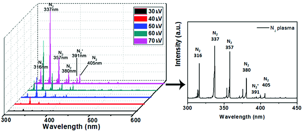 | ||
| Fig. 2 OES of N2 plasma in a DBD technique as a function of input voltage. | ||
Rotational and vibrational temperatures were simulated by peak fitting of the OES data in Specair (see Fig. A.8†). Temperatures of 300 K rotational and 2400 K vibrational were estimated for the 30 kV plasma. The 50 kV and 70 kV plasma were both estimated to have temperatures of 450 K rotational and 2450 K vibrational. This in combination with the increased number of reactive species seen as the plasma voltage increased are suggested as the cause of the increasing substrate temperatures that were witnessed (see Table A.3†).
Helium ion microscopy (HIM, Zeiss Orion Nanofab) and optical microscopy (Leica DM6000M) were used to investigate the morphology of the product on the surface. X-ray photoelectron spectroscopy (XPS, Kratos Axis Supra) using an Al Kα source (1486.87 eV) and with 225 W emission power was used to chemically characterize films. A step size of 0.1 eV for 60 s sweep time was used for region scans, and 1.0 eV for 120 s for wide scans. All measurements were performed at room temperature. XPS analysis was performed in CasaXPS Version 2.3.18.35 Laser confocal microscopy (Olympus LEXT OLS4100) was used to measure surface roughness. A contact angle setup (FTÅ200) was used to measure the contact angle of a water droplet dropped onto the surface of different films at a rate of 2 μL s−1.
Results
Optical microscopy
During plasma processing, we observed a liquid-to-solid transition of the TCB, consistent with the formation of higher molecular weight products. Optical microscopy revealed that the morphology of the resulting film depends on the plasma parameters and substrate type.The morphologies can be classified into three regimes, which occur sequentially with increasing plasma power:
(1) Patchy
(2) Spinodal
(3) Dewetted droplets.
At low plasma exposure, the films are very smooth, with irregular patches that appear to reveal the substrate. With increasing exposure, the films take on a complex morphology that comprises radially-concentric sunburst-type features coexisting with a spinodal-like phase. As the plasma processing progresses, we see small dewetted-style droplets forming within the spinodal regions and with increasing plasma exposure these dewetted droplets become the dominant features in the film. These phases are shown in the optical micrographs in Fig. 3 and 4.
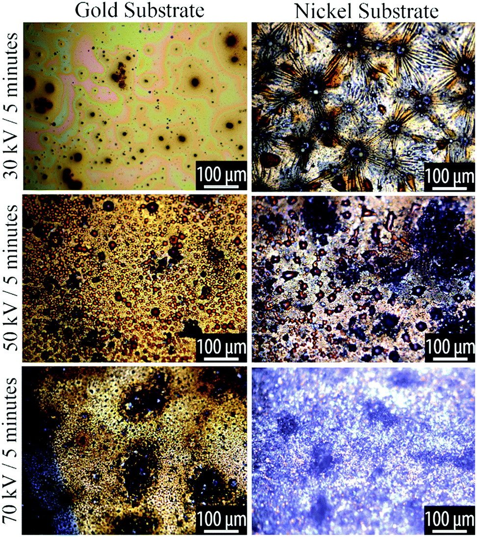 | ||
| Fig. 3 Optical microscopy of plasma reacted TCB on Au and Ni substrates, at varying powers for 5 minutes. Voltage and time parameters are specified along the vertical axis of the figure. | ||
 | ||
| Fig. 4 Optical microscopy of plasma reacted TCB on Au and Ni substrates, at varying powers and durations but constant total dose. Voltage and time parameters are specified along the vertical axis of the figure. | ||
Helium ion microscopy
HIM was used for imaging of surface morphology due to its compatibility with charge-compensation by use of a flood gun, which provides advantage over traditional SEM techniques for imaging nonconductive and poorly conducting materials.36 HIM shows the same features revealed by optical microscopy. Typical morphological features are shown in Fig. 5 and 6. | ||
| Fig. 5 HIM image of plasma reacted TCB on Au and Ni substrates, at varying powers for 5 minutes. Voltage and time parameters are specified along the vertical axis of the figure. | ||
 | ||
| Fig. 6 HIM image of plasma reacted TCB on Au and Ni substrates, at varying powers and durations but constant total dose. Voltage and time parameters are specified along the vertical axis of the figure. | ||
X-ray photoelectron spectroscopy
XPS was used to investigate the composition of the films. Table 2 and Fig. 7 summarize the elemental composition of the plasma-processed samples, based on quantification of the XPS survey scans. The tabulated TCB stoichiometry is included, for comparison, in Table 2. In all cases, samples with catalytic metal layers produced a decrease in the Cl![[thin space (1/6-em)]](https://www.rsc.org/images/entities/char_2009.gif) :C ratio, whereas the control sample exhibited a Cl:C ratio consistent with intact TCB (Fig. 8 and 9). Furthermore, the Cl:C ratio decreased with increasing plasma power, and was generally lower for samples with a Ni catalytic layer than Au under identical processing conditions. The highest degree of dehalogenation was observed in the Ni sample exposed to the 70 kV plasma for 5 minutes, which corresponds to our highest tested plasma dose. The processing conditions also affected the amount of oxygen and nitrogen present in the films. Higher plasma power levels correlated with an increased incorporation of both nitrogen and oxygen within the films. Results of testing with constant total dose showed that for a given substrate, the Cl:C ratio remained constant for all power levels (Table 3). The fraction of the total stoichiometry that was nitrogen also remained quite similar in the film.
:C ratio, whereas the control sample exhibited a Cl:C ratio consistent with intact TCB (Fig. 8 and 9). Furthermore, the Cl:C ratio decreased with increasing plasma power, and was generally lower for samples with a Ni catalytic layer than Au under identical processing conditions. The highest degree of dehalogenation was observed in the Ni sample exposed to the 70 kV plasma for 5 minutes, which corresponds to our highest tested plasma dose. The processing conditions also affected the amount of oxygen and nitrogen present in the films. Higher plasma power levels correlated with an increased incorporation of both nitrogen and oxygen within the films. Results of testing with constant total dose showed that for a given substrate, the Cl:C ratio remained constant for all power levels (Table 3). The fraction of the total stoichiometry that was nitrogen also remained quite similar in the film.
| Sample | O (%) | C (%) | N (%) | Si (%) | Au (%) | Cl (%) | Ni (%) | Cl:C |
|---|---|---|---|---|---|---|---|---|
| TCB | — | 66.6 | — | — | — | 33.3 | — | 0.50 |
| 30 kV Si | 7.0 ± 0.2 | 57.2 ± 0.4 | 6.7 ± 0.3 | — | — | 29.2 ± 0.3 | — | 0.51 ± 0.02 |
| 30 kV Au | 12.8 ± 0.3 | 61.5 ± 0.4 | 2.7 ± 0.3 | 8.2 ± 0.3 | — | 14.8 ± 0.3 | — | 0.24 ± 0.02 |
| 50 kV Au | 14.1 ± 0.3 | 59.4 ± 0.5 | 7.4 ± 0.3 | 1.5 ± 0.3 | — | 17.6 ± 0.2 | — | 0.30 ± 0.02 |
| 70 kV Au | 14.3 ± 0.3 | 60.0 ± 0.4 | 14.6 ± 0.3 | 2.2 ± 0.2 | — | 9.0 ± 0.2 | — | 0.15 ± 0.02 |
| 30 kV Ni | 13.1 ± 0.3 | 62.0 ± 0.4 | 10.3 ± 0.3 | 1.1 ± 0.2 | — | 12.6 ± 0.2 | 0.9 ± 0.1 | 0.20 ± 0.02 |
| 50 kV Ni | 8.8 ± 0.3 | 63.6 ± 0.5 | 6.3 ± 0.3 | 0.7 ± 0.2 | — | 20.3 ± 0.3 | 0.3 ± 0.1 | 0.32 ± 0.02 |
| 70 kV Ni | 8.8 ± 0.3 | 70.0 ± 0.4 | 12.7 ± 0.3 | 2.4 ± 0.2 | — | 5.8 ± 0.2 | 0.2 ± 0.1 | 0.08 ± 0.03 |
 | ||
| Fig. 7 Survey scans by XPS showing important spectral peaks for (a) Au substrate samples (b) Ni substrate samples. | ||
 | ||
| Fig. 8 The Cl:C ratio of all constant time plasma samples. The blue line shows the C:Cl ratio of the TCB precursor. | ||
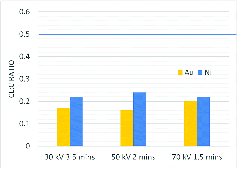 | ||
| Fig. 9 The Cl:C ratio of all constant total dose plasma samples. The blue line shows the C:Cl ratio of the TCB precursor. | ||
| Sample | O (%) | C (%) | N (%) | Si (%) | Au (%) | Cl (%) | Ni (%) | Cl:C |
|---|---|---|---|---|---|---|---|---|
| 30 kV 3.5 min Au | 18.1 ± 0.3 | 57.8 ± 0.4 | 11.5 ± 0.3 | 2.6 ± 0.3 | 0.3 ± 0.1 | 9.9 ± 0.2 | — | 0.17 ± 0.02 |
| 50 kV 2 min Au | 17.2 ± 0.2 | 55.6 ± 0.4 | 14.8 ± 0.3 | 3.2 ± 0.2 | — | 9.2 ± 0.2 | — | 0.16 ± 0.03 |
| 70 kV 1.5 min Au | 15.7 ± 0.3 | 58.1 ± 0.4 | 11.0 ± 0.4 | 3.1 ± 0.3 | 0.1 ± 0.1 | 12.1 ± 0.2 | — | 0.20 ± 0.02 |
| 30 kV 3.5 min Ni | 19.5 ± 0.3 | 55.5 ± 0.4 | 10.0 ± 0.3 | 1.2 ± 0.3 | — | 12.0 ± 0.2 | 1.9 ± 0.1 | 0.22 ± 0.03 |
| 50 kV 2 min Ni | 15.9 ± 0.3 | 58.5 ± 0.4 | 9.9 ± 0.3 | 1.2 ± 0.2 | — | 13.8 ± 0.2 | 0.7 ± 0.1 | 0.24 ± 0.02 |
| 70 kV 1.5 min Ni | 14.9 ± 0.3 | 59.1 ± 0.4 | 11.5 ± 0.3 | 1.2 ± 0.2 | — | 12.8 ± 0.2 | 0.6 ± 0.1 | 0.22 ± 0.02 |
Optical profilometry
Film roughness properties were determined using optical profilometry. Here, we focus on the parameters Sq (RMS or standard deviation of heights of the structures on the sample surface) and Sz (maximum height of film features, based on the sum of the largest peak height value and the largest pit depth value within the defined area), which were extracted from this analysis. Both parameters are compliant with ISO 25178 (international standard for analysis of 3D areal surface texture).Analysis of the RMS roughness results show that the constant-time films are roughest at 50 kV. Overall the RMS roughness is higher for all samples that were dosed for a constant time (5 minutes) as compared to the constant-dose samples (Table 4). The constant-dose samples show an increasing trend in RMS roughness with voltage.
| Sample | Au | Ni | ||
|---|---|---|---|---|
| Sq (μm) | Sz (μm) | Sq (μm) | Sz (μm) | |
| 30 kV 5 min | 0.23 ± 0.06 | 1.80 ± 0.37 | 1.73 ± 0.82 | 15.57 ± 5.04 |
| 50 kV 5 min | 2.53 ± 0.16 | 12.90 ± 0.60 | 2.55 ± 0.21 | 13.53 ± 1.15 |
| 70 kV 5 min | 1.15 ± 0.04 | 10.44 ± 2.64 | 1.65 ± 0.11 | 12.82 ± 1.66 |
| 30 kV 3.5 min | 0.09 ± 0.06 | 1.39 ± 0.74 | 0.06 ± 0.01 | 0.85 ± 0.11 |
| 50 kV 2 min | 0.82 ± 0.13 | 4.73 ± 0.41 | 1.00 ± 0.14 | 5.95 ± 0.91 |
| 70 kV 1.5 min | 1.00 ± 0.11 | 4.57 ± 0.45 | 1.25 ± 0.11 | 5.19 ± 0.49 |
The measured maximum heights reveal micron-scale features on all samples, with the constant-time samples uniformly showing higher values than the constant-dose samples (Table 4). As with the RMS roughness data, the constant-dose samples show a better-defined trend than the constant-time samples, with the maximum feature size exhibiting a well-defined maximum at 50 kV.
Contact angle measurements
The contact angle between a water droplet and the substrate is related to the wettability of a solid, with greater angles indicating lower wettability.37 Contact angle measurements were made after long-term exposure to ambient, with initial measurement at 90 days after film synthesis, and a subsequent measurement at 180 days (see ESI†). These second measurements revealed no change in the films, with wettability figures staying constant within uncertainty between the two time periods.Table 5 shows the contact angle data for samples where the plasma treatment time was held constant. As the plasma power increased from 30 to 70 kV, so did the contact angle, indicating that the films are increasingly hydrophobic as the plasma power is increased (varying from a contact angle of ∼70°/∼70° Au/Ni to a contact angle of ∼110°/∼130° Au/Ni).
| Sample | Au (°) | Ni (°) |
|---|---|---|
| 30 kV 5 min | 76.0 ± 6.7 | 71.0 ± 7.8 |
| 50 kV 5 min | 90.0 ± 0.6 | 89.7 ± 8.1 |
| 70 kV 5 min | 111.7 ± 13.7 | 134.7 ± 2.7 |
| 30 kV 3.5 min | 51.0 ± 4.6 | 56.3 ± 4.9 |
| 50 kV 2 min | 66.0 ± 2.5 | 58.3 ± 9.3 |
| 70 kV 1.5 min | 87.7 ± 1.3 | 58.7 ± 7.5 |
For the sample set where the total plasma dose was held constant (Table 5), the gold samples showed an increase in contact angle with an increase in plasma power, though at a much smaller rate than when time was kept constant. In the nickel samples all measurements are identical within uncertainty. Fig. 10 shows the captured contact angle images.
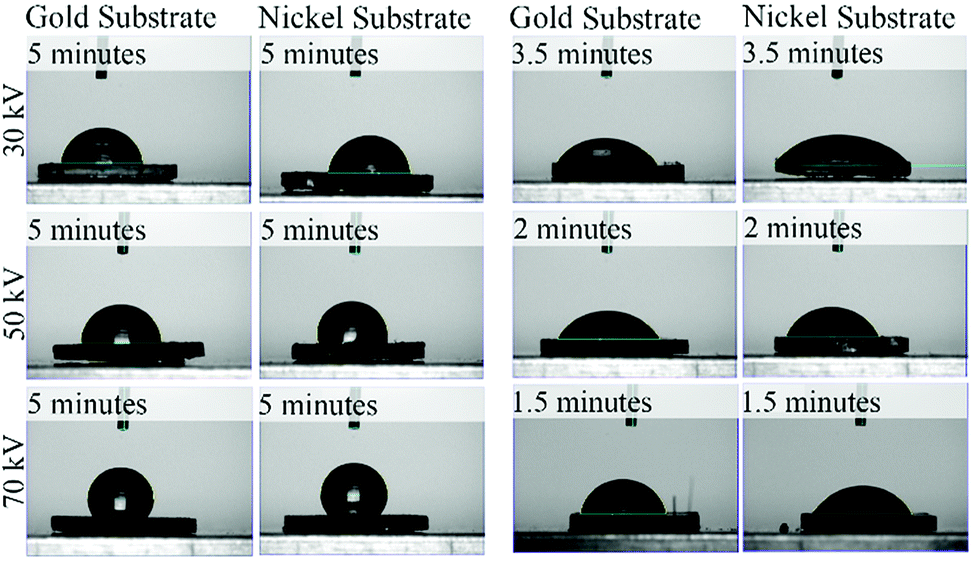 | ||
| Fig. 10 Contact angle images for all samples produced. | ||
Discussion
Chemical composition of the films
During the plasma treatment of the liquid-phase TCB on catalytic substrates, we were able to visibly discern the formation of a distinct solid product phase coexisting with the liquid-phase TCB. Following plasma interaction, it was evident that a solid thin film had formed on the substrate. This phase change is consistent with the formation of oligomers and/or polymers, which are insoluble in the TCB and precipitate out as a solid product.Our visual observations suggested that during plasma exposure, the monomer was split by the plasma into reactive fragments, which then crosslinked to form oligomeric/polymeric product that deposited on the substrate as a thin film.38 On metal surfaces, the solid product had a lower stoichiometric content of Cl than the intact molecule, which suggests that we are observing a plasma-assisted catalytic dehalogenation of TCB.
Not all experiments produced thick, film-like product; plasma voltages below 20 kV were not sufficient to cause the necessary reaction over 5 minutes (despite creating a plasma), and were not included in this analysis due to the lack of a solid product. Similarly, on the control (silicon) sample, only a thin and inhomogenous film was formed; since the XPS results show that Cl was not preferentially cleaved in this film, the formation of the solid product could be attributed to C–H bond breaking and subsequent molecular coupling.
Ullmann coupling on surfaces is generally conducted at elevated temperatures (around 80–110 °C at minimum), although photons and electrons have also been used to activate the reaction at room temperature.4,39,40 Under plasma treatment, gas ions, electrons, and radicals are all accelerated toward the surface, where they can transfer energy and cleave chemical bonds.41 Hence, under our experimental conditions, the excited species that are created during the plasma process are likely interacting with our halogenated molecule and catalyst substrate, causing the dehalogenation reaction to proceed at much lower temperatures than usual. Since both electrons40 and photons43 have previously been found to initiate dehalogenation in the presence of a suitable Ullmann catalyst, we can assume that one of these factors may play a dominant role here. However, we also cannot exclude the possibility that this plasma-enabled dehalogenation occurs via a yet unknown mechanism, such as through excited N2 molecules or atoms.14,44 A non-contact (infrared) thermometer used on the samples measured 110 °C during the experiment dosing plasma at 70 kV for 5 minutes. However, during all other tests the sample never measured above 65 °C, confirming that bulk heating of the sample was minimal for this sample set, and suggesting that plasma effects, rather than substrate temperature, were responsible for the observed dehalogenation. Control experiments to test the evaporation rate of TCB were performed by depositing 1 μL of the liquid onto a bare substrate held at elevated temperature. For the sample held at 110 °C, evaporation finished in four minutes. For the sample held at 65 °C, evaporation took over 30 minutes. Based on the measured substrate temperature during plasma exposure, this suggests that evaporative effects would have been significant on the plasma exposure time scale only for the 70 kV/5 min sample.
We found that the extent of dehalogenation measured in the solid product correlated with several different parameters. The gold and nickel layers exhibited different catalytic reactivity for this reaction. For the constant-time samples, the nickel was more reactive than the gold, as expected based on bulk reactivity. The catalyst layers played an unintuitive role for the constant-dose samples, where the nickel layer was less active than the gold layer. This is likely due to the tenacity of the surface oxide at the nickel interface which may have been left intact during the milder constant-dose processing. XPS of as-deposited Ni and Au films confirm that the Ni substrate is oxidized, whilst no oxide is observed on the Au (see Fig. A.7†). For both the Au and Ni samples treated with constant dose, the Cl:C ratio of the samples was also relatively constant across the individual sample sets. In the samples where total dose was varied, the Cl:C ratio was lower for the highest-dose samples than for the lowest-dose. Together, these results indicate that the extent of the dehalogenation depends on deposited energy, rather than simply the power level or the time.
Morphology of the films
The deposited films exhibit a number of morphological regimes that correlate with the total deposited energy of the plasma. For a given substrate, with increasing plasma dose, the films transform through the regimes identified in Sections 3.1 and 3.2: patchy, spinodal, and finally dewetted into droplets.We hypothesize that the initial smooth patchy film results from the initiation of growth in a low-energy regime, where the activated molecules largely remain surface-bound and form a passivating layer on the metal surface. At higher powers, the convection processes that exist within a liquid that is in contact with a plasma45 could begin to play a significant role. The electric field associated with the plasma may cause displacement of the reacted product, especially if such a product was in an ionized state. These processes would disrupt the smooth film at the surface, and cause reacted and unreacted molecular species to be transported differently through the liquid droplet. Since the reacted material (oligomeric/polymeric macrostructures) possesses a different viscosity to the intact TCB molecules, this material may undergo a phase separation from the unreacted material. This is consistent with the spinodal morphologies observed in this regime; these morphological features have been seen in phase-segregated mixtures across a wide variety of materials, such as in glass glazing, binary liquid mixtures, and liquid crystals.46–51 The dewetted droplet phase likely evolves directly from the morphology of the spinodal phase. During the plasma process, bombardment by ions occurs, which can cause an etching effect consistent with the ripened appearance of the dewetted droplets.38
Finally, we note that the control (Si) sample exhibited similar morphology to the metal substrate samples (see ESI†). Although the resultant film was thin and inhomogenous, optical images collected on regions with film present show a spinodal morphology. Since molecular coupling in the control sample is not expected to be surface-confined, the presence of spinodal features in this film supports the interpretation that this morphology is driven by liquid-phase transport processes and not the location of molecular coupling within the droplet.
Film wettability
Wettability of a surface is dependent upon critical surface tension,52 a property that arises primarily from the physical properties of the surface at micro or nanoscale, although chemical properties may also play a role.53–56 For the samples treated with constant plasma doses (Table 3), the morphology of the plasma-treated samples was modified by the increasing power (see Fig. 4 and 6), but the chemical composition of the films remained constant. In the case of the samples fabricated on the Au films, the wettability of these constant-dose surfaces decreased, with contact angles increasing from 50° to 85° with increasing plasma power. For the samples fabricated on Ni films with a fixed deposited dose, the wettability of the surfaces remained constant within uncertainty. These observations suggest that morphology alone does not provide a major driving force for the wettability of these films.The samples fabricated with fixed-duration plasma treatments (increasing total dose) on both Au and Ni surfaces showed a transition from hydrophilic to hydrophobic with increasing total dose (see Table 5). The observed contact angle for the nickel substrate was over 130° following the highest measured plasma dose (70 kV for 5 minutes). This is approaching the 150° contact angle required for the surface to be classified as ultrahydrophobic, and suggests that if the trend to lower wettability with higher plasma dose holds, this treatment may provide a route to ultrahydrophobic surface coatings.
Conclusion
We have demonstrated that it is possible to use room-temperature, atmospheric-pressure plasma to cause Ullmann-like dehalogenative coupling in the presence of a suitable catalyst. We specifically investigated the conversion of a liquid-phase small-molecule precursor, 1,2,4-trichlorobenzene, to a solid, thin-film product. The plasma parameters have a direct effect on the extent of the dehalogenation: for a given metal substrate and a fixed plasma duration, the Cl:C ratio decreases with increasing power. However, the Cl:C ratio remains constant if the duration is decreased with increasing power, keeping the deposited energy constant, suggesting that total deposited energy and not power is the determining factor for the C–Cl scission on a given substrate.
Different plasma parameters, led to different film morphologies, showing that the processing parameters can introduce an important control over the resulting film morphology, roughness, and feature size. The surface roughness and maximum heights were found to be uniformly higher for the samples prepared with a constant-time exposure to the plasma, suggesting that higher total doses lead to higher relief in the films. The wettability of the film similarly responds to the plasma parameters, with hydrophobicity increasing with plasma power, and reaching an observed maximum for our highest-dose, highest-power sample.
This work demonstrates a proof-of-principle of on-surface synthesis of thick coatings through plasma-assisted surface catalysis. As a first demonstration, it raises a number of questions that we will aim to address through future experiments, where we intend to study the use of molecules functionalized with different halogens, the use of solutions rather than pure-phase liquid precursors, and to conduct additional investigation of the mechanical properties of the film, since presumably the on-surface synthesis could be advantageous for producing well-adhered coatings.
Funding
The authors acknowledge funding from QUT and from the Australian Research Council through DE170101170 (JMM). We also acknowledge ARC Funding through DP180101254 (KO).Conflicts of interest
There are no conflicts to declare.Acknowledgements
This work was enabled by the use of the Central Analytical Research Facility (CARF) operated by the Institute for Future Environments (IFE) at QUT. We would like to thank Renwu Zhou for his help with oscilloscope measurements. We acknowledge Dr Josh Lipton-Duffin for a critical reading of the manuscript. The authors acknowledge the Translational Research Institute (TRI) for providing the excellent research environment and core facilities that enabled this research. We particularly thank Sandrine Roy from the Microscopy Core Facility.References
- M. El Garah, J. M. MacLeod and F. Rosei, Surf. Sci., 2013, 613, 6–14 CrossRef CAS.
- M. Lackinger, Polym. Int., 2015, 64, 1073–1078 CrossRef CAS.
- P. A. Held, H. Fuchs and A. Studer, Chem.–Eur. J., 2017, 23, 5874–5892 CrossRef CAS PubMed.
- M. Lackinger, Chem. Commun., 2017, 53, 7872–7885 RSC.
- Y. Zhang, L. Zhang and C. Zhou, Acc. Chem. Res., 2013, 46, 2329–2339 CrossRef CAS PubMed.
- L. Dinca, F. De Marchi, J. MacLeod, J. Lipton-Duffin, R. Gatti, D. Ma, D. Perepichka and F. Rosei, Nanoscale, 2015, 7, 3263–3269 RSC.
- J. Cai, P. Ruffieux, R. Jaafar, M. Bieri, T. Braun, S. Blankenburg, M. Muoth, A. P. Seitsonen, M. Saleh and X. Feng, Nature, 2010, 466, 470 CrossRef CAS PubMed.
- L. Lafferentz, V. Eberhardt, C. Dri, C. Africh, G. Comelli, F. Esch, S. Hecht and L. Grill, Nat. Chem., 2012, 4, 215 CrossRef CAS PubMed.
- J. C. Stover, Optical scattering: measurement and analysis, SPIE optical engineering press Bellingham, 1995 Search PubMed.
- X. Chen, R. Ma, J. Li, C. Hao, W. Guo, B. L. Luk, S. C. Li, S. Yao and Z. Wang, Phys. Rev. Lett., 2012, 109, 116101 CrossRef PubMed.
- R. Álvarez-Asencio, PhD thesis, KTH Royal Institute of Technology, 2014.
- R. A. Gittens, T. McLachlan, R. Olivares-Navarrete, Y. Cai, S. Berner, R. Tannenbaum, Z. Schwartz, K. H. Sandhage and B. D. Boyan, Biomaterials, 2011, 32, 3395–3403 CrossRef CAS PubMed.
- A. Gicquel, S. Cavadias and J. Amouroux, J. Phys. D: Appl. Phys., 1986, 19, 2013 CrossRef CAS.
- E. C. Neyts, K. Ostrikov, M. K. Sunkara and A. Bogaerts, Chem. Rev., 2015, 115, 13408–13446 CrossRef CAS PubMed.
- A. Mizuno, A. Chakrabarti and K. Okazaki, in Non-Thermal Plasma Techniques for Pollution Control, Springer, 1993, pp. 165–185 Search PubMed.
- J. C. Whitehead, Pure Appl. Chem., 2010, 82, 1329–1336 CAS.
- P. Vanraes and A. Bogaerts, Appl. Phys. Rev., 2018, 5, 031103 Search PubMed.
- P. Bruggeman and C. Leys, J. Phys. D: Appl. Phys., 2009, 42, 053001 CrossRef.
- N. Bonifaci, A. Denat and V. Atrazhev, J. Phys. D: Appl. Phys., 1997, 30, 2717 CrossRef CAS.
- S. Samukawa, M. Hori, S. Rauf, K. Tachibana, P. Bruggeman, G. Kroesen, J. C. Whitehead, A. B. Murphy, A. F. Gutsol and S. Starikovskaia, J. Phys. D: Appl. Phys., 2012, 45, 253001 CrossRef.
- M. Sato, T. Ohgiyama and J. S. Clements, IEEE Trans. Ind. Appl., 1996, 32, 106–112 CrossRef CAS.
- P. Šunka, Phys. Plasmas, 2001, 8, 2587–2594 CrossRef.
- Q. Chen, J. Li and Y. Li, J. Phys. D: Appl. Phys., 2015, 48, 424005 CrossRef.
- N. Shirai, K. Ichinose, S. Uchida and F. Tochikubo, Plasma Sources Sci. Technol., 2011, 20, 034013 CrossRef.
- F. Ullmann and J. Bielecki, Eur. J. Inorg. Chem., 1901, 34, 2174–2185 CAS.
- P. E. Fanta, Synthesis, 1974, 1974, 9–21 CrossRef.
- Y. Zhao, J. Liu, B. Wang, J. Sha, Y. Li, D. Zheng, M. Amjadipour, J. MacLeod and N. Motta, ACS Appl. Mater. Interfaces, 2017, 9, 22588–22596 CrossRef CAS PubMed.
- J. K. Nørskov, F. Abild-Pedersen, F. Studt and T. Bligaard, Proc. Natl. Acad. Sci. U. S. A., 2011, 201006652 Search PubMed.
- C. Wang, H. Zhang, Z. Xue, H. Yin, Q. Niu and H. Chen, AIP Adv., 2015, 5, 127220 CrossRef.
- X. Zhang, X. Wu, B. Yang and H. Xiao, J. Nanomater., 2015, 2015, 171545 Search PubMed.
- D. Cagnoni, F. Agostini, T. Christen, N. Parolini, I. Stevanović and C. De Falco, J. Appl. Phys., 2013, 114, 233301 CrossRef.
- J. Feng, Z. Zheng, Y. Sun, J. Luan, Z. Wang, L. Wang and J. Feng, J. Hazard. Mater., 2008, 154, 1081–1089 CrossRef CAS PubMed.
- M. S. Gandhi, A. Ananth, Y. S. Mok, J.-I. Song and K.-H. Park, Chemosphere, 2013, 91, 685–691 CrossRef CAS PubMed.
- M. S. Gandhi and Y. S. Mok, Surf. Coat. Technol., 2014, 259, 12–19 CrossRef CAS.
- N. Fairley, http://www.casaxps.com, 2018.
- M. S. Joens, C. Huynh, J. M. Kasuboski, D. Ferranti, Y. J. Sigal, F. Zeitvogel, M. Obst, C. J. Burkhardt, K. P. Curran and S. H. Chalasani, Sci. Rep., 2013, 3, 3514 CrossRef PubMed.
- E. G. Shafrin and W. A. Zisman, J. Phys. Chem., 1960, 64, 519–524 CrossRef CAS.
- T. Desmet, R. Morent, N. De Geyter, C. Leys, E. Schacht and P. Dubruel, Biomacromolecules, 2009, 10, 2351–2378 CrossRef CAS PubMed.
- C. Sambiagio, S. P. Marsden, A. J. Blacker and P. C. McGowan, Chem. Soc. Rev., 2014, 43, 3525–3550 RSC.
- S.-W. Hla, L. Bartels, G. Meyer and K.-H. Rieder, Phys. Rev. Lett., 2000, 85, 2777 CrossRef CAS PubMed.
- Wiley-VCH, Ullmann's Polymers and Plastics, 4 Volume Set: Products and Processes, John Wiley & Sons, 2016 Search PubMed.
- Y. Gorbanev, D. Leifert, A. Studer, D. O'Connell and V. Chechik, Chem. Commun., 2017, 53, 3685–3688 RSC.
- N. Marina, A. E. Lanterna and J. C. Scaiano, ACS Catal., 2018, 8, 7593–7597 CrossRef CAS.
- J. Hong, S. Prawer and A. B. Murphy, ACS Sustainable Chem. Eng., 2017, 6, 15–31 CrossRef.
- A. Lindsay, C. Anderson, E. Slikboer, S. Shannon and D. Graves, J. Phys. D: Appl. Phys., 2015, 48, 424007 CrossRef.
- M. Braga, J. Oliveira, L. Malheiros and J. Ferreira, Calphad, 2009, 33, 237–243 CrossRef CAS.
- W. Vogel and E. Lense, Chemistry of glass, American ceramic society, Westerville, OH, 1985 Search PubMed.
- R. Shimizu and H. Tanaka, Sci. Adv., 2017, 3, eaap9570 CrossRef PubMed.
- E. M. Herzig, K. A. White, A. B. Schofield, W. C. K Poon and P. S. Clegg, Nat. Mater., 2007, 6(12), 966 CrossRef CAS PubMed.
- T. Araki and H. Tanaka, J. Phys.: Condens. Matter, 2006, 18, L305 CrossRef CAS.
- M. Reeves, A. Brown, A. Schofield, M. Cates and J. Thijssen, Phys. Rev. E, 2015, 92, 032308 CrossRef CAS PubMed.
- H. C. Baeyer, Science, 2000, 40, 12–15 Search PubMed.
- H. Yasuda, A. K. Sharma and T. Yasuda, J. Polym. Sci., Polym. Phys. Ed., 1981, 19, 1285–1291 CrossRef CAS.
- Y. Chen, C. Helm and J. Israelachvili, J. Phys. Chem., 1991, 95, 10736–10747 CrossRef CAS.
- J. Lai, B. Sunderland, J. Xue, S. Yan, W. Zhao, M. Folkard, B. D. Michael and Y. Wang, Appl. Surf. Sci., 2006, 252, 3375–3379 CrossRef CAS.
- M. Khorasani, H. Mirzadeh and Z. Kermani, Appl. Surf. Sci., 2005, 242, 339–345 CrossRef CAS.
Footnote |
| † Electronic supplementary information (ESI) available. See DOI: 10.1039/c8ra08920e |
| This journal is © The Royal Society of Chemistry 2019 |