DOI:
10.1039/C8RA10371B
(Paper)
RSC Adv., 2019,
9, 6064-6069
β-Ga2O3 nanorod arrays with high light-to-electron conversion for solar-blind deep ultraviolet photodetection
Received
18th December 2018
, Accepted 23rd January 2019
First published on 19th February 2019
Abstract
Vertically aligned nanorod arrays (NRAs), with effective optical coupling with the incident light and rapid electron transport for photogenerated carriers, have attracted much interest for photoelectric devices. Herein, the monoclinic β-Ga2O3 NRAs with an average diameter/length of 500 nm/1.287 μm were prepared by the hydrothermal and post-annealing method. Then a circular Ti/Au electrode was patterned on β-Ga2O3 NRAs to fabricate solar-blind deep ultraviolet photodetectors. At zero bias, the device shows a photoresponsivity (Rλ) of 10.80 mA W−1 and a photo response time of 0.38 s under 254 nm light irradiation with a light intensity of 1.2 mW cm−2, exhibiting a self-powered characteristic. This study presents a promising candidate for use in solar-blind deep ultraviolet photodetection with zero power consumption.
1. Introduction
Solar-blind ultraviolet (UV) photodetectors (PDs) are useful as an answer to the technical challenge of operating at wavelengths less than 290 nm, while exposed to a large background radiation of sunlight. With the continuous improvement of device integration, environment complexity, and interference technology, solar-blind ultraviolet region photodetectors can effectively reduce false alarm rates in early-warning, searching, and tracking systems, to improve the accuracy and versatility of detection systems in various situations.1–5 Up to now, a number of wide bandgap semiconductors have been investigated to design solar-blind photodetectors, such as AlGaN,6 ZnMgO,7 β-Ga2O3,8 etc. AlGaN-based photodetectors present more excellent performance than the other wide bandgap semiconductors devices. However, with increasing Al composition for solar-blind detection, the performance of AlGaN photodetectors rapidly becomes poor due to the obvious degradation of the crystal quality. ZnMgO alloys with a band gap in solar-blind region also suffer from the poor crystal quality due to the phase separation.9–11
It is noticed that Ga2O3 has a direct wide bandgap of ∼4.9 eV, directly corresponding to the wavelength less than 280 nm,12 is an ideal solar-blind detection material without any doping and alloying process. Among all five phases of Ga2O3 (α, β, γ, δ and ε), the β-Ga2O3 with monoclinic crystal structure is the thermally and chemically most stable phase, has been widely studied in solar-blind photodetectors.13–19 So far, β-Ga2O3-based photodetectors mainly fall into three categories: film type, single crystals and nanorod arrays (NRAs) type. Compared to thin films, vertical nanowire array structures display more superior optical absorption ability and higher carrier generation, resulting from high surface-to-volume ratio and effective optical coupling, which can further improve the performance of photodetectors.20–23 He et al.20 first reported the ultraviolet photodetector based on vertical β-Ga2O3 nanowire arrays by thermally oxidizing GaN nanowires grown by molecular beam epitaxy (MBE) on Si substrate. Nevertheless, this complexity and high cost in fabrication will limit the practical application of β-Ga2O3 NRAs photodetector.
In this work, the vertically aligned β-Ga2O3 NRAs are successfully synthesized by economical hydrothermal and simple post-annealed method on fluorine doped tin oxide (FTO) substrate. And then a circular Ti/Au electrode was patterned on β-Ga2O3 NRAs to fabricate solar-blind deep ultraviolet photodetectors. The fabricated devices exhibited a great broadband spectral response with the high responsivity exceeding 550 A W−1 at −5 V bias voltage. At zero bias, the device shows a photoresponsivity (Rλ) of 10.80 mA W−1 and a photo response time of 0.38 s under 254 nm light irradiation with a light intensity of 1.2 mW cm−2, exhibiting a self-powered characteristic. Our findings indicated that this simple synthesize method can be used to fabricate β-Ga2O3 NRAs based self-powered solar-blind photodetectors with fast response speed for the potential applications in secure communication and space detection.
2. Experimental details
2.1 Materials
Ethanolamine (C2H7NO, 99%), gallium isopropoxide (C9H21GaO3, 99%), gallium nitrate aqueous solution [Ga(NO3)3·9H2O, 10%] were purchased from Shanghai Saen Chemical Technology Co., Ltd. Triethanolamine (C6H15NO3, 78%) was obtained from Hangzhou Gaojing Fine Chemical Industry Co., Ltd. A fluorine doped tin oxide (FTO) with 350 nm conductive layer is used as a substrate. FTO conductive glass (14 Ω cm−2, size: 10 × 20 × 2.2 mm3) was bought from Japan Nippon Sheet Glass Co., Ltd. All chemicals are analytical grade.
2.2 Synthesis and characterization of the β-Ga2O3 NRAs
The GaOOH NRAs were fabricated as described in our previous reports.24 The substrate coated with Ga2O3 seed layer was placed in the growth solution of Ga(NO3)3·9H2O and heated at 150 °C for 12 h in an oven. After the growth, the product was washed by DI water, dried in air at 80 °C. The as-prepared GaOOH NRAs calcined at 700 °C for 4 h were converted into the β-Ga2O3 NRAs.
The morphologies of β-Ga2O3 NRAs were observed by a Hitachi S-4800 field-emission scanning electron microscope (SEM). The crystal structure of samples was analyzed by a Bruker D8 Advance X-ray diffractometer (XRD) using Cu Kα radiation (λ = 0.154 nm). The ultraviolet-visible (UV-vis) absorption spectrum was taken using a Hitachi U-3900 UV-vis spectrophotometer.
2.3 Fabrication and characterization of the photodetector
The photodetector was fabricated by depositing circular Ti/Au electrodes on the vertically aligned β-Ga2O3 NRAs with direct current magnetron sputtering. The photoelectric characteristics of the fabricated device were characterized by a Keithley 4200 at room temperature. And a 7 W lamp of 254 nm was used as the UV light source.
3. Results and discussion
The vertically aligned β-Ga2O3 NRAs have been grown on the FTO glass substrate and the fabrication process is schematically illustrated in Fig. 1. The β-Ga2O3 NRAs is fabricated by three steps procedure: (1) the seed layer was acquired by spin coating ethylene glycol monomethyl ether solution of ethanolamine and gallium isopropoxide onto the FTO substrate; (2) the substrate coated with Ga2O3 seed layer was placed in the growth solution of Ga(NO3)3·9H2O and heated at 150 °C for 12 h in an oven; (3) the as-prepared GaOOH NRAs calcined at 700 °C for 4 h were converted into the β-Ga2O3 NRAs.
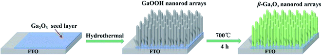 |
| | Fig. 1 Schematic illustration of preparation of the β-Ga2O3 NRAs. | |
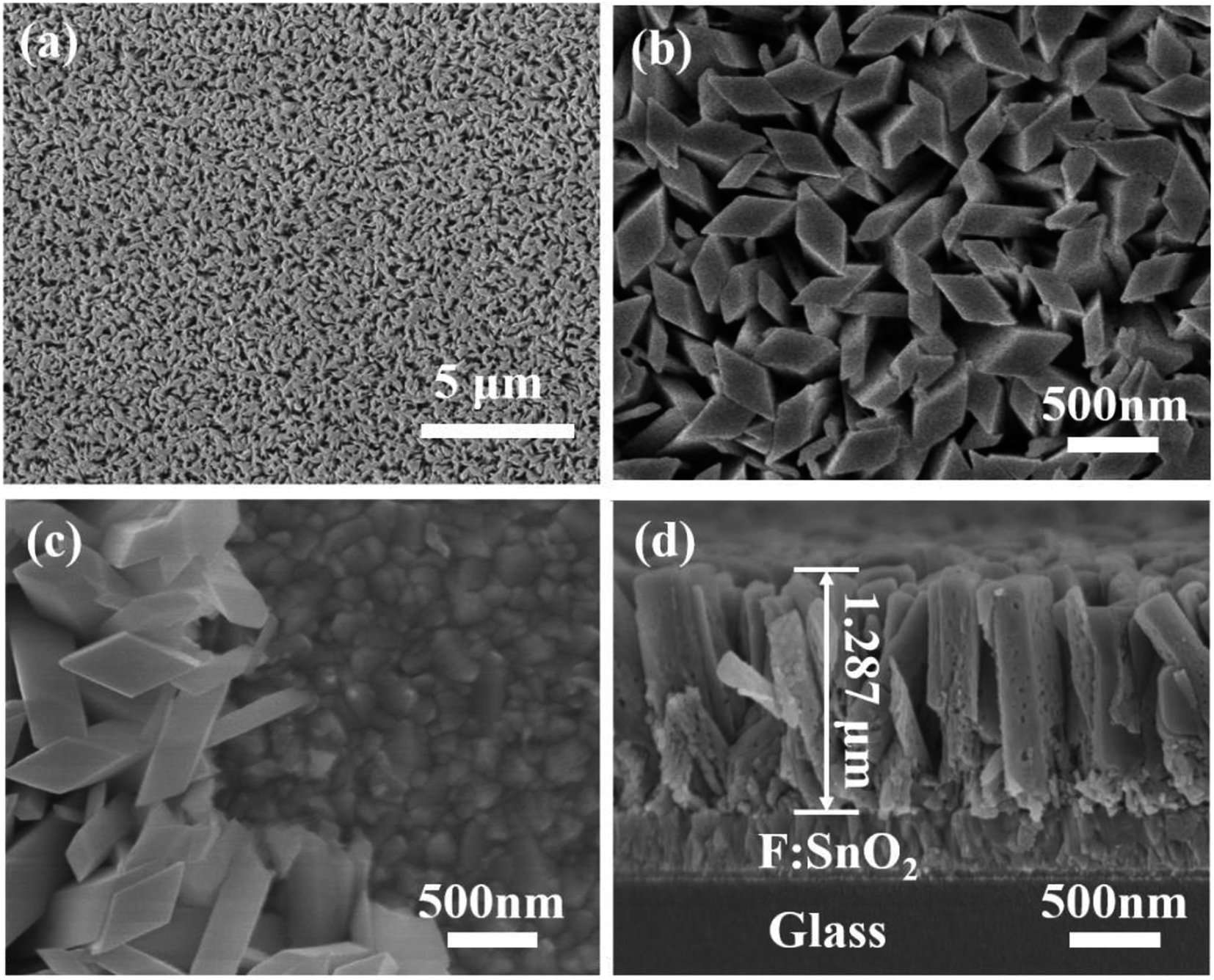
The SEM result shows that a large-area, highly dense, and vertically aligned β-Ga2O3 NRAs have been successfully grown on the FTO glass substrate [Fig. 2(a–d)]. Fig. 2(a) displays a representative top-view SEM micrograph of as-synthesized β-Ga2O3 nanorods. Fig. 2(b) is a magnified image of Fig. 2(a). Fig. 2(c) is a top view SEM image in the boundaries of NRAs. Obviously, there has a high density and flat surface of β-Ga2O3 NRAs aligned vertically grown on FTO substrate. It also can be observed that the tips of the nanorods are the diamond shape, whose diameter has changed in the range of 100 to 500 nm. Fig. 2(d) shows the cross-section image of β-Ga2O3 NRAs on FTO substrate, we can estimate that the average length of nanorods is ∼1.287 μm. Fig. 3(a) shows the XRD patterns of the FTO, FTO/GaOOH and β-Ga2O3 NRAs, respectively. In addition to the diffraction peak of the FTO substrate, four peaks located at 35.3°, 37.4°, 62.3° and 66.7° were observed in FTO/GaOOH, which can be indexed to (021), (111), (002) and (070) crystal planes of orthorhombic GaOOH (JCPDS file no. 06-0180). The NRAs show a preferred growth orientation of [111] direction. After the annealing of as-prepared GaOOH NRAs, three additional peaks located at 31.7°, 35.3° and 37.9° were observed, which can be ascribed to the (002), (111) and (401) planes of monoclinic β phase of Ga2O3 (JCPDS file no. 41-1103).25 The UV-vis absorbance spectra of the β-Ga2O3 NRAs is shown in Fig. 3(b). It shows that the absorption onset of β-Ga2O3 is at ∼270 nm. The optical bandgaps of β-Ga2O3 NRAs can be determined based on the equation: (αhν)2 = A(hν – Eg). The energy bandgap (Eg) is measured by linear extrapolation to the hν-axis. The (αhν)2 versus hν curve of the β-Ga2O3 NRAs is shown in the inset of Fig. 3(b), the band-gap of β-Ga2O3 NRAs was estimated to be ∼4.63 eV, which is almost identical with previous reports.3,20
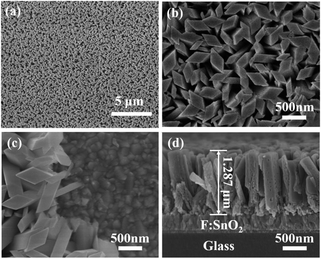 |
| | Fig. 2 The top views of SEM images at low (a) and high (b) magnification of β-Ga2O3 NRAs grown on the FTO substrate. (c) The edge view of β-Ga2O3 NRAs. (d) The cross-section of β-Ga2O3 NRAs on the FTO substrate. | |
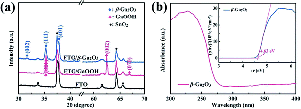 |
| | Fig. 3 (a) XRD patterns of the FTO, FTO/GaOOH NRAs and FTO/β-Ga2O3 NRAs. (b) The absorption spectrum of β-Ga2O3 nanorod, the inset is (αhν)2 versus hv. | |
A circular Ti/Au electrode was patterned on β-Ga2O3 NRAs to fabricate a solar-blind deep ultraviolet photodetector. The schematic diagram of the device is presented in Fig. 4(a). Fig. 4(b) depicts the current voltage (I–V) curves of the device in dark and under 254 nm illumination with various light densities. Obviously, under the 254 nm ultraviolet illumination, the current in the reverse bias is larger than that in the forward bias. The inset of Fig. 4(b) is the enlarged curves around zero bias. It can be seen at 0 V bias that the current of the device increases in negative direction with the increase of the light densities, exhibiting a self-powered characteristic.
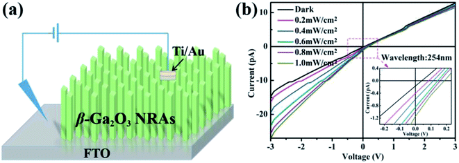 |
| | Fig. 4 (a) The schematic diagram of the β-Ga2O3 NRAs solar-blind photodetector. (b) I–V curves of the device in dark and under 254 nm illumination with various light power densities. | |
Fig. 5(a) shows the time-dependent photoresponse (I–t) of the device measured at 0 V bias under 254 nm illumination with various light intensities. It exhibits stable and reproducible characteristics under an on/off interval of 20 s. The dark current is approximately −0.18 pA. Under 254 nm light illumination, along with the light densities increased from 0.2 to 1.2 mW cm−2, the negative photocurrent value of device increase from 0.421 to 1.644 pA. The corresponding light/dark ratios (Ilight/Idark) are gradually increased from 2.34 to 9.14. Notably, the photocurrent of the device linearly increases with the increase of the light intensities, as shown in Fig. 5(b), revealing that the stronger ultraviolet light can excite more photogenerated carriers. I–t curve of self-powered β-Ga2O3 NRAs solar-blind photodetector at 0 V bias under 1.2 mW cm−2 254 nm light irradiation is enlarged in Fig. 5(c). The rising and decaying edges were fitted by an exponential relaxation equation of the following type:
| |
I = I0 + A![[thin space (1/6-em)]](https://www.rsc.org/images/entities/char_2009.gif) e−t/τ1 + Be−t/τ2 e−t/τ1 + Be−t/τ2
| (1) |
where
I0 is the steady state photocurrent,
t is the time,
A and
B are constant,
τ1 and
τ2 are two relaxation time constants.
τr and
τd are the time constants for the rising edge and fall edge, respectively. The rise time (
τr) and the decay time (
τd) of are approximately 0.64 s and 0.38 s respectively.
3 It is noticed in
Fig. 5(d) that
τr and
τd show downward trend with the increase of light intensity. The photoresponse switching behaviors of the device at different applied bias voltages were measured under 254 nm illumination as shown in
Fig. 5(e). Apparently, both the dark current and photocurrent increases along with the increase of the bias voltages ranging from 0 V to −1.5 V. Meanwhile, the photocurrent of 17.60 pA at −1.5 V is about 11 times than that at 0 V under the same conditions. Notably, the photocurrent increases linearly with the increase of the electric field, because a more separation and transportation of electron–hole pairs would excite more pairs of the photo-generated electron–hole, resulting in a higher photocurrent. Photoresponsivity (
Rλ) and external quantum efficiency (EQE) are two important parameters to evaluate the sensitivity of PDs.
Rλ is defined as the photocurrent generated by per unit power of incident light on the effective area of a PD and EQE is bound up with the number of electron–hole pairs excited by a PD per adsorbed photon and per unit time.
Rλ and EQE can be expressed in the following equations:
where Δ
Iλ =
Iλ −
Idark is the difference between photocurrent and dark current,
Pλ is the incident light intensity,
S is the effective illuminated area,
h is the Planck's constant,
c is the velocity of light, e is the electron charge, and
λ is the incident light wavelength. It can calculate that the device exhibits a photoresponsivity (
Rλ) of 10.80 mA W
−1 and an external quantum efficiency (EQE) of 5.27 × 10
−3% at 0 V bias under 1.2 mW cm
−2 254 nm illumination. Simultaneously, the
Rλ and EQE are estimated to 85.52 mA W
−1 and 4.18 × 10
−2% for −1.5 V bias, respectively. It can be seen from the
Fig. 5(f) that
Rλ increases near linearly with the bias voltage. Accordingly, applying bias voltage is a good way to rationally optimize the photoelectric performance of photodetector. For comparison, we list the photoresponse parameters of β-Ga
2O
3 NRAs PD and other types of devices reported in the literature in
Table 1. It can be seen that compared with the other type device our device can work at zero bias. The β-Ga
2O
3 NRAs PD with a simple structure renders relatively high performance, wide absorption region and low fabrication cost, promising building high performance optoelectronic devices with a self-powered worked characteristic in the future.
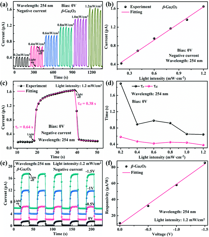 |
| | Fig. 5 (a) I–t curves of the device measured at 0 V bias under 254 nm illumination with various light intensities. (b) The relationship between the light intensity and photocurrent. (c) Rise time and decay time of the device at 0 V bias under 254 nm light irradiation with a light intensity of 1.2 mW cm−2. (d) The relationship between the light intensity and photoresponse time. (e) The photoresponse switching behaviors of the device were measured at different applied bias voltages. (f) The relationship between the light intensity and applied bias voltage. | |
Table 1 Comparison of the device parameters of the present β-Ga2O3 NRAs based photoresponse parameters and other Ga2O3 nanostructures based devices
| Materials and structure |
UV light |
Bias voltage |
R (A W −1) |
EQE (%) |
Reference |
| Ga2O3 nanorods |
254 |
0.33 |
19.31 |
9427 |
24 |
| Ga2O3 nanowire |
255 |
5 |
3.43 × 10⁻³ |
1.37 |
25 |
| GaOOH nanorod |
254 |
0.5 |
1.07 |
522 |
26 |
| Ga2O3 nanorods |
254 |
0 |
1.08 × 10⁻² |
5.27 × 10⁻³ |
This work |
4. Conclusions
In conclusion, a self-powered solar-blind photodetector was successfully fabricated by simple and low cost β-Ga2O3 NRAs growth process. The fabricated β-Ga2O3 NRAs based PD showed an obvious photoresponse in solar-blind ultraviolet region with good repeatability and stability. Under 0 V bias and 1.2 mW cm−2 254 nm illumination, the photodetector exhibits a Ilight/Idark ratio of 9.14, a Rλ of 10.80 mA W−1, τr of 0.64 s and τd of 0.38 s. The self-powered photodetector based on β-Ga2O3 NRAs with high light-to-electron conversion and low power consumption abilities is a promising candidate for solar-blind photodetection application.
Conflicts of interest
There are no conflicts to declare.
Acknowledgements
This work was supported by the National Natural Science Foundation of China (No. 61704153, 51572241, 61774019, 51572033, 11605149), Zhejiang Public Service Technology Research Program/Analytical Test (LGC19F040001), Open Fund of IPOC (BUPT), and Science and Technology Department of Zhejiang Province Foundation (2017C37017).
References
- L. W. Sang, M. Y. Liao and M. Sumiya, et al., A comprehensive review of semiconductor ultraviolet photodetectors: from thin film to one-dimensional nanostructures, Sensors, 2013, 13(8), 10482–10518 CrossRef CAS PubMed
 .
. - D. S. Tsai, W. C. Lien and D. H. Lien, et al., Solar-blind photodetectors for harsh electronics, Sci. Rep., 2013, 4(9), 2628 CrossRef PubMed .
- B. Zhao, F. Wang and H. Y. Chen, et al., Solar-blind avalanche photodetector based on single ZnO–Ga2O3 core–shell microwire, Nano Lett., 2015, 15(6), 3988 CrossRef CAS PubMed .
- Q. Zhang, J. S. Jie and S. L. Diao, et al., Solution-processed graphene quantum dot deep-UV photodetectors, ACS Nano, 2015, 9(2), 1561–1570 CrossRef CAS PubMed .
- N. Shouleh, H. Michael and D. J. April, et al., Single photon counting UV solar-blind detectors using silicon and III-nitride materials, Sensors, 2016, 16(6), 927 CrossRef PubMed .
- C. Y. Cho, Y. Zhang and E. Cicek, et al., Surface plasmon enhanced light emission from AlGaN-based ultraviolet light-emitting diodes grown on Si (111), Appl. Phys. Lett., 2013, 102, 211110 CrossRef .
- F. H. Teherani, D. C. Look and D. J. Rogers, et al., Optical properties of ZnMgO films grown by spray pyrolysis and their application to UV photodetection, Semicond. Sci. Technol., 2015, 30(10), 105026 CrossRef .
- X. C. Guo, N. H. Hao and D. Y. Guo, et al., β-Ga2O3/p-Si heterojunction solar-blind ultraviolet photodetector with enhanced photoelectric responsivity, J. Alloys Compd., 2016, 660, 136–140 CrossRef CAS .
- K. W. Liu, M. Sakurai and M. Aono, ZnO-based ultraviolet photodetectors, Sensors, 2010, 10, 8604–8634 CrossRef CAS PubMed .
- L. K. Wang, Z. G. Ju and J. Y. Zhang, et al., Single-crystalline cubic MgZnO films and their application in deep-ultraviolet optoelectronic devices, Appl. Phys. Lett., 2009, 95, 131113 CrossRef .
- X. L. Du, Z. X. Mei and Z. L. Liu, et al., Controlled growth of high-quality ZnO-based films and fabrication of visible-blind and solar-blind ultra-violet detectors, Adv. Mater., 2009, 21, 4625–4630 CrossRef CAS .
- Y. P. Qian, D. Y. Guo and X. L. Chu, et al., Mg-doped p-type β-Ga2O3 thin film for solar-blind ultraviolet photodetector, Mater. Lett., 2017, 209, 558–561 CrossRef CAS .
- D. Y. Guo, X. L. Zhao and Y. S. Zhi, et al., Epitaxial growth and solar-blind photoelectric properties of corundum-structured α-Ga2O3 thin films, Mater. Lett., 2016, 164, 364–367 CrossRef CAS .
- D. Y. Guo, Y. L. Su and H. Z. Shi, et al., Self-powered ultraviolet photodetector with super high photoresponsivity (3.05 A/W) based on the GaN/Sn:Ga2O3 pn junction, ACS Nano, 2018, 12, 12827–12835 CrossRef CAS PubMed .
- D. Y. Guo, H. Liu and P. G. Li, et al., Zero-power-consumption solar-blind photodetector based on β-Ga2O3/NSTO heterojunction, ACS Appl. Mater. Interfaces, 2017, 9(2), 1619–1628 CrossRef CAS PubMed .
- D. Y. Guo, H. Z. Shi and Y. P. Qian, et al., Fabrication of β-Ga2O3/ZnO heterojunction for solar-blind deep ultraviolet photodetection, Semicond. Sci. Technol., 2017, 32(3), 03LT01 CrossRef .
- D. Y. Guo, Z. P. Wu and P. G. Li, et al., Fabrication of β-Ga2O3 thin films and solar-blind photodetectors by laser MBE technology, Opt. Mater. Express, 2014, 4(5), 1067 CrossRef .
- L. P. Dong, R. X. Jia and C. Li, et al., Ab initio study of N-doped β-Ga2O3 with intrinsic defects: the structural, electronic and optical properties, J. Alloys Compd., 2017, 712, 379–385 CrossRef CAS .
- H. P. Zhang, R. X. Jia and L. Yuan, et al., Leakage current conduction mechanisms and electrical properties of atomic-layer-deposited HfO2/Ga2O3 MOS capacitors, J. Phys. D: Appl. Phys., 2018, 51(7), 1 Search PubMed .
- T. He, Y. K. Zhao and X. D. Zhang, Solar-blind ultraviolet photodetector based on graphene/vertical Ga2O3 nanowire array heterojunction, Nanophotonics, 2018, 7, 1557 CAS .
- H. O. Li, Y. Li and G. L. Xiao, et al., Simple fabrication ZnO/β-Ga2O3 core/shell nanorod arrays and their photoresponse properties, Opt. Mater. Express, 2018, 8, 794 CrossRef .
- W. W. Zhong, S. J. Shen and S. S. Feng, et al., Facile fabrication of alveolate Cu2–xSe microsheets as a new visible-light photocatalyst for discoloration of Rhodamine B, CrystEngComm, 2018, 20, 7851 RSC .
- W. W. Zhong, W. G. Tu and S. S. Feng, et al., Photocatalytic H2 evolution on CdS nanoparticles by loading FeSe nanorods as co-catalyst under visible light irradiation, J. Alloys Compd., 2019, 772, 669–674 CrossRef CAS .
- Y. L. Wu, S. J. Chang and W. Y. Weng, et al., Ga2O3 nanowire photodetector prepared on SiO2/Si template, IEEE Sens. J., 2013, 13, 2368–2373 CAS .
- H. J. Lin, J. P. Baltrus and H. Y. Gao, et al., Perovskite nanoparticle-sensitized Ga2O3 nanorod arrays for CO detection at high temperature, ACS Appl. Mater. Interfaces, 2016, 8, 8880 CrossRef CAS PubMed .
- K. Chen, C. R. He and D. Y. Guo, et al., Low-voltage-worked photodetector based on Cu2O/GaOOH shell-core heterojunction nanorod arrays, J. Alloys Compd., 2018, 755, 199–205 CrossRef CAS .
Footnote |
| † These authors contributed equally to this work. |
|
| This journal is © The Royal Society of Chemistry 2019 |
Click here to see how this site uses Cookies. View our privacy policy here. 
 Open Access Article
 This Open Access Article is licensed under a Creative Commons Attribution-Non Commercial 3.0 Unported Licence
 a,
Daoyou Guo
a,
Daoyou Guo