 Open Access Article
Creative Commons Attribution 3.0 Unported Licence
Thermoelectric properties of n-type Cu4Sn7S16-based compounds†
Tingting Dengabc,
Tian-Ran Wei *a,
Qingfeng Songab,
Qing Xuabc,
Dudi Rena,
Pengfei Qiu
 a,
Xun Shi
 *a and
Lidong Chena
aState Key Laboratory of High Performance Ceramics and Superfine Microstructure, Shanghai Institute of Ceramics, Chinese Academy of Sciences, Shanghai 200050, China. E-mail: wtr@mail.sic.ac.cn; xshi@mail.sic.ac.cn
bCenter of Materials Science and Optoelectronics Engineering, University of Chinese Academy of Sciences, Beijing 100049, China
cSchool of Physical Science and Technology, ShanghaiTech University, Shanghai 201210, China
First published on 8th March 2019
Abstract
Copper-based chalcogenides have ultralow thermal conductivity and ultrahigh thermoelectric performance, but most of them are p-type semiconductors. It is urgent to develop n-type counterparts for high efficiency thermoelectric modules based on these copper based-chalcogenides. Cu4Sn7S16 is an intrinsically n-type semiconductor with complex crystal structure and low thermal conductivity. However, its thermoelectric properties have not been well studied when compared to the well-known n-type CuFeS2. In this work, high-quality Cu4Sn7S16-based compounds are fabricated and their thermoelectric properties are systematically studied. Using Ag and Sb as dopants, the carrier concentration is tuned over a wide range. The electrical transport properties can be well described by the single parabolic band model with carrier acoustic phonons scattering. It is revealed that Cu4Sn7S16 exhibits a low effective mass and relatively high mobility. The thermal conductivity is lower than 0.8 W m−1 K−1 from 300 to 700 K and shows a weak dependence on temperature. A maximum zT of 0.27 is obtained in Cu3.97Ag0.03Sn7S16 at 700 K. Further enhancement of thermoelectric performance is possible when a more efficient n-type dopant is used.
Introduction
Thermoelectric (TE) materials are able to realize the direct conversion between heat and electricity. The conversion efficiency depends mainly on the dimensionless figure of merit zT = S2σT/κ, where S is the Seebeck coefficient, σ is the electrical conductivity, T is the absolute temperature and κ is the thermal conductivity.1–4 In recent years, Cu-based TE materials have emerged as promising thermoelectric materials not only for the large abundance and low-toxicity of the elements, but also for the diverse structure and lattice dynamics, interesting transport properties and high thermoelectric performance.5–8It has been realized that most of the Cu-based TE materials are p-type semiconductors probably due to the intrinsic Cu vacancies that have a low formation energy,9 such as Cu2X (X = S, Se, Te),10 diamond-like compounds11 and their derivatives.12 However, a TE device is composed of both p-type and n-type legs. Also, the p- and n-type counterparts should match each other in electrical, thermal and mechanical properties and operation temperatures. Therefore, it is crucial to develop high-efficiency, compatible n-type Cu-based materials for application.
So far, there are only a few n-type Cu-based TE compounds reported probably due to the prevalent presence of intrinsic Cu vacancies. The current n-type copper chalcogenides are mainly ternary sulfides where S vacancies may compete with Cu vacancies, acting as donors. CuFeS2, i.e. the well-known chalcopyrite, exhibits a maximum zT of ∼0.2 with a high lattice thermal conductivity (∼5.9 W m−1 K−1) and a low carrier mobility (∼3.0 cm2 V−1 s−1).13 A lot of studies have been carried out on this compound, providing an insight into the crystal structure, phase variation, transport behaviour and underlying mechanisms as well as synthesis techniques.13–16 Another compound CuFe2S3 tends to decompose into CuFeS2 and Fe7S8 at room temperature.17 Besides, Cu5FeS4 exhibits an n–p transition around 450 K due to the intrinsic excitation.18 The compound Cu4Sn7S16, a largely distorted derivative of diamond-like materials, possesses a complex crystal structure (Fig. 1) with a very large cell volume 1694.8 Å3 and 81 atoms per unit cell,19 which is likely to result in a low lattice thermal conductivity favorable to thermoelectric performance.20
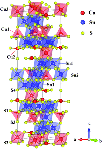 | ||
| Fig. 1 Crystal structure of Cu4Sn7S16. The crystallographic parameters are taken from ref. 19. | ||
Previous studies20,21 have shown that Cu4Sn7S16 exhibits a pretty low thermal conductivity (∼1 W m−1 K−1 at 300 K) and high Seebeck coefficient varying from −200 to −750 μV K−1 depending on the synthesis processes, suggesting the potential of this compound as a promising n-type Cu-based TE material. In 2015, Bourgès et al. reported an optimized zT of 0.2 at 600 K.20 The main barrier limiting TE performance of Cu4Sn7S16 is its low electrical conductivity, about 10−3 to 103 S m−1 at room temperature,19–21 which is far lower than conventional TE materials (104 to 105 S m−1).22 Therefore, feasible doping is needed to optimize the electrical properties, which has rarely been conducted. Recently, Cui et al. found that excess Sn and Se substitution for S can enhance zT up to 0.5 at a relatively high temperature of 873 K.23,24 Nonetheless, the carrier concentration is limited to the order of 1016 cm−3 in their work, and a deep insight into the electrical transports is needed based on the samples of a wide range of carrier density.
In this work, we synthesized high-purity Cu4Sn7S16-based compounds and studied their electrical and thermal transports as well as the doping effects. Using Sb and Ag as dopants, the carrier concentration was tuned from 2.1 × 1017 cm−3 to 6.7 × 1018 cm−3. The electrical transport properties can be reasonably described by the single parabolic band model. When compared with CuFeS2, the compound Cu4Sn7S16 was found to have a higher mobility due to the absence of d electrons from Fe and a lower thermal conductivity benefiting from the complex crystal structure. A maximum zT = 0.27 was achieved at 700 K in Ag-doped Cu4Sn7S16.
Experimental
Pristine Cu4Sn7S16 and Sb-, Ag-doped samples were synthesized by the conventional melting-annealing method as described elsewhere.20 High-purity raw materials of Cu (shots, 99.999%, Alfa Aesar), Ag (shots, 99.999%, Alfa Aesar), Sn (shots, 99.999%, Alfa Aesar), Sb (shots, 99.999%, Alfa Aesar) and S (pieces, 99.999%, Alfa Aesar) were weighed out according to the stoichiometric ratio, and sealed in quartz tubes under vacuum in the glove box filled with argon. The tubes were put into the vertical furnace (NaberTherm). The furnace was heated to 723 K in 4.5 hours and held at this temperature for 2 hours, then heated to 1123 K in 4 hours and kept at this temperature for 2 hours. Then the temperature was decreased to 973 K in 1.5 hours and kept at this temperature for 2 days. The ingots were then fully ground in the agate mortar, pelletized, sealed into quartz tubes, and annealed at 973 K for 3 days. Finally, the products were ground into powders and sintered at 923 K under a uniaxial pressure of 65 MPa for 15 minutes by Spark Plasma Sintering (Sumitomo, SPS-2040). The sintering was carried out in argon atmosphere, and the pressure is about 0.07 MPa. The relative densities of all samples are around 99% measured by the Archimedes method.The phase purity and crystal structure were detected by X-ray diffraction with Cu Kα sources (XRD, D/max-2550 V, Rigaku, Japan). Transmission electron microscopy (TEM, JEM-2100F, Japan) and selected area electron diffraction (SAED) were used to check the crystal structure. The distribution of chemical composition was characterized by scanning electron microscopy (SEM, ZEISS supra 55, Germany) and Energy Dispersive X-ray Spectroscopy (EDS, Oxford, UK) with accelerate voltage set as 20 kV. X-ray photoelectron spectroscopy (XPS, ESCALAB250, USA) was used to analyze the valence state of main elements in the samples, and the sample surface was sputtered by Ar+ beam before testing (2 kV, 20 s). The electrical conductivity (σ) and Seebeck coefficient (S) were measured from 300 K to 700 K by using ZEM-3 (Ulvac-Riko Japan). The Hall coefficient (RH) was measured at room temperature by Physical Property Measurement System (PPMS, Quantum Design, USA). The optical diffuse reflectance (R) was conducted on powder samples by using the UV-Vis spectrum (Shimadzu Spectroscope, UV-3101PC, Japan) at room temperature. The optical energy gap (Eg) was obtained based on the Kubelka–Munk method by extrapolating (1 − R)2/2R to 0 as a function of hυ (where hυ is photon energy).25 The thermal conductivity was derived from the formula κ = ρCpλ, where ρ is the density, Cp is the isobaric heat capacity estimated according to the Dulong–Petit law, λ is thermal diffusivity measured by using the Laser flash method (LFA457, Netzsch, Germany). The velocity of sound (v) was measured by using the Advanced Ultrasonic measurement system (UMS, TECLAB, France).
Results and discussion
Cu4Sn7S16 crystallizes into a rhombohedral structure with the space group of R![[3 with combining macron]](https://www.rsc.org/images/entities/char_0033_0304.gif) m (no. 166, Z = 3) as shown in Fig. 1, where sulfur atoms (S1, S2, S3 and S4) form the frameworks of tetrahedrons and octahedrons. Three kinds of octahedral sites are occupied by Sn1, Sn2 and Cu3, and two tetrahedral sites are totally and half occupied by Cu2 and Cu1, respectively. Also, it is suggested that Cu2 and Cu3 atoms exhibit a large displacement,19,21 possibly contributing to the low thermal conductivity.20,26
m (no. 166, Z = 3) as shown in Fig. 1, where sulfur atoms (S1, S2, S3 and S4) form the frameworks of tetrahedrons and octahedrons. Three kinds of octahedral sites are occupied by Sn1, Sn2 and Cu3, and two tetrahedral sites are totally and half occupied by Cu2 and Cu1, respectively. Also, it is suggested that Cu2 and Cu3 atoms exhibit a large displacement,19,21 possibly contributing to the low thermal conductivity.20,26
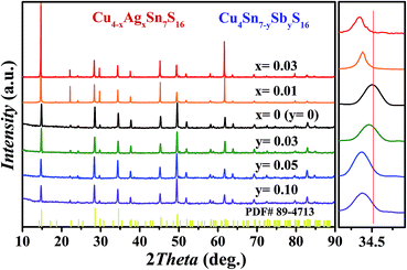
As shown in Fig. 2, all the samples were identified as Cu4Sn7S16 with the rhombohedral structure (R![[3 with combining macron]](https://www.rsc.org/images/entities/char_0033_0304.gif) m, PDF#89-4713) and no secondary phases were found when x ≤ 0.03 or y ≤ 0.10. Impurity phases emerge when the doping contents exceed these ranges (Fig. S1 and S2 in ESI†). The diffraction peaks shift slightly to the lower angles with increased Sb and Ag content. The Rietveld refinement results and the lattice constants (Fig. S3 and Table S1 in ESI†) confirm that the lattice volume expands upon Sb and Ag doping. These results indicate that the dopants have entered the lattice.
m, PDF#89-4713) and no secondary phases were found when x ≤ 0.03 or y ≤ 0.10. Impurity phases emerge when the doping contents exceed these ranges (Fig. S1 and S2 in ESI†). The diffraction peaks shift slightly to the lower angles with increased Sb and Ag content. The Rietveld refinement results and the lattice constants (Fig. S3 and Table S1 in ESI†) confirm that the lattice volume expands upon Sb and Ag doping. These results indicate that the dopants have entered the lattice.
Fig. 3(a) shows the high-resolution TEM images of Cu4Sn7S16 and the inset is the fast Fourier transformation (FFT) for the entire area. The distances of crystal planes (0![[1 with combining macron]](https://www.rsc.org/images/entities/char_0031_0304.gif)
![[2 with combining macron]](https://www.rsc.org/images/entities/char_0032_0304.gif) ), (1
), (1![[1 with combining macron]](https://www.rsc.org/images/entities/char_0031_0304.gif)
![[4 with combining macron]](https://www.rsc.org/images/entities/char_0034_0304.gif) ) and (10
) and (10![[2 with combining macron]](https://www.rsc.org/images/entities/char_0032_0304.gif) ) are 6.10 Å, 5.23 Å and 6.10 Å, respectively in Fig. 3(b) and (c), being well consistent with the standard diffraction data. The selected area electron diffraction pattern in Fig. 3(d) is clean and clear without any splitting, and agrees well with the FFT in Fig. 3(a), confirming the good crystallinity of the sample. It is worth mentioning that twinings were observed by Bourgès et al.20 Although we use the same sample fabrication process as Bourgès, the sintering temperature and holding time for final bulk samples are different. The difference in synthesis condition might lead to different microstructures and lattice defects. As shown in Fig. 4, the EDS images reveal that there are no visible impurities at micron scales, and the main elements exhibit a uniform distribution.
) are 6.10 Å, 5.23 Å and 6.10 Å, respectively in Fig. 3(b) and (c), being well consistent with the standard diffraction data. The selected area electron diffraction pattern in Fig. 3(d) is clean and clear without any splitting, and agrees well with the FFT in Fig. 3(a), confirming the good crystallinity of the sample. It is worth mentioning that twinings were observed by Bourgès et al.20 Although we use the same sample fabrication process as Bourgès, the sintering temperature and holding time for final bulk samples are different. The difference in synthesis condition might lead to different microstructures and lattice defects. As shown in Fig. 4, the EDS images reveal that there are no visible impurities at micron scales, and the main elements exhibit a uniform distribution.
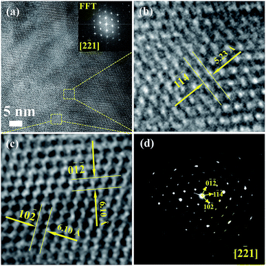 | ||
| Fig. 3 (a)–(c) HRTEM images for Cu4Sn7S16, and the inset picture of (a) is the fast Fourier transformation (FFT) image; (d) selected area electron diffraction pattern (SAED). | ||
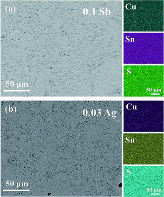 | ||
| Fig. 4 Backscattered electron (BSE) and EDS patterns of (a) Cu4Sn6.9Sb0.1S16 and (b) Cu3.97Ag0.03Sn7S16. | ||
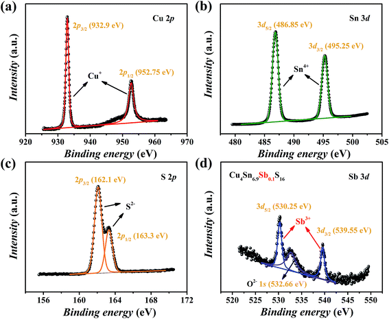
The XPS spectra of Cu4Sn6.9Sb0.1S16 are shown in Fig. 5. The valence states of main elements Cu, Sn and S were identified as 1+, 4+ and 2−, respectively, which agrees with the available studies19,23 on Cu4Sn7S16. The binding energies of Sb were found to be 530.25 eV for 3d5/2 and 539.55 eV for 3d3/2 orbitals with a doublet separation (DS) of 9.3 eV (Fig. 5(d)), which is close to the data of Sb3+-containing materials such as Sb2S3 (BE: 529.6 eV for 3d5/2 and 539 eV for 3d3/2; DS: 9.4 eV),27 CuSbS2 (BE: 529.03 eV for 3d5/2 and 538.43 eV for 3d3/2; DS: 9.4 eV),28 and Cu12Sb4S13 (BE: 539.0 eV for 3d3/2).29 Therefore, the substitution of Sb3+ for Sn4+ is expected to generate extra holes.
The measured Hall carrier concentration nH is shown in Fig. 6(a). nH is 4.1 × 1018 cm−3 at 300 K for the undoped Cu4Sn7S16, being on the same order of magnitude of the reported data (9.2 × 1018 cm−3).20 nH decreases with increasing Sb content to 0.1, confirming that Sb is a p-type dopant as predicted by XPS. In contrast, Ag doping slightly enhances nH. This is in line with the common phenomena that Ag-based chalcogenides tend to show n-type conduction,30–33 which is probably related to the formation of more S vacancies or Ag interstitial atoms. The carrier mobility is 34 cm2 V−1 s−1 for undoped sample and does not change much when doped (Fig. 6(b)).
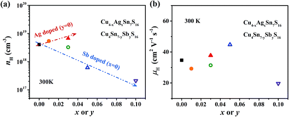 | ||
| Fig. 6 (a) Hall carrier concentration (nH) and (b) Hall carrier mobility (μH) at room temperature against the contents of Ag and Sb. The arrows in (a) represent the trend of change. | ||
The electrical conductivity of the pristine sample decreases from 2.3 × 10³ S m−1 at 300 K to 1 × 10³ S m−1 at 700 K as shown in Fig. 7(a). σ decreases when doped with Sb and increases with Ag, which agrees with the change of nH. All samples exhibit negative Seebeck coefficients in the entire measured temperature range, confirming the n-type conduction. The absolute values of S for all samples are relatively large, over 200 μV K−1, increasing with Sb content and decreasing with Ag content (Fig. 7(b)). According to the Eg = 2eSmaxTSmax relation,34 the band gap was estimated to be 0.54 eV, which is reasonably consistent with the measured optical gap (0.63 eV, inset of Fig. 7(b)). The power factor (PF) changes in keeping with the carrier concentration (Fig. 7(c) and (f)).
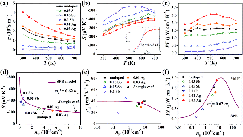 | ||
Fig. 7 Temperature dependence of (a) electrical conductivity, (b) Seebeck coefficient and (c) power factor of all samples from 300 K to 700 K; the inset pattern in (b) represents the optical band gap of pristine Cu4Sn7S16. (d) Seebeck coefficient, (e) Hall mobility and (f) power factor varying with Hall carrier concentration at 300 K; the solid curves were calculated based on the single parabolic band (SPB) model with  . The data of ref. 20 were also given for comparison. . The data of ref. 20 were also given for comparison. | ||
In order to get an insight into the electrical transport properties of this compound, the single parabolic band (SPB) model was employed, and it was assumed that carriers are dominantly scattered by acoustic phonons. The transport parameters can be written as:35
 | (1) |
 | (2) |
 | (3) |
| PF = S2nHμHe | (4) |
 ,
,  is the density-of-state (DOS) effective mass, kB is the Boltzmann constant, h is the Planck constant, μ0 is the mobility at the nondegenerate limit that was fitted to be 45 cm2 V−1 s−1. As shown in Fig. 7(d), the fitting line with
  was found adequate to describe the dependence of Seebeck coefficient on the carrier concentration. Such a small
  is consistent with previous studies (∼0.73 me),20 and may be related to the delocalized electrons from the sp orbitals of Sn. The small effective mass directly brings about a relatively high carrier mobility of 34 cm2 V−1 s−1 for undoped sample (Fig. 7(e)), being significantly larger than CuFeS2 (3.0–13.9 cm2 V−1 s−1).13,14,16 As shown in Fig. 7(f), the experimental data fall well on the theoretical line. The optimal carrier concentration is about 2 × 1019 cm−3 at room temperature, which is slightly higher than the one achieved in this work.
For pristine Cu4Sn7S16, κ fluctuates from ∼0.8 W m−1 K−1 at room temperature (RT) to ∼0.55 W m−1 K−1 at 700 K (Fig. 8(a)). In contrast to the electrical properties, there is no obvious change in κ considering the small number of dopants. Due to the relatively low electrical conductivity, the lattice thermal conductivity κL accounts for >95% of the total κ. Such a low κL originates from the intrinsically complex crystal structure. Specifically, acoustic phonons are not only scattered by the Umklapp process (κL ∝ T−1),36 but also by the point defects (half occupation of Cu1 sites) and possible optical resonant modes arising from the large vibration of certain Cu atoms as widely found in Cu- and Ag-based chalcogenides.33,37 The relationship between the crystal structure, lattice dynamics, phonon dispersion and thermal transports will be comprehensively studied in the future. As shown in Fig. 8(b), zT is 0.18 at 700 K in undoped Cu4Sn7S16. When the content of Ag is 0.03 (Cu3.97Ag0.03Sn7S16), the optimal zT was enhanced to 0.27, which is 50% higher than the pristine one and also higher than the previous studies20,23,24 at the same temperature.
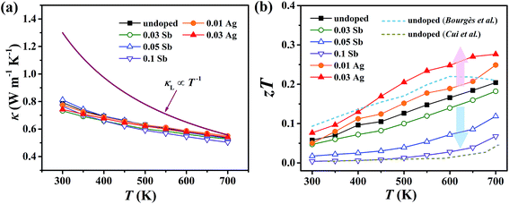 | ||
| Fig. 8 Temperature dependence of (a) total thermal conductivity (κ) and (b) figure of merit (zT). Blue and yellow dash lines represent the data taken from ref. 20 and 24, respectively. | ||
It is interesting to compare the two n-type Cu-based thermoelectric chalcogenides: Cu4Sn7S16 and CuFeS2. The elastic parameters of the two compounds were derived based on the measured sound velocity. The average sound velocity (vs) was calculated by38,39
 | (5) |
 | (6) |
 | (7) |
 | (8) |
As shown in Table 1, the elastic parameters of the two compounds are comparable to each other, corresponding to the lowest lying acoustic phonon characters and intrinsic Umklapp process. Nonetheless, the κL of Cu4Sn7S16 is only 1/7 of that in CuFeS2, which originates from the complex crystal structure of the former. For electrical transports, the mobility of Cu4Sn7S16 is higher than CuFeS2 by an order of magnitude, which is probably related to the absence of valence electrons from the relatively localized d orbitals of Fe while the conduction band minimum (CBM) of CuFeS2 is mainly from the contribution of Fe 3d orbitals.43 The challenge for CuFeS2 lies in suppressing the κ while it is crucial to find more efficient n-type dopants for Cu4Sn7S16.
| CuFeS2a | Cu4Sn7S16 | |
|---|---|---|
| a Most of the parameters of CuFeS2 are taken from ref. 13.b Estimated according to the Dulong–Petit law.c Calculated by the Rietveld refinements. | ||
| Formula weight | 183.53 | 1598.19 |
| Space group | I![[4 with combining macron]](https://www.rsc.org/images/entities/char_0034_0304.gif) 2d 2d |
R![[3 with combining macron]](https://www.rsc.org/images/entities/char_0033_0304.gif) m m |
| Z | 4 | 3 |
| Vcell (Å3) | 291.75 | 1697.9c |
| d (g cm−3) | 4.19 | 4.70 |
| Cp (J g−1 K−1)b | 0.14 | 0.42 |
| vs (m s−1) | 2293 | 2775 |
| vl (m s−1) | 3764 | 4625 |
| vt (m s−1) | 2056 | 2485 |
| ΘD (K) | 259 | 300 |
 |
1.2 | 0.62 |
| γ | 1.7 | 1.8 |
| Eg (eV) | 0.34 | 0.63 |
| κL (W m−1 K−1) | 5.9 | 0.78 |
| σ (S m−1) | 2.3 × 10³ | 2.5 × 10³ |
| S (μV K−1) | −370 | −260 |
| nH (cm−3) | 3.4 × 10¹⁹ | 4.0 × 10¹⁸ |
| μH (cm2 V−1 s−1) | 3.0 | 34 |
Conclusions
In this work, high-quality n-type Cu4Sn7S16-based compounds have been synthesized by the conventional melt-annealing method. The pristine material shows a large Seebeck coefficient and low electrical conductivity. The carrier concentration is tuned within a large range of 2.1 × 10¹⁷ to 6.7 × 1018 cm−3 by Ag- and Sb-doping. The electrical transports of Cu4Sn7S16 are well captured by the SPB model. Cu4Sn7S16 exhibits a low effective mass of 0.62 me and relatively high mobility of ∼34 cm2 V−1 s−1, which is ascribed to the delocalized character of sp orbitals and is in sharp contrast to 3d electrons of Fe in CuFeS2. The lattice thermal conductivity is lower than 0.8 W m−1 K−1 above room temperature, and shows a weak dependence on temperature. Maximum zT of 0.27 is obtained in Cu3.97Ag0.03Sb7S16 at 700 K. Considering the intrinsically low thermal conductivity and decent mobility, the performance of this compound can be further enhanced by more efficient doping. The findings and analyses in this work will promote the understanding on thermoelectric transports of Cu4Sn7S16-based compounds and the development of n-type Cu-based thermoelectric materials.Conflicts of interest
There are no conflicts to declare.Acknowledgements
This work is supported by the National Key Research and Development Program of China (2018YFB0703600), the National Natural Science Foundation of China (51625205, 51872314, 51802333), the Key Research Program of Chinese Academy of Sciences (KFZD-SW-421), and the Shanghai Government (16520721400).References
- G. J. Snyder and E. S. Toberer, Nat. Mater., 2008, 7, 105–114 CrossRef CAS PubMed.
- X. Shi, L. Chen and C. Uher, Int. Mater. Rev., 2016, 61, 379–415 CrossRef CAS.
- G. Tan, L. Zhao and M. G. Kanatzidis, Chem. Rev., 2016, 116, 12123–12149 CrossRef CAS PubMed.
- T. Zhu, Y. Liu, C. Fu, J. P. Heremans, G. J. Snyder and X. Zhao, Adv. Mater., 2017, 29, 1605884 CrossRef PubMed.
- H. Liu, X. Shi, F. Xu, L. Zhang, W. Zhang, L. Chen, Q. Li, C. Uher, T. Day and G. J. Snyder, Nat. Mater., 2012, 11, 422–425 CrossRef CAS PubMed.
- J. Zhang, R. Liu, N. Cheng, Y. Zhang, J. Yang, C. Uher, X. Shi, L. Chen and W. Zhang, Adv. Mater., 2014, 26, 3848–3853 CrossRef CAS PubMed.
- P. Qiu, M. T. Agne, Y. Liu, Y. Zhu, H. Chen, T. Mao, J. Yang, W. Zhang, S. M. Haile, W. G. Zeier, J. Janek, C. Uher, X. Shi, L. Chen and G. J. Snyder, Nat. Commun., 2018, 9, 2910 CrossRef PubMed.
- Y. Liu, P. Qiu, H. Chen, R. Chen, X. Shi and L. Chen, J. Inorg. Mater., 2017, 32, 1337–1344 CrossRef.
- S. Chen, A. Walsh, X. Gong and S. Wei, Adv. Mater., 2013, 25, 1522–1539 CrossRef CAS PubMed.
- K. Zhao, A. B. Blichfeld, H. Chen, Q. Song, T. Zhang, C. Zhu, D. Ren, R. Hanus, P. Qiu, B. B. Iversen, F. Xu, G. J. Snyder, X. Shi and L. Chen, Chem. Mater., 2017, 29, 6367–6377 CrossRef CAS.
- G. Zhou and D. Wang, Phys. Chem. Chem. Phys., 2016, 18, 5925–5931 RSC.
- T.-R. Wei, C.-F. Wu, W. Sun, Y. Pan and J.-F. Li, RSC Adv., 2015, 5, 42848–42854 RSC.
- Y. Li, T. Zhang, Y. Qin, T. Day, G. J. Snyder, X. Shi and L. Chen, J. Appl. Phys., 2014, 116, 203705 CrossRef.
- J. Li, Q. Tan and J.-F. Li, J. Alloys Compd., 2013, 551, 143–149 CrossRef CAS.
- W. D. Carr and D. T. Morelli, J. Electron. Mater., 2015, 45, 1346–1350 CrossRef.
- H. Xie, X. Su, G. Zheng, T. Zhu, K. Yin, Y. Yan, C. Uher, M. G. Kanatzidis and X. Tang, Adv. Energy Mater., 2017, 7, 1601299 CrossRef.
- T. Barbier, D. Berthebaud, R. Frésard, O. I. Lebedev, E. Guilmeau, V. Eyert and A. Maignan, Inorg. Chem. Front., 2017, 4, 424–432 RSC.
- P. Qiu, T. Zhang, Y. Qiu, X. Shi and L. Chen, Energy Environ. Sci., 2014, 7, 4000–4006 RSC.
- X. A. Chen, H. Wada, A. Sato and M. Mieno, J. Solid State Chem., 1998, 139, 144–151 CrossRef CAS.
- C. Bourgès, P. Lemoine, O. I. Lebedev, R. Daou, V. Hardy, B. Malaman and E. Guilmeau, Acta Mater., 2015, 97, 180–190 CrossRef.
- J. P. F. Jemetio, P. Zhou and H. Kleinke, J. Alloys Compd., 2006, 417, 55–59 CrossRef CAS.
- Materials Aspect of Thermoelectricity, ed. C. Uher, CRC Press, Boca Raton, 2017 Search PubMed.
- T. He, N. Lin, Z. Du, Y. Chao and J. Cui, J. Mater. Chem. C, 2017, 5, 4206–4213 RSC.
- J. Cui, T. He, Z. Han, X. Liu and Z. Du, Sci. Rep., 2018, 8, 8202 CrossRef PubMed.
- R. López and R. Gómez, J. Sol-Gel Sci. Technol., 2011, 61, 1–7 CrossRef.
- P. Lemoine, C. Bourgès, T. Barbier, V. Nassif, S. Cordier and E. Guilmeau, J. Solid State Chem., 2017, 247, 83–89 CrossRef CAS.
- M. Pal, N. R. Mathews and X. Mathew, J. Mater. Res., 2016, 32, 530–538 CrossRef.
- C. Macías, S. Lugo, Á. Benítez, I. López, B. Kharissov, A. Vázquez and Y. Peña, Mater. Res. Bull., 2017, 87, 161–166 CrossRef.
- R. Chetty, A. Bali, M. H. Naik, G. Rogl, P. Rogl, M. Jain, S. Suwas and R. C. Mallik, Acta Mater., 2015, 100, 266–274 CrossRef CAS.
- T. Day, F. Drymiotis, T. Zhang, D. Rhodes, X. Shi, L. Chen and G. J. Snyder, J. Mater. Chem. C, 2013, 1, 7568–7573 RSC.
- C. Xiao, J. Xu, K. Li, J. Peng, J. Yang and Y. Xie, J. Am. Chem. Soc., 2012, 134, 4287–4293 CrossRef CAS PubMed.
- P. Qiu, Y. Qin, Q. Zhang, R. Li, J. Yang, Q. Song, Y. Tang, S. Bai, X. Shi and L. Chen, Adv. Sci., 2018, 5, 1700727 CrossRef PubMed.
- B. Jiang, P. Qiu, H. Chen, Q. Zhang, K. Zhao, D. Ren, X. Shi and L. Chen, Chem. Commun., 2017, 53, 11658–11661 RSC.
- H. J. Goldsmid and J. W. Sharp, J. Electron. Mater., 1999, 28, 869–872 CrossRef CAS.
- A. F. May and G. J. Snyder, in Thermoelectrics and its energy harvesting, ed. D. M. Rowe, CRC Press, Boca Racon, 2012, ch. 11, pp. 1–18 Search PubMed.
- D. T. Morelli, V. Jovovic and J. P. Heremans, Phys. Rev. Lett., 2008, 101, 035901 CrossRef CAS PubMed.
- W. Qiu, L. Xi, P. Wei, X. Ke, J. Yang and W. Zhang, Proc. Natl. Acad. Sci. U. S. A., 2014, 111, 15031–15035 CrossRef CAS PubMed.
- Thermal Conductivity Theory, Properties, and Applications, ed. T. M. Tritt, Kluwer Academic/Plenum Publishers, New York, 2004 Search PubMed.
- K. Kurosaki, A. Kosuga, H. Muta, M. Uno and S. Yamanaka, Appl. Phys. Lett., 2005, 87, 061919 CrossRef.
- E. S. Toberer, A. Zevalkink and G. J. Snyder, J. Mater. Chem., 2011, 21, 15843–15852 RSC.
- C. L. Wan, W. Pan, Q. Xu, Y. X. Qin, J. D. Wang, Z. X. Qu and M. H. Fang, Phys. Rev. B, 2006, 74, 144109 CrossRef.
- Y. Pei, C. Chang, Z. Wang, M. Yin, M. Wu, G. Tan, H. Wu, Y. Chen, L. Zheng, S. Gong, T. Zhu, X. Zhao, L. Huang, J. He, M. G. Kanatzidis and L. Zhao, J. Am. Chem. Soc., 2016, 138, 16364–16371 CrossRef CAS PubMed.
- M. Zhou, X. Gao, Y. Cheng, X. Chen and L. Cai, Appl. Phys. A, 2014, 118, 1145–1152 CrossRef.
Footnote |
| † Electronic supplementary information (ESI) available: Backscattered electron (BSE) and XRD patterns for Cu4Sn7S16-based compounds with higher content of Ag and Sb dopants; Rietveld refinements and lattice parameters. See DOI: 10.1039/c9ra00077a |
| This journal is © The Royal Society of Chemistry 2019 |

