
 Open Access Article
 This Open Access Article is licensed under a Creative Commons Attribution-Non Commercial 3.0 Unported Licence
One-dimensional facile growth of MAPbI3 perovskite micro-rods
Arti Mishraa,
Zubair Ahmad *b,
Farid Touatia,
R. A. Shakoorb and
Mohammad Khaja Nazeeruddinc
*b,
Farid Touatia,
R. A. Shakoorb and
Mohammad Khaja Nazeeruddinc
aDepartment of Electrical Engineering, College of Engineering, Qatar University, P. O. Box 2713, Doha, Qatar
bCenter for Advanced Materials (CAM), Qatar University, P. O. Box 2713, Doha, Qatar. E-mail: zubairtarar@qu.edu.qa; Tel: +974-4403-7729
cGroup for Molecular Engineering of Functional Materials, Institute of Chemical Sciences and Engineering, École Polytechnique Fedérale de Lausanne, CH-1951 Sion, Switzerland
First published on 12th April 2019
Abstract
One-dimensional microrods (4–5 mm) of PbI2 and CH3NH3PbI3 (MAPbI3) with unique structural and morphological properties have been grown at room temperature. X-ray diffraction (XRD) patterns of both types of micro-rods exhibit a hexagonal system (P![[3 with combining macron]](https://www.rsc.org/images/entities/char_0033_0304.gif) m1(164) space group) with 2H polytype structures. In the case of PbI2, the atomic composition of the microcrystals indicates the formation of pure phases of PbI2, however, energy-dispersive X-ray spectroscopy (EDX) of MAPbI3 indicates the existence of intermediate phases due to the addition of MAI. FTIR results reveal the existence of a strong interaction between C–H and N–H groups in the crystals which has been cross validated by Raman spectroscopic analysis. The morphological studies performed by scanning electron microscopy (SEM) and transmission electron microscopy (TEM) confirm the crack free morphology of PbI2 and MAPbI3 micro-rods with a porous structure. Thermogravimetric analysis (TGA) and differential scanning calorimetry (DSC) studies show that the addition of MAI in the PbI2 reduced the weight loss and the decomposition temperature has been increased by 1.5 °C as well. The growth of these unique one-dimensional micro-rods signifies a novel concept in perovskite synthesis for solar cells and optoelectronic applications.
m1(164) space group) with 2H polytype structures. In the case of PbI2, the atomic composition of the microcrystals indicates the formation of pure phases of PbI2, however, energy-dispersive X-ray spectroscopy (EDX) of MAPbI3 indicates the existence of intermediate phases due to the addition of MAI. FTIR results reveal the existence of a strong interaction between C–H and N–H groups in the crystals which has been cross validated by Raman spectroscopic analysis. The morphological studies performed by scanning electron microscopy (SEM) and transmission electron microscopy (TEM) confirm the crack free morphology of PbI2 and MAPbI3 micro-rods with a porous structure. Thermogravimetric analysis (TGA) and differential scanning calorimetry (DSC) studies show that the addition of MAI in the PbI2 reduced the weight loss and the decomposition temperature has been increased by 1.5 °C as well. The growth of these unique one-dimensional micro-rods signifies a novel concept in perovskite synthesis for solar cells and optoelectronic applications.
1 Introduction
The crystal structure of a material provides precise information about phase purity, the connectivity of the atoms, the bond distances and angles between these atoms. It also provides inter and intra molecular interactions which may provide insight into the chemistry and properties of the compound. The shape and size of crystals have profound impacts on electrical and optical properties. Crystals contain fewer heterostructure defects and deliver better electronic, mechanical, optical and transport properties, and hence are technologically more suitable in diversified engineering and medical applications.1 The shape of the crystals varies from three-dimensional large sized crystals, two-dimensional nanoplates, and one-dimensional nanowires to zero-dimensional quantum dots. Among the 2D crystals,2 the semiconductors and specifically the organic/inorganic metal halide (OMH) family are more pertinent to electronic and optoelectronic devices due to their good intrinsic properties such as optical bandgap, absorption coefficient and carrier diffusion length.3,4 The lead-based OMHs have gained great attention by virtue of their use in solar cells and optoelectronic applications. The carrier diffusion length measured in three-dimensional perovskite is strongly dependent on material morphology and crystalline structure.5 However, one-dimensional perovskite crystals are not thoroughly explored. Many questions remain to be addressed regarding the one dimensional chemistry and the nature of charge transfer in the one dimensional perovskite materials.6 The understanding and study of all above stated fundamental intrinsic properties are necessary for further improvement of the functions of one-dimensional perovskites. In this context, we performed solution-based facile synthesis of PbI2 and MAPbI3 perovskite one-dimensional micro-rods. The morphological, structural and thermal properties of the one-dimensional perovskite micro-rods have been examined using various characterization techniques. To the best of our knowledge, this is the first report on the millimeter scale PbI2 and MAPbI3 one-dimensional microcrystalline rods of such morphological and structural characteristics.2 Materials and methods
Lead(II) iodide (PbI2) and methylammonium iodide (MAI) were purchased from Sigma-Aldrich, TCI Chemicals (Japan), respectively. Dimethylformamide DMF (anhydrous, 99.8%) and isopropanol (IPA) were supplied by Agros chemicals and VWR Prolab chemicals. All the chemicals were used as received without any further purification. In order to prepare the one-dimensional micro-rods, 1 M solutions of PbI2 and MAI were prepared separately in DMF and IPA, respectively. Then the PbI2 and MAI solutions were mixed in the 2![[thin space (1/6-em)]](https://www.rsc.org/images/entities/char_2009.gif) :1 volumetric ratio and the thick precipitates in the perovskite's solution were formed. However, simultaneous heating and stirring at 70 °C gives a clear yellow solution of the MAPbI3. The solutions of PbI2 and MAPbI3 was left to cool down slowly at a very slow rate (@10 °C/HR) and the growth of the micro-rods were observed after many hours of cooling down solution to room temperature. The length of micro rod is increasing if the solution has been kept for few days without shaking. Fig. 1 show the SEM image and photos of the crystals grown in the solution of the PbI2.
:1 volumetric ratio and the thick precipitates in the perovskite's solution were formed. However, simultaneous heating and stirring at 70 °C gives a clear yellow solution of the MAPbI3. The solutions of PbI2 and MAPbI3 was left to cool down slowly at a very slow rate (@10 °C/HR) and the growth of the micro-rods were observed after many hours of cooling down solution to room temperature. The length of micro rod is increasing if the solution has been kept for few days without shaking. Fig. 1 show the SEM image and photos of the crystals grown in the solution of the PbI2.
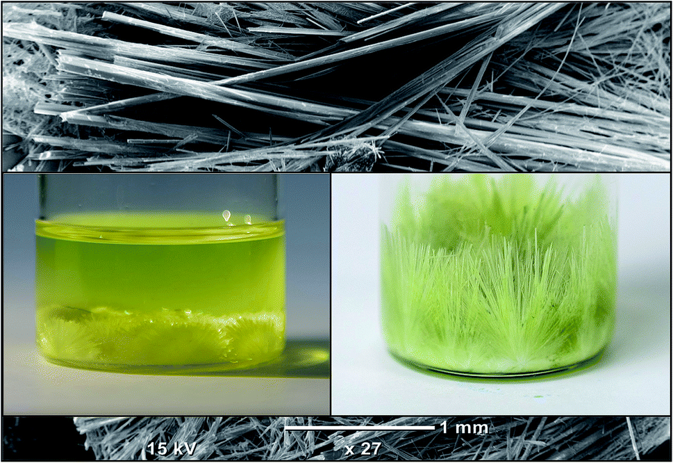 | ||
| Fig. 1 SEM image and photos of the PbI2 crystals grown in the DMF solution. | ||
The surface morphology of the one-dimensional micro rods was investigated using JEOL 7600 scanning electron microscope while the thermal stability of the prepared micro-rods was studied by thermogravimetric analysis (TGA) and differential scanning calorimetry (DSC). TGA and DSC analyses were undertaken by PerkinElmer TGA 4000 Analyzer and PerkinElmer DSC 8500 instruments under nitrogen environment, respectively. The Raman spectra were obtained by using Jobin-Yvon HR800 UV-Vis-NIR, Raman spectrometer equipped with an Olympus BX 40 attachment. The excitation wavelength was 514.5 nm with an energy setting of 1.2 mW were employed from a coherent argon-ion laser (Innova, model 308). The Raman spectra were recorded by means of back scattering geometry with an acquisition time of 50 seconds. Fourier transform infrared spectroscopy was performed using, PerkinElmer (Spectrum 2000, USA) over the wave number range 4000–400 cm−1. X-ray diffraction (XRD) patterns were recorded using EMPYREAN diffractometer operated at 45 kV, 40 mA with Kα1 and Kα2 radiations having 1.540598 Å and 1.544426 Å wavelength, respectively, with a scan speed of 1 s per step and a step size of 0.013° 2θ.
3 Results and discussion
Fig. 2(a–f) shows the morphology of the prepared microcrystalline rods at different magnification. The morphological examination of Fig. 2(a and d) indicates that the micro crystals grow in longitudinal dimension having lengths up to 5 mm. Furthermore, it can also be seen that the lateral dimensions of the microcrystals are of 10–100 μm diameter. The SEM images also reveal that the microcrystals of PbI2 (Fig. 2(b and c)) and MAPbI3 (Fig. 2(e and f)) contain pores having a size in the submicron range. The higher magnification image of the microcrystal show that many parallel nanowires are joined longitudinally to form a large micro-rod. Due to slight differences in the dimensions of the nanowires, they've left a small space between adjacent wires while joining together which results in the formation of hallow regions. However, no adjacent cracks have also been observed on the microcrystalline rods at lower magnification which can be regarded as there is no visual defect during the joining of two or more crystalline wires.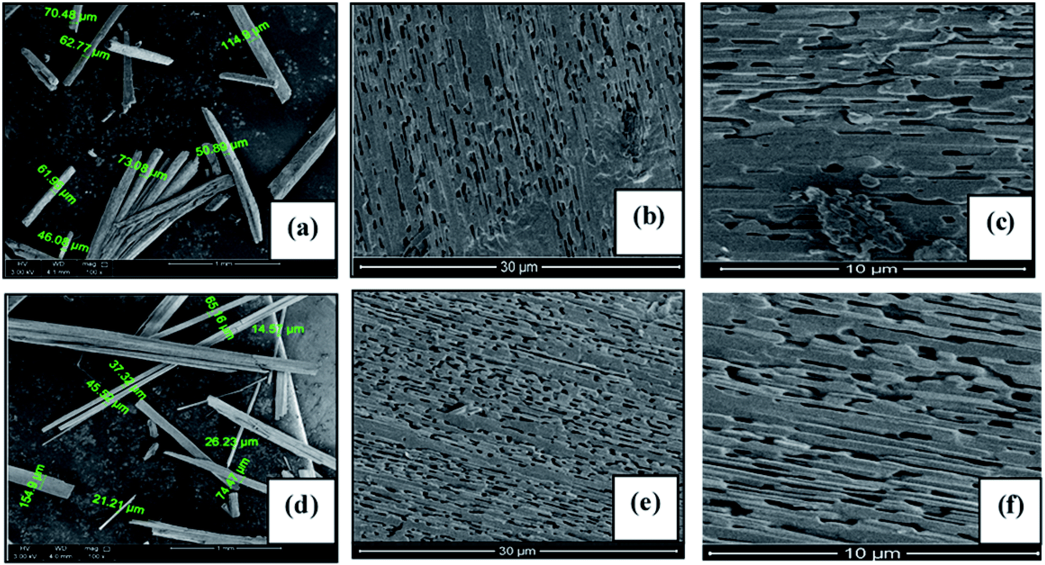 | ||
| Fig. 2 FESEM images of the PbI2 and MAPbI3 the micro-rods taken at different magnification. (a–c) represents the PbI2 while the (d–f) denotes the MAPbI3. | ||
The compositional analysis of the developed microcrystals has been performed using EDS and the results are shown in Fig. 3(a and b). For all crystals the EDS spectra show well defined peaks corresponding to elements such as carbon lead and iodine. There are two feature peaks at 2.32 and 10.5 keV corresponding to the lead and two feature peaks at 3.98 and 4.2 keV which can be assigned to iodine elements in PbI2 crystals. In the case of PbI2, the atomic composition of the microcrystals indicates the presence of Pb with I in a 1:2.1 ratio, which is in close agreement with the PbI2, confirming the formation of pure phases. However, in the case of MAPbI3, this ratio is turned to 1:1.5. This might be due to the existence of separate phases of PbI2 and MAI. Here it is also important to note that the MAPbI3 has been extremely sensitive to high energy electron beam radiation and thus it is easy to decompose into PbI2 during EDS measurement.7
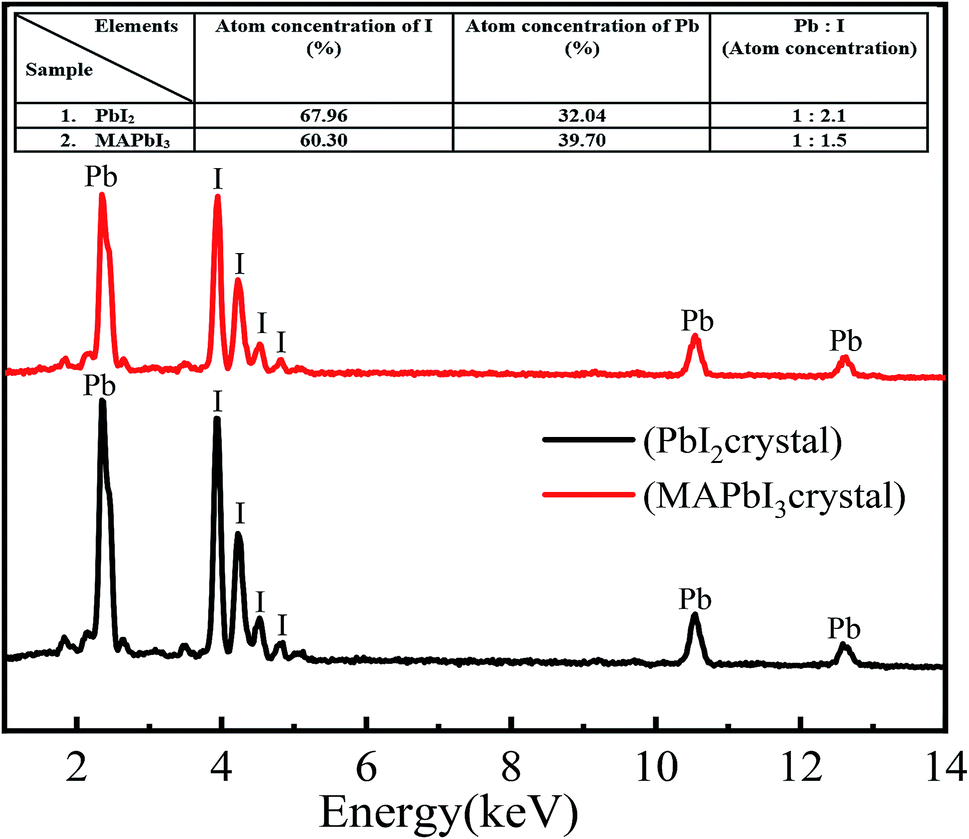 | ||
| Fig. 3 EDS spectra of the micro-rods: PbI2 and MAPbI3. | ||
In order to have more insight of the developed microcrystals of PbI2 and MAPbI3, HRTEM analysis was conducted and the results are presented in Fig. 4(a and b). TEM images taken from the selected region to show the further existence of the nano-pores in the micro-rods and no cracks are observed in a microcrystal surface. Further high-resolution TEM images of PbI2 MAPbI3 crystals cannot be obtained because the PbI2 and MAPbI3 crystals are sensitive to high-energy electron beam irradiation, which can cause distortion of their crystal structure.
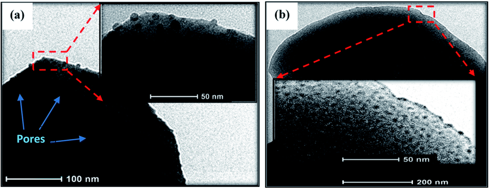 | ||
| Fig. 4 TEM images for crystal rods PbI2 (a), MAPbI3 (b), insets shows higher magnification images of same surface. | ||
X-ray diffraction spectra of synthesized one-dimensional crystals are shown in Fig. 5. For a clear comparison, the XRD spectra of the starting materials in powder form, commercially purchased from Sigma-Aldrich, is also included as shown in Fig. 5(a and b). Fig. 5(a) corresponds to the XRD spectrum of the PbI2 crystal (yellow circles) and commercially purchased PbI2 powder (black lines). Both XRD patterns showed a hexagonal system (Pm1(164) space group) with a = b = 0.4557 nm and c = 0.6979 of PbI2 and 2H polytype structure (hematite, JCPDS file no. 07-0235).8 The most intense diffraction peak is obtained at 12.60° that corresponds to the (001) lattice plane. However, the peak intensity at this angle for PbI2 crystal is much higher than the PbI2 powder. Other prominent peaks are observed at 25.5°, 25.93°, 34.2°, 38.67° and 52.3° corresponding to the (002), (011), (102), (003), and (004) lattice planes of PbI2. Some other preferential orientation peaks of PbI2 corresponding to (113), and (114) planes are observed at higher diffraction angles 56.4° and 67.5°, respectively as indicated in the Fig. 5(a). The crystalline orientations obtained in the present work are different from those of previous literatures for MAPbI3 films as well as bulk crystals.9,10 In the prepared crystals, the d-spacing is fingerprints of specific sample that is determined by XRD. It can be noticed that the d-spacing of the PbI2 crystal is more as compared to PbI2 powder resulting in shifting of the lattice planes towards lower angles. The shifting of plane spacing (d-value) may be due to rearrangement of lattice positions.11
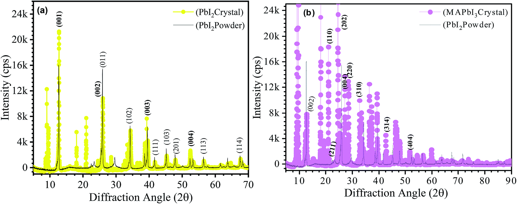 | ||
| Fig. 5 Diffraction patterns of PbI2 powder, PbI2 crystals and MAPbI3 micro crystalline rods recorded at room temperature. (a) PbI2 crystal (yellow data points) and PbI2 powder (black line). (b) MAPbI3 crystal (magenta data points) and PbI2 powder (black line). | ||
Similarly, the MAPbI3 one dimensional crystals have adopted the hexagonal structure with Pm1(164) space group. High intensity diffraction peaks are obtained at lower angle positions 9.0°, 9.5°, 18.1° and 24.5° (Fig. 5(b)) overwhelmingly dominate the diffraction pattern. The high intensity diffraction peaks confirm the high crystalline nature of the prepared phase. The same c-axis diffraction peaks obtained in PbI2 powder at (002), (003), and (004) are also obtained in MAPbI3 crystals at angles 12.67°, 19.05°, and 25.5° respectively with very poor intensities. Intense diffraction peaks respectively assigned to (110), (202), (004) and (220) confirms the MAPbI3 phase. Furthermore few low intensity marker of MAPbI3 phase is also present at (310), (314), and (404).12 The unidentified peaks representing stable phase at the room temperature did not match either the pure PbI2 or MAI phase. This suggests a new intermediate phase, which might be a complex of PbI2–DMF or complex of PbI2–MAI–DMF.13
The structure of the synthesized one-dimensional microcrystals has also been examined by the FTIR and the results are shown in Fig. 6. The FTIR vibrations at 660 and 860 cm−1 show the features characteristic of C–O stretching and C–N stretching. The absorption peak at 840 cm−1 produced by e bending vibration peak of CH3. Peaks at 1007, 1058 cm−1 belongs to sp3 C–H stretching. Signal around 2900 cm−1, that is a strong marker of the presence of this group are week here, but they are very prominent in RAMAN. Peaks between 1250–1550 cm−1 of the frequency of vibration belongs to C–H and N–H bending. However, overshoots at 1265 and 1385 cm−1 is not visible in MAPbI3. The stretching vibration due to C![[double bond, length as m-dash]](https://www.rsc.org/images/entities/char_e001.gif) O bond appeared at 1620 cm−1 and at 1660 cm−1 (this group is present in the DMF molecule as well). However, the CO bond strength decreased with the MAI addition in PbI2. It has been observed that there are no O–H stretching vibrations around 3500 cm−1 suggesting absence of hydrated or adsorbed water.14,15 The O–H oscillations of water molecules are embedded in such a way that they affect the hydrogen bonds between the N–H group and the iodide because the N–H stretch vibrations are known for their sensitivity to the strength of the interaction between the methylammonium and the iodide. Even though, the MAI is not present in the solutions except MAPbI3 but C–H and N–H stretching and bending vibrations are very similar for all the dry crystals. The FTIR peaks in the 500–1700 cm−1 range are well correspond to the Raman features as shown in Fig. 7. Though, some peaks cannot be found in the infrared spectra, but are present in the Raman spectra precisely above 1700 cm−1. This is because of the fact that the vibrational energy in Raman is active due to changes in polarization whereas IR active intensities are depending on the dipole moment.16,17
O bond appeared at 1620 cm−1 and at 1660 cm−1 (this group is present in the DMF molecule as well). However, the CO bond strength decreased with the MAI addition in PbI2. It has been observed that there are no O–H stretching vibrations around 3500 cm−1 suggesting absence of hydrated or adsorbed water.14,15 The O–H oscillations of water molecules are embedded in such a way that they affect the hydrogen bonds between the N–H group and the iodide because the N–H stretch vibrations are known for their sensitivity to the strength of the interaction between the methylammonium and the iodide. Even though, the MAI is not present in the solutions except MAPbI3 but C–H and N–H stretching and bending vibrations are very similar for all the dry crystals. The FTIR peaks in the 500–1700 cm−1 range are well correspond to the Raman features as shown in Fig. 7. Though, some peaks cannot be found in the infrared spectra, but are present in the Raman spectra precisely above 1700 cm−1. This is because of the fact that the vibrational energy in Raman is active due to changes in polarization whereas IR active intensities are depending on the dipole moment.16,17
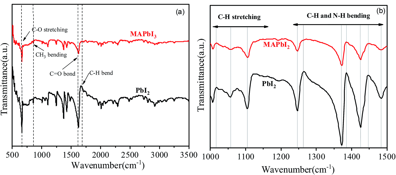 | ||
| Fig. 6 FTIR spectra of PbI2 and MAPbI3 micro-rods: (a) 500–3500 cm−1 and (b) 1100–1500 cm−1. | ||
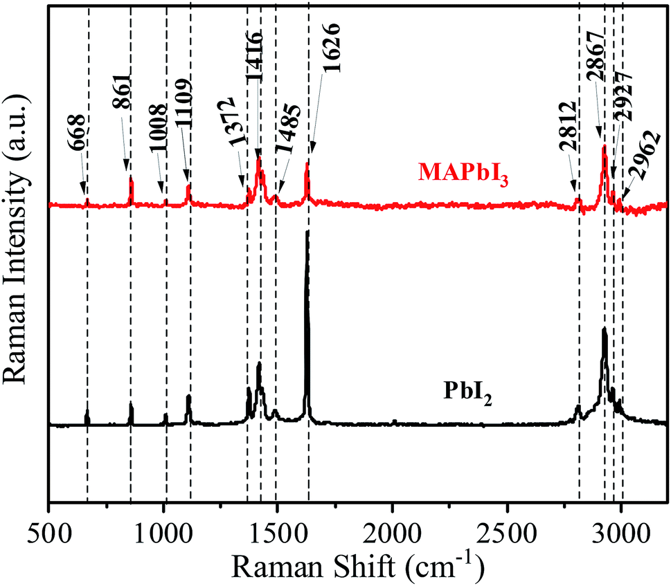 | ||
| Fig. 7 Raman spectra of PbI2, and MAPbI3 one dimensional micro-rods. | ||
Raman spectroscopic analysis of the prepared materials is presented in Fig. 7. Characteristic internal vibrations appear at three energetic regions; (i) the C–N stretching at 600–1100 cm−1, (ii) CH3 and NH3 bending around 1300–1600 cm−1 and (iii) CH3 and NH3 is stretching at around 3000 cm−1. Qualitatively, each PbI2, and MAPbI3 shows similar vibrational properties with three energetic regions, hence there is no phase transformation/change during the crystallization process. These ranges are consistent with previous reports.18–20
Thermogravimetric analysis (TGA) is used to determine the thermal stability of the micro-rods and the results are presented in Fig. 8. It can be noticed that weight loss is observed in two temperature ranges; (i) between 110–116 °C showing weight loss less than 15% for all samples. Minimum (12%) mass loss is obtained in PbI2 crystal at 110.83 °C and maximum (15%) is in MAPbI3 micro-rods at 115.87 °C. The TGA weight loss profile implies that these materials have not undergone thermal decomposition or sublimation during 1st stage and mass loss is solely due to the removal of absorbed moisture from the microcrystals. Because sublimation has been defined as the point where at least 20% of mass loss of the sample has happened.21 The 2nd weight loss is observed between 550 °C and 600 °C for the synthesized crystals. This sequential decomposition is observed in the perovskite materials where organic component decomposes by the subsequent mass loss of HI and CH3NH2 because the latter species is more tightly incorporated in the perovskite matrix. Sequential decomposition pathway occurs only when the organic species are combined into the perovskite structure. This type of decomposition is not observed in the pure PbI2 and MAI powder. PbI2 powder (99% pure) undergoes 90% weight loss at 646 °C and MAI undergoes 100% weight loss at 185 °C (ref. 22) which means pure organic material and inorganic material shows single step mass loss decomposition behavior. This single step loss is not observed in the TGA of all the crystal samples. Thermal behavior of prepared microcrystals is in a good agreement with the previous results.22,23 DSC was also used to effectively detect phase transitions and to gain further insight into the thermal behavior of the microcrystals. The heating–cooling cycle DSC measurements over the temperature range of 50–200 °C has been carried out and corresponding results are shown in the inset of Fig. 8. A narrow endothermic peaks in a temperature range of 125–132 °C is noticed which can be ascribed to the polymorphic transformation while heating.24
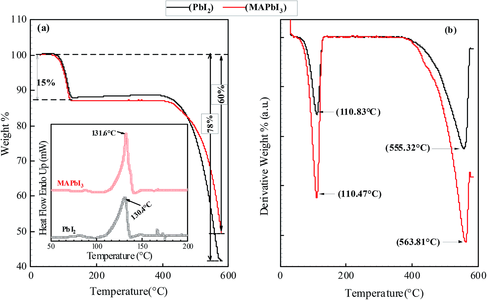 | ||
| Fig. 8 TGA heating curves of individual crystals expressed as (a) weight% and its (b) derivatives as a function of applied temperature. Inset shows the DSC heating curves for the PbI2 and MAPbI3 micro-rods. | ||
4 Conclusions
In summary, facial growth of one-dimensional PbI2 and MAIPbI3 based perovskite micro rods has been undertaken. The morphological, structural and thermal properties of the one-dimensional perovskite micro-rods have been examined using various characterization techniques. X-ray diffraction and SEM/EDX analyses confirm phase purity and high crystallinity of the developed micro-rods. Thermal analysis (TGA) indicates decent thermal stability of PbI2 and MAIPbI3 microcrystals. The decomposition of PbI2 microcrystals observed in the temperature of 500–600 °C is in good agreement with the thermal decomposition of the one-dimensional perovskites. FTIR and Raman spectroscopy analyses confirm the existence of strong interactions between different stable groups in the crystals. The morphological studies (SEM/TEM) confirm crack free morphology of PbI2 and MAPbI3 micro-rods with porous structure. The micro-rods of PbI2 and MAPbI3 may be considered for the application in perovskites photovoltaics and beyond. Hence, the development of these unique one-dimensional micro-rods represents a novel concept in materials design and synthesis that may foster ground-breaking research.Conflicts of interest
The authors declare that there is no conflict of interest.Acknowledgements
This work is supported by Qatar University Internal Grant No. QUCG-CAM-2018/19-1. The findings achieved herein are solely the responsibility of the authors. The authors also acknowledge the Qatar National Library for providing the financial support to pay open access charges for this publication.References
- S. Tongay, Preface to a Special Topic: 2D Materials and Applications, Appl. Phys. Rev., 2018, 5(1), 010401 Search PubMed
.
- G. R. Bhimanapati, et al., Recent Advances in Two-Dimensional Materials beyond Graphene, ACS Nano, 2015, 9(12), 11509–11539 CrossRef CAS PubMed
- V. Kaushik, et al., Scalable Exfoliation of Bulk MoS(2) to Single- and Few-Layers Using Toroidal Taylor Vortices, Nanomaterials, 2018, 8(8), 587 CrossRef
- L. Yang, et al., Properties, Preparation and Applications of Low Dimensional Transition Metal Dichalcogenides, Nanomaterials, 2018, 8(7), 463 CrossRef
- J. Huang, Y. Shao and Q. Dong, Organometal Trihalide Perovskite Single Crystals: A Next Wave of Materials for 25% Efficiency Photovoltaics and Applications Beyond?, J. Phys. Chem. Lett., 2015, 6(16), 3218–3227 CrossRef CAS
- P.-A. Mante, et al., Electron–acoustic phonon coupling in single crystal CH3NH3PbI3 perovskites revealed by coherent acoustic phonons, Nat. Commun., 2017, 8, 14398 CrossRef CAS PubMed
- S. Chen, et al., Atomic scale insights into structure instability and decomposition pathway of methylammonium lead iodide perovskite, Nat. Commun., 2018, 9(1), 4807 CrossRef PubMed
- P. E. Tomaszewski, Structural phase transitions in crystals. I. Database, Phase Transitions, 1992, 38(3), 127–220 CrossRef CAS
- Y. Fu, et al., Solution growth of single crystal methylammonium lead halide perovskite nanostructures for optoelectronic and photovoltaic applications, J. Am. Chem. Soc., 2015, 137(17), 5810–5818 CrossRef CAS PubMed
- M. Xiao, et al., A fast deposition-crystallization procedure for highly efficient lead iodide perovskite thin-film solar cells, Angew. Chem., Int. Ed. Engl., 2014, 53(37), 9898–9903 CrossRef CAS
- P. Beckmann, ChemInform Abstract: A Review of Polytypism in Lead Iodide, Cryst. Res. Technol., 2010, 45, 455–460 CrossRef CAS
- T. Baikie, et al., Synthesis and crystal chemistry of the hybrid perovskite (CH3NH3)PbI3 for solid-state sensitised solar cell applications, J. Mater. Chem. A, 2013, 1(18), 5628–5641 RSC
- B. R. Vincent, et al., Alkylammonium lead halides. Part 1. Isolated PbI64−ions in (CH3NH3)4PbI6·2H2O, Can. J. Chem., 1987, 65(5), 1042–1046 CrossRef CAS
- J. Idígoras, et al., The interaction between hybrid organic–inorganic halide perovskite and selective contacts in perovskite solar cells: an infrared spectroscopy study, Phys. Chem. Chem. Phys., 2016, 18(19), 13583–13590 RSC
- M. A. Pérez-Osorio, et al., Vibrational Properties of the Organic–Inorganic Halide Perovskite CH3NH3PbI3 from Theory and Experiment: Factor Group Analysis, First-Principles Calculations, and Low-Temperature Infrared Spectra, J. Phys. Chem. C, 2015, 119(46), 25703–25718 CrossRef
- N. Ahn, et al., Highly Reproducible Perovskite Solar Cells with Average Efficiency of 18.3% and Best Efficiency of 19.7% Fabricated via Lewis Base Adduct of Lead(II) Iodide, J. Am. Chem. Soc., 2015, 137(27), 8696–8699 CrossRef CAS PubMed
- E. Mosconi, et al., Structural and electronic properties of organo-halide lead perovskites: a combined IR-spectroscopy and ab initio molecular dynamics investigation, Phys. Chem. Chem. Phys., 2014, 16(30), 16137–16144 RSC
- M. Ledinský, et al., Raman Spectroscopy of Organic–Inorganic Halide Perovskites, J. Phys. Chem. Lett., 2015, 6(3), 401–406 CrossRef
- R. G. Niemann, et al., Halogen Effects on Ordering and Bonding of CH3NH3+ in CH3NH3PbX3 (X = Cl, Br, I) Hybrid Perovskites: A Vibrational Spectroscopic Study, J. Phys. Chem. C, 2016, 120(5), 2509–2519 CrossRef CAS
- C. Quarti, et al., The Raman Spectrum of the CH3NH3PbI3 Hybrid Perovskite: Interplay of Theory and Experiment, J. Phys. Chem. Lett., 2014, 5(2), 279–284 CrossRef CAS
- B. D. Fahlman and A. R. Barron, Substituent effects on the volatility of metal β-diketonates, Adv. Mater. Opt. Electron., 2000, 10(3-5), 223–232 CrossRef CAS
- A. Dualeh, et al., Thermal Behavior of Methylammonium Lead-Trihalide Perovskite Photovoltaic Light Harvesters, Chem. Mater., 2014, 26(21), 6160–6164 CrossRef CAS
- Y. Liu, et al., Two-Inch-Sized Perovskite CH3NH3PbX3 (X = Cl, Br, I) Crystals: Growth and Characterization, Adv. Mater., 2015, 27(35), 5176–5183 CrossRef CAS
- T. Supasai, et al., Formation of a passivating CH3NH3PbI3/PbI2 interface during moderate heating of CH3NH3PbI3 layers, Appl. Phys. Lett., 2013, 103(18), 183906 CrossRef
| This journal is © The Royal Society of Chemistry 2019 |