 Open Access Article
Controllable etching-induced contact enhancement for high-performance carbon nanotube thin-film transistors†
Zhengxia Lv adef,
Dan Liua,
Xiaoqin Yub,
Qianjin Lvc,
Bing Gaob,
Hehua Jin
 *a,
Song Qiu
 *a,
Chuanling Menc,
Qijun Song
 b and
Qingwen Li*ad
aKey Laboratory of Multifuctional Nanomaterials and System Integration, Suzhou Institute of Nano-Tech and Nano-Bionics, Chinese Academy of Science, Suzhou, 215123, P. R. China. E-mail: hhjin2008@sinano.ac.cn; sqiu2010@sinano.ac.cn; qwli2007@sinano.ac.cn
bCollege of Chemical and Material Engineering, Jiangnan University, Wuxi 214122, P. R. China
cSchool of Energy and Power Engineering, University of Shanghai for Science and Technology, 516 Jungong Road, Shanghai 200093, P. R. China
dSchool of Physical Science and Technology, ShanghaiTech University, Shanghai 200120, P. R. China
eUniversity of Chinese Academy of Sciences, Beijing 100049, P. R. China
fShanghai Institute of Ceramics, University of Chinese Academy of Sciences, 1295 Dingxi Road, Shanghai 200050, P. R. China
First published on 4th April 2019
Abstract
Semiconducting single-walled carbon nanotubes (s-SWNTs) show great promises in advanced electronics. However, contact resistance between the nanotubes and metal electrode has long been a bottleneck to the development of s-SWNTs in high-performance electronic devices. Here we demonstrate a simple and controllable strategy for enhancing the electrode contact and therefore the performance of s-SWNT thin film transistors by plasma etching treatment, which effectively removes the polymer residues, including the photoresist and the conjugated molecules, adsorbed on the surface of s-SWNTs. As a result, the contact resistance is reduced by 3 times and the carrier mobility rises by up to 70%. Our method is compatible with current silicon semiconductor processing technology, making it a viable effective approach to large-scale application of s-SWNTs in the electronics industry.
Introduction
Semiconducting single-walled carbon nanotubes (s-SWNTs) have drawn increasing interest in the development of flexible and transparent electronic devices due to their unique one-dimensional structure, tuneable bandgap and excellent electronic properties.1–3 Recently, great progress in selectively sorting s-SWNTs with purity higher than 99.9%4,5 has enabled the fabrication of s-SWNT based field effect transistors (FETs) with high carrier mobility, high on/off ratio, low off-state current and steep sub-threshold swing. These FETs are desirable for developing complementary metal-oxide-semiconductor (CMOS) electronics with low dynamic and static power consumption. Meanwhile, s-SWNT network-based thin-film transistors (TFTs) have also been extensively investigated and many potential applications have been demonstrated, including infrared detection,6,7 flexible displays,8,9 radio frequency devices,10,11 integrated circuits12,13 and other functional devices.14,15 However, despite significant improvements to the subthreshold swing and on/off ratio of s-SWNT thin film devices through various optimised techniques, the low and uncontrollable carrier mobility and current density are still major hurdles to achieving practical utility.Establishing ohmic contact between the s-SWNTs and the metal electrode is crucial to fabricate high-performance transistors. For a s-SWNT TFT device, the total resistance is composed of channel and contact resistance. The channel resistance tends to vary inversely with the channel length of TFTs. When the channel length is reduced to microscale or nanoscale, the channel resistance becomes a negligible component of the total resistance relative to the contact resistance. The latter, therefore, tends to be the main hurdle to improving the performance of s-SWNT TFTs. Furthermore, the contact interfaces between the s-SWNTs and the metal electrodes directly determine the injection efficiency of carriers. Therefore, three main approaches have been developed to solve contact-related problems, including the removal of dispersant organic molecules on the sorted s-SWNTs,16–18 the use of electrode metals with a relatively low work function to improve transport at the interfaces19 and the formation of chemical bonds between SWNTs and electrode.20,21 However, dispersant removal may lead to the aggregation of carbon nanotubes (CNTs), which is hard to produce uniform films in large-area. Deposited metal electrodes with low work function are not stable in the air, resulting in unstable and uncontrollable performance of the devices. Formation of chemical bond between SWNT and electrode is often complex and difficult to control. For these reasons, it is necessary to develop a simple and effective method for the fabrication of controllable s-SWNT TFTs with high performance.
Here, we demonstrate a simple and controllable method to fabricate high-performance s-SWNT TFTs, which is compatible with current silicon semiconductor processing technology. Through simply introducing a plasma etching procedure into the normal photolithography process, the performance of the s-SWNT TFTs is greatly improved. In our modified procedures, the contact resistance decreases more than threefold and the average carrier mobility reaches up to 91 cm2 V−1 s−1, which is in the highest level compared with previously reported results. After thoroughly investigating the influence of etching time on the performance of s-SWNT TFT devices, we concluded that the removal of impurity and the structural damage of s-SWNT upon plasma etching may play a key role in enhancing and stabilizing not only the contact between s-SWNT films and metal electrodes, and thus promote the performance of s-SWNT TFTs.
Results and discussion
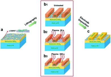
To prepare s-SWNT dispersion with high purity, conjugated polymer-assisted separation method was chosen, using poly[9-(1-octylonoyl)-9H-carbazole-2,7-diyl] (PCz) as dispersant, as reported in our previous studies.5,16 Arc-discharged SWNTs were employed because they have proper diameters and bandgap distribution. After typical procedure of sonication followed by two rounds of centrifugation, the dispersion was collected for further analyses and applications. The detailed process and purity evaluation in terms of the Φ value22 are shown in ESI 1.†Fig. 1 shows the modified fabrication process for high-performance s-SWNT TFTs. The TFTs were fabricated with channel length of 2 μm and channel width of 10 μm. Firstly, s-SWNT networks were fabricated on the SiO2/Si substrate by dip-coating and the photoresist was spin-coated on the surface of the s-SWNTs/SiO2/Si under condition of yellow light. Then, the source and drain electrodes of the transistors were patterned by lithography. Next, the exposed electrode pattern areas were treated by plasma etching, a procedure with an important influence on device performance. In this procedure, the power was set at 100 W and oxygen flow was 100 sccm. Different etching times ranging from 10 s to 300 s were performed. Finally, Pd (30 nm) was deposited as the electrode through thermal evaporation followed by lift-off. The s-SWNT TFTs fabricated with and without plasma etching were investigated in detail.
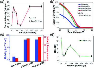
The performances of the as-fabricated s-SWNT TFTs are shown in Fig. 2. To evaluate the reliability of the etching procedure, the statistical current densities of the TFTs etched for different times were calculated, as shown in Fig. 2a. Two peak current distributions can be observed. When the etching time was increased from 0 to 90 s, the peak current appeared at around 20 s, indicating that relatively brief etching markedly enhanced the device performance compared with no treatment or slightly longer etching times. Interestingly, however, the absolute maximum current was recorded when the treatment time exceeded 180 s and remained relatively stable when the etching time was prolonged to 300 s. The on-current increased from 130 μA (untreated) to 240 μA after 300 s plasma etching. Fig. 2b shows the characteristic linear transfer curves of s-SWNT TFTs with selected plasma etching times of 0 s, 20 s, 180 s and 300 s. The transfer curves for all of the plasma etching times are shown in Fig. S4.† The shapes of the transfer curves indicate that the s-SWNT TFTs display p-type carrier transports. As mentioned above, for all plasma etching times equal to or greater than 180 s, the s-SWNT TFT devices exhibit almost identical, greatly enhanced performance. Besides the obvious increase of current density, the threshold voltages were also decreased. Fig. 2c exhibits the average carrier mobilities and the average current densities of the fabricated TFTs with plasma etching times of 0 s, 180 s and 300 s. Under 180 s treatment, the on-current density was increased to 24 μA μm−1 and the mobility of the device was increased from 56 cm2 V−1 s−1 to 91 cm2 V−1 s−1. Fig. S7† shows the logarithmic transfer curves of s-SWNT TFTs with different etching times, which are consistent with Fig. 2a, indicating the stable and reliable performance of the as-fabricated TFTs.
Fig. 2d shows the relationship between average contact resistance and plasma etching time. To evaluate the change of contact resistance (2Rc) between s-SWNTs and metal electrode, the Y function was calculated.23,24 The detailed calculation process is shown in ESI 2.† The contact resistance decreased from 14.46 kΩ for the untreated sample to 3.36 kΩ for the sample with the longest etching time of 300 s. The variation of 2Rc with etching time was consistent with the response of the current density shown in Fig. 2a, indicating enhancement of the performance substantially caused by better contact between s-SWNT and metal electrode after plasma treatment. The performances of s-SWNT transistors reported in recent papers were compared with ours in this work. Fig. S6† presents the statistics for on/off ratio and carrier mobility of the s-SWNT TFTs.25–37 For the random s-SWNT film-based TFTs fabricated in our work, merely by plasma treatment, the devices were able to markedly outperform the previously reported random film-based devices, and were even comparable with devices fabricated using aligned s-SWNT films.
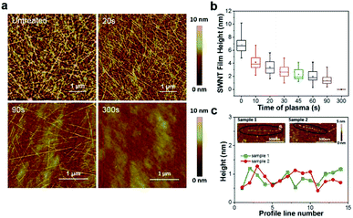
To understand the role of plasma etching in the performance enhancement of the s-SWNT TFT devices, we first characterised the s-SWNT films by atomic force microscopy (AFM) and scanning electron microscopy (SEM) under different etching times. As shown in Fig. 3a and S8,† the AFM image for the untreated s-SWNT film exhibits numerous bright spots, suggesting residual impurities on the surface of s-SWNT film, which may be ascribed to the small amounts of photoresist and conjugated polymers wrapped on s-SWNTs. The height of the untreated s-SWNTs was about 6–8 nm, which were consisted of 2–3 layers of s-SWNTs. For the s-SWNT film treated with 20 s plasma etching, the surface of s-SWNTs became clean, and the height decreased to 3–5 nm, which indicates the removal of organic impurities and may be accompanied by the slightly destroy of s-SWNT. As the etching time increased, the s-SWNTs were progressively destroyed. When the etching time was prolonged to 90 s, the height of the s-SWNT films was lower than 2.0 nm, suggesting that the top 1–2 layers of s-SWNTs had already been etched, and only the bottom layer of s-SWNTs left, which formed a sparse network. Similarly, after 90 s etching, no s-SWNTs were observed in the SEM image, and the height of a single s-SWNT was measured, ranging from 0.49 to 1.47 nm as shown in Fig. 3c. Considering that previous research of SWNT etching process determined the height of PCz-wrapped s-SWNT is about 1.5–2.0 nm, it can be inferred that the remaining s-SWNTs were broken into tubular fragments. When the etching time increased to 180 s, no remaining s-SWNTs could be seen in the AFM and SEM images, meaning that most of the s-SWNTs had been greatly etched. In addition, as shown in Fig. 3b, the height of the overall s-SWNT film was also found to gradually decrease with the increase of etching time, further demonstrating the destruction of the s-SWNTs.
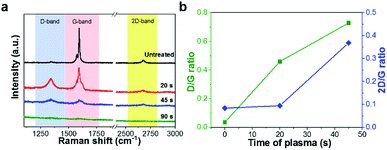
Further evidence of structural damage by plasma etching was provided by the Raman, XPS and absorption spectra. Fig. 4a shows the Raman spectrum of s-SWNT film excited by a 633 nm laser. Typically, s-SWNTs have two typical peaks, corresponding to the D and G band. The D band peak is usually located at 1300 cm−1 and originates from structural defects. The G band peak is generally located at 1590 cm−1 and stems from planar vibrations of carbon atoms in SWNTs. When the etching time was less than 20 s, the G band peak is obvious and strong, indicating that most of the s-SWNTs remained intact. However, with prolonged etching time, the intensity of the D band peak gradually increased, suggesting increased structural defects of the s-SWNTs introduced by plasma etching treatment. After the etching time reached to 45 s, the intensity of the G band peak decreased to that of the D band peak and became very weak. When the etching time was extended to 90 s, the Raman signals almost disappeared, suggesting that the density of remaining s-SWNTs was very low. In contrast, as shown in Fig. S9,† a 2D band peak at 2650 cm−1 arose with the increase of etching time, indicating the generation of a planar sp2 structure, which may origins from SWNTs with a high density of defects. Fig. 4b exhibits the D/G and 2D/G ratios at different plasma treatment times, which are in good agreement with the structural observations from AFM and SEM. The increase of these ratios indicates that defects and a planar sp2 fragments increased with prolonged plasma treatment time. Because the PCz and s-SWNTs both have their own characteristic absorption peaks, absorption spectroscopy can be used to track their changing contents. To obtain the absorption spectra, the s-SWNT film was deposited on a transparent quartz substrate and then etched for different times. As shown in Fig. S10,† the absorption peaks of s-SWNTs and PCz gradually disappear with the increase of etching time, which again demonstrates that the plasma etching treatment not only degrades the conjugated polymer but also destroys the structure of the s-SWNTs.
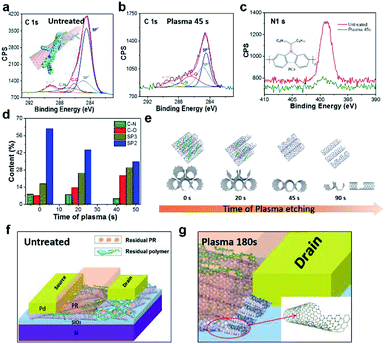
To further understand the degradation of polymer and the structural variation of SWNTs during plasma treatment, the XPS spectrum of the s-SWNT film was used to evaluate the contents of carbon and nitrogen, as shown in Fig. 5. (The XPS spectra for all of the plasma etching times are shown in Fig. S11.†) The C 1s peak can be deconvoluted into five peaks,38,39 i.e. π–π* (289.2 eV), C–N (287 eV), C–O (286.1 eV), C![[double bond, length as m-dash]](https://www.rsc.org/images/entities/char_e001.gif) C (284.9 eV) and C–C (284.5 eV). As shown in Fig. 5a and b, the C 1s peak of untreated and etched for 45 s samples explained intensity of the peak decreased and the sp2 structure transformed to sp3 structure with the increase of plasma treatment time, indicating the decreased content of s-SWNTs and edge defect introduced by plasma treatment, which is consistent with the above analyses. As shown in Fig. 5c, the intensity of N 1s was greatly reduced after 45 s treatment, further demonstrating the rapid degradation of PCz. Fig. 5d shows the contents of four chemical bond types after etching times ranging from 0 to 45 s. The decreasing content of C–N groups demonstrates the degradation of PCz, as nitrogen only existing in PCz, while the increasing content of C–O groups implies the introduction of more defects into the s-SWNTs. Moreover, the increasing content of C–C groups and decreasing content of C
C (284.9 eV) and C–C (284.5 eV). As shown in Fig. 5a and b, the C 1s peak of untreated and etched for 45 s samples explained intensity of the peak decreased and the sp2 structure transformed to sp3 structure with the increase of plasma treatment time, indicating the decreased content of s-SWNTs and edge defect introduced by plasma treatment, which is consistent with the above analyses. As shown in Fig. 5c, the intensity of N 1s was greatly reduced after 45 s treatment, further demonstrating the rapid degradation of PCz. Fig. 5d shows the contents of four chemical bond types after etching times ranging from 0 to 45 s. The decreasing content of C–N groups demonstrates the degradation of PCz, as nitrogen only existing in PCz, while the increasing content of C–O groups implies the introduction of more defects into the s-SWNTs. Moreover, the increasing content of C–C groups and decreasing content of C![[double bond, length as m-dash]](https://www.rsc.org/images/entities/char_e001.gif) C groups may be ascribed to destruction of SWNTs during plasma treatment, revealing that sp2 carbon was gradually converted into sp3 carbon. We illustrated the structural change of the s-SWNT film under plasma etching in Fig. 5e, which can be seen to proceed through several stages. The initial s-SWNTs are wrapped by PCz and a small amount of photoresist. In the first stage, the residual PCz and photoresist on the s-SWNTs are degraded. In the second stage, the s-SWNTs on the top layer are gradually destroyed and transformed into planar fragments of sp2 structure. In the third stage, the s-SWNTs on the top layer are almost completely removed while the exposed bottom s-SWNTs still maintain their integrity. In the fourth stage, the bottom s-SWNTs are also transformed into planar fragments after greatly destroyed. Finally, most of the s-SWNTs are greatly etched while the s-SWNTs near the edge of the photoresist are continuously exposed and converted into planar fragments.
C groups may be ascribed to destruction of SWNTs during plasma treatment, revealing that sp2 carbon was gradually converted into sp3 carbon. We illustrated the structural change of the s-SWNT film under plasma etching in Fig. 5e, which can be seen to proceed through several stages. The initial s-SWNTs are wrapped by PCz and a small amount of photoresist. In the first stage, the residual PCz and photoresist on the s-SWNTs are degraded. In the second stage, the s-SWNTs on the top layer are gradually destroyed and transformed into planar fragments of sp2 structure. In the third stage, the s-SWNTs on the top layer are almost completely removed while the exposed bottom s-SWNTs still maintain their integrity. In the fourth stage, the bottom s-SWNTs are also transformed into planar fragments after greatly destroyed. Finally, most of the s-SWNTs are greatly etched while the s-SWNTs near the edge of the photoresist are continuously exposed and converted into planar fragments.
Based on the above analyses, a possible mechanism is proposed for the performance enhancement by plasma etching. Here, graphene-like fragments were envisaged to explain the enhanced contact between electrode and s-SWNTs according to the results discussed above. When photoresist is used, the photoresist is etched faster than the s-SWNTs.40 After photolithography, the residual photoresist and conjugated polymers adsorbed on the surface of s-SWNTs strongly impede the contact between s-SWNTs and metal electrode, and therefore reduce the injection efficiency of the carriers (as shown in Fig. 5e–f and S12†). Under a short etching time of less than 20 s, the photoresists and conjugated polymers on the s-SWNTs are degraded by oxygen etching. When further increasing the etching time to 20 s, the s-SWNTs on the top layer are gradually thinned and converted into broken tubular or graphene-like fragments, resulting in better contact between s-SWNTs and metal electrode, which improves the carrier injection efficiency. The synergy between the degradation of residues and the generation of graphene-like fragments results in performance improvement. Thus, the first performance maximum is located at around 20 s. When the s-SWNT films that were etched for times ranging from 20 to 90 s, the s-SWNTs on the top layer are almost completely etched while the bottom s-SWNTs still maintain their integrity, which may result in the increase of contact resistance. Furthermore, Fig. 5g shows the contact interfaces for s-SWNT films that were etched for times exceeding 180 s. The s-SWNTs in the electrode pattern area were completely etched except some destroyed structure on the edge of s-SWNTs in the channel. The graphene-like structure is considered to improve the contact and effectively enhance the carrier injection efficiency. The similar performance of the etched devices for 20 s and 180 s could ascribed to the similar contact model between electrode and s-SWNT, because both of which are helped by the graphene-like fragments. As mentioned above, the photoresist is etched faster than the s-SWNTs. Therefore, the s-SWNTs near the edge of the photoresist are continuously exposed and converted into graphene-like fragments, giving rise to better contact. As a consequence, the performance of the s-SWNT TFTs is optimised after 180 s plasma etching and thereafter remains almost constant. Due to the similar good contact formed in TFTs etched for 20 s and 180 s, the resulting performance of TFTs reaches to the maximum.
Conclusions
In summary, we have fabricated s-SWNT TFTs via controllable etching treatment to enhance the contact between the s-SWNTs and electrodes and thus improved the device performance. The average contact resistance was reduced more than threefold to 3.36 kΩ and the mobility reached up to 91 cm2 V−1 s−1, which outperforms the results reported for similar devices. Furthermore, the on/off ratio was higher than 106 and the average current density was 24 μA μm−1. The enhancement of the device can be attributed to the removal of organic residues on the s-SWNT surface by oxygen-etching, which resulted in good contact between the s-SWNTs and metal electrode. Plasma etching treatment may serve as a simple and controllable way to fabricate high-performance s-SWNT thin film devices, and provide significant opportunities for large-area and low-cost electronic applications.Conflicts of interest
There are no conflicts to declare.Acknowledgements
This research was generously supported by National Key Research and Development Program of China (2016YFB0401104). National Natural Science Foundation of China (21773292, 21373262), and Key Research Program of Frontier Science of Chinese Academy of Sciences (QYZDB-SSW-SLH031).Notes and references
- M. Xia, Z. Cheng, J. Han and S. Zhang, Appl. Phys. Lett., 2014, 105, 143504 CrossRef.
- A. Chortos, G. I. Koleilat, R. Pfattner, D. Kong, P. Lin, R. Nur, T. Lei, H. Wang, N. Liu, Y.-C. Lai, M.-G. Kim, J. W. Chung, S. Lee and Z. Bao, Adv. Mater., 2016, 28, 4441–4448 CrossRef CAS PubMed.
- S. H. Chae, W. J. Yu, J. J. Bae, D. L. Duong, D. Perello, H. Y. Jeong, Q. H. Ta, T. H. Ly, Q. A. Vu, M. Yun, X. Duan and Y. H. Lee, Nat. Mater., 2013, 12, 403–410 CrossRef CAS PubMed.
- D. Lee, M.-L. Seol, D.-I. I. Moon, P. Bennett, N. Yoder, J. Humes, J. Bokor, Y.-K. Choi and S.-J. Choi, Appl. Phys. Lett., 2014, 104, 143508 CrossRef.
- J. Gu, J. Han, D. Liu, X. Yu, L. Kang, S. Qiu, H. Jin, H. Li, Q. Li and J. Zhang, Small, 2016, 12, 4993–4999 CrossRef CAS PubMed.
- Y. Liu, N. Wei, Q. Zeng, J. Han, H. Huang, D. Zhong, F. Wang, L. Ding, J. Xia, H. Xu, Z. Ma, S. Qiu, Q. Li, X. Liang, Z. Zhang, S. Wang and L.-M. Peng, Adv. Opt. Mater., 2016, 4, 238–245 CrossRef CAS.
- L. Yang, S. Wang, Q. Zeng, Z. Zhang and L.-M. Peng, Small, 2013, 9, 1225–1236 CrossRef CAS PubMed.
- D. Yu, H. Liu, L.-M. Peng and S. Wang, ACS Appl. Mater. Interfaces, 2015, 7, 3462–3467 CrossRef CAS PubMed.
- J. Zhang, C. Wang and C. Zhou, ACS Nano, 2012, 6, 7412–7419 CrossRef CAS PubMed.
- C. Wang, A. Badmaev, A. Jooyaie, M. Bao, K. L. Wang, K. Galatsis and C. Zhou, ACS Nano, 2011, 5, 4169–4176 CrossRef CAS PubMed.
- Y. Cao, Y. Che, J.-W. T. Seo, H. Gui, M. C. Hersam and C. Zhou, Appl. Phys. Lett., 2016, 108, 233105 CrossRef.
- B. Chen, P. Zhang, L. Ding, J. Han, S. Qiu, Q. Li, Z. Zhang and L.-M. Peng, Nano Lett., 2016, 16, 5120–5128 CrossRef CAS PubMed.
- Q. Cao, H.-s. Kim, N. Pimparkar, J. P. Kulkarni, C. Wang, M. Shim, K. Roy, M. A. Alam and J. A. Rogers, Nature, 2008, 454, 495–502 CrossRef CAS PubMed.
- G. I. Koleilat, M. Vosgueritchian, T. Lei, Y. Zhou, D. W. Lin, F. Lissel, P. Lin, J. W. F. To, T. Xie, K. England, Y. Zhang and Z. Bao, ACS Nano, 2016, 10, 11258–11265 CrossRef CAS PubMed.
- M. L. Moser, G. Li, M. Chen, E. Bekyarova, M. E. Itkis and R. C. Haddon, Nano Lett., 2016, 16, 5386–5393 CrossRef CAS PubMed.
- X. Yu, D. Liu, L. Kang, Y. Yang, X. Zhang, Q. Lv, S. Qiu, H. Jin, Q. Song, J. Zhang and Q. Li, ACS Appl. Mater. Interfaces, 2017, 9, 15719–15726 CrossRef CAS PubMed.
- T. Lei, I. Pochorovski and Z. Bao, Acc. Chem. Res., 2017, 50, 1096–1104 CrossRef CAS PubMed.
- Y. Joo, G. J. Brady, C. Kanimozhi, J. Ko, M. J. Shea, M. T. Strand, M. S. Arnold and P. Gopalan, ACS Appl. Mater. Interfaces, 2017, 9, 28859–28867 CrossRef CAS PubMed.
- A. D. Franklin, D. B. Farmer and W. Haensch, ACS Nano, 2014, 8, 7333–7339 CrossRef CAS PubMed.
- Y.-H. Kim and H. S. Kim, Appl. Phys. Lett., 2012, 100, 213113 CrossRef.
- N. Nemec, D. Tománek and G. Cuniberti, Phys. Rev. B: Condens. Matter Mater. Phys., 2008, 77, 125420 CrossRef.
- J. Ding, Z. Li, J. Lefebvre, F. Cheng, J. L. Dunford, P. R. L. Malenfant, J. Humes and J. Kroeger, Nanoscale, 2015, 7, 15741–15747 RSC.
- Q. Cao, S.-J. Han, G. S. Tulevski, A. D. Franklin and W. Haensch, ACS Nano, 2012, 6, 6471–6477 CrossRef CAS PubMed.
- S.-J. Choi, P. Bennett, K. Takei, C. Wang, C. C. Lo, A. Javey and J. Bokor, ACS Nano, 2013, 7, 798–803 CrossRef CAS PubMed.
- H. W. Lee, Y. Yoon, S. Park, J. H. Oh, S. Hong, L. S. Liyanage, H. Wang, S. Morishita, N. Patil, Y. J. Park, J. J. Park, A. Spakowitz, G. Galli, F. Gygi, P. H.-S. Wong, J. B.-H. Tok, J. M. Kim and Z. Bao, Nat. Commun., 2011, 2, 1–8 Search PubMed.
- T. Lei, G. Pitner, X. Chen, G. Hong, S. Park, P. Hayoz, R. T. Weitz, H.-S. P. Wong and Z. Bao, Adv. Electron. Mater., 2016, 2, 1500299 CrossRef.
- C. Wang, J. Zhang, K. Ryu, A. Badmaev, L. G. D. Arco and C. Zhou, Nano Lett., 2009, 9, 4285–4291 CrossRef CAS PubMed.
- G. J. Brady, Y. Joo, M.-Y. Wu, M. J. Shea, P. Gopalan and M. S. Arnold, ACS Nano, 2014, 8, 11614–11621 CrossRef CAS PubMed.
- M. Park, S. Kim, H. Kwon, S. Hong, S. Im and S.-Y. Ju, ACS Appl. Mater. Interfaces, 2016, 8, 23270–23280 CrossRef CAS PubMed.
- T. Lei, X. Chen, G. Pitner, H.-S. P. Wong and Z. Bao, J. Am. Chem. Soc., 2016, 138, 802–805 CrossRef CAS PubMed.
- J. Ding, Z. Li, J. Lefebvre, F. Cheng, G. Dubey, S. Zou, P. Finnie, A. Hrdina, L. Scoles, G. P. Lopinski, C. T. Kingston, B. Simard and P. R. L. Malenfant, Nanoscale, 2014, 6, 2328–2339 RSC.
- Q. Cao, S.-j. Han, G. S. Tulevski, Y. Zhu, D. D. Lu and W. Haensch, Nat. Nanotechnol., 2013, 8, 180–186 CrossRef CAS PubMed.
- H. Gui, H. Chen, C. Y. Khripin, B. Liu, J. A. Fagan, C. Zhou and M. Zheng, Nanoscale, 2016, 8, 3467–3473 RSC.
- W. Gomulya, V. Derenskyi, E. Kozma, M. Pasini and M. A. Loi, Adv. Funct. Mater., 2015, 25, 5858–5864 CrossRef CAS.
- Y. Joo, G. J. Brady, M. S. Arnold and P. Gopalan, Langmuir, 2014, 30, 3460–3466 CrossRef CAS PubMed.
- W. Gomulya, G. D. Costanzo, E. J. F. d. Carvalho, S. Z. Bisri, V. Derenskyi, M. Fritsch, N. Fröhlich, S. Allard, P. Gordiichuk, A. Herrmann, S. J. Marrink, M. C. d. Santos, U. Scherf and M. A. Loi, Adv. Mater., 2013, 25, 2948–2956 CrossRef CAS PubMed.
- G. J. Brady, Y. Joo, S. S. Roy, P. Gopalan and M. S. Arnold, Appl. Phys. Lett., 2014, 104, 083107 CrossRef.
- A. Castan, S. Forel, L. Catala, I. Florea, F. Fossard, F. Bouanis, A. Andrieux-Ledier, S. Mazerat, T. Mallah, V. Huc, A. Loiseau and C. S. Cojocaru, Carbon, 2017, 123, 583–592 CrossRef CAS.
- M. Varga, T. Izak, V. Vretenar, H. Kozak, J. Holovsky, A. Artemenko, M. Hulman, V. Skakalova, D. S. Lee and A. Kromka, Carbon, 2017, 111, 54–61 CrossRef CAS.
- A. Behnam, Y. Choi, L. Noriega, Z. Wu, I. Kravchenko, A. G. Rinzler and A. Ural, J. Vac. Sci. Technol., B: Microelectron. Nanometer Struct.--Process., Meas., Phenom., 2007, 25, 348–354 CrossRef CAS.
Footnote |
| † Electronic supplementary information (ESI) available. See DOI: 10.1039/c9ra01052a |
| This journal is © The Royal Society of Chemistry 2019 |

